EP2045372A2 - Verfahren zum Züchten eines Siliziumstabes - Google Patents
Verfahren zum Züchten eines Siliziumstabes Download PDFInfo
- Publication number
- EP2045372A2 EP2045372A2 EP08015636A EP08015636A EP2045372A2 EP 2045372 A2 EP2045372 A2 EP 2045372A2 EP 08015636 A EP08015636 A EP 08015636A EP 08015636 A EP08015636 A EP 08015636A EP 2045372 A2 EP2045372 A2 EP 2045372A2
- Authority
- EP
- European Patent Office
- Prior art keywords
- silicon
- quartz crucible
- magnetic field
- gauss
- growing
- Prior art date
- Legal status (The legal status is an assumption and is not a legal conclusion. Google has not performed a legal analysis and makes no representation as to the accuracy of the status listed.)
- Withdrawn
Links
- XUIMIQQOPSSXEZ-UHFFFAOYSA-N Silicon Chemical compound [Si] XUIMIQQOPSSXEZ-UHFFFAOYSA-N 0.000 title claims abstract description 152
- 229910052710 silicon Inorganic materials 0.000 title claims abstract description 152
- 239000010703 silicon Substances 0.000 title claims abstract description 152
- 238000000034 method Methods 0.000 title claims abstract description 53
- VYPSYNLAJGMNEJ-UHFFFAOYSA-N silicon dioxide Inorganic materials O=[Si]=O VYPSYNLAJGMNEJ-UHFFFAOYSA-N 0.000 claims abstract description 123
- 239000010453 quartz Substances 0.000 claims abstract description 121
- 230000008018 melting Effects 0.000 claims abstract description 30
- 238000002844 melting Methods 0.000 claims abstract description 30
- 229910021419 crystalline silicon Inorganic materials 0.000 claims abstract description 16
- 238000010438 heat treatment Methods 0.000 claims abstract description 7
- 238000002425 crystallisation Methods 0.000 abstract description 23
- 230000008025 crystallization Effects 0.000 abstract description 22
- 239000013078 crystal Substances 0.000 abstract description 13
- 229910021420 polycrystalline silicon Inorganic materials 0.000 description 10
- QVGXLLKOCUKJST-UHFFFAOYSA-N atomic oxygen Chemical compound [O] QVGXLLKOCUKJST-UHFFFAOYSA-N 0.000 description 9
- 239000001301 oxygen Substances 0.000 description 9
- 229910052760 oxygen Inorganic materials 0.000 description 9
- 230000000694 effects Effects 0.000 description 6
- 238000012546 transfer Methods 0.000 description 5
- 235000012431 wafers Nutrition 0.000 description 5
- XKRFYHLGVUSROY-UHFFFAOYSA-N Argon Chemical compound [Ar] XKRFYHLGVUSROY-UHFFFAOYSA-N 0.000 description 4
- 239000002019 doping agent Substances 0.000 description 4
- 239000007789 gas Substances 0.000 description 4
- 238000004088 simulation Methods 0.000 description 4
- IJGRMHOSHXDMSA-UHFFFAOYSA-N Atomic nitrogen Chemical compound N#N IJGRMHOSHXDMSA-UHFFFAOYSA-N 0.000 description 3
- 238000002231 Czochralski process Methods 0.000 description 3
- 239000011521 glass Substances 0.000 description 3
- 238000004519 manufacturing process Methods 0.000 description 3
- 230000006911 nucleation Effects 0.000 description 3
- 238000010899 nucleation Methods 0.000 description 3
- 229910052786 argon Inorganic materials 0.000 description 2
- 229910052906 cristobalite Inorganic materials 0.000 description 2
- 238000007598 dipping method Methods 0.000 description 2
- 239000011261 inert gas Substances 0.000 description 2
- 239000000155 melt Substances 0.000 description 2
- 229910052754 neon Inorganic materials 0.000 description 2
- GKAOGPIIYCISHV-UHFFFAOYSA-N neon atom Chemical compound [Ne] GKAOGPIIYCISHV-UHFFFAOYSA-N 0.000 description 2
- 239000004065 semiconductor Substances 0.000 description 2
- ZOXJGFHDIHLPTG-UHFFFAOYSA-N Boron Chemical compound [B] ZOXJGFHDIHLPTG-UHFFFAOYSA-N 0.000 description 1
- OKTJSMMVPCPJKN-UHFFFAOYSA-N Carbon Chemical compound [C] OKTJSMMVPCPJKN-UHFFFAOYSA-N 0.000 description 1
- 229910052787 antimony Inorganic materials 0.000 description 1
- WATWJIUSRGPENY-UHFFFAOYSA-N antimony atom Chemical compound [Sb] WATWJIUSRGPENY-UHFFFAOYSA-N 0.000 description 1
- 229910052796 boron Inorganic materials 0.000 description 1
- 238000011109 contamination Methods 0.000 description 1
- 238000005520 cutting process Methods 0.000 description 1
- 230000003247 decreasing effect Effects 0.000 description 1
- 230000007547 defect Effects 0.000 description 1
- 238000004033 diameter control Methods 0.000 description 1
- 238000009792 diffusion process Methods 0.000 description 1
- 238000002474 experimental method Methods 0.000 description 1
- 239000008187 granular material Substances 0.000 description 1
- 229910002804 graphite Inorganic materials 0.000 description 1
- 239000010439 graphite Substances 0.000 description 1
- BHEPBYXIRTUNPN-UHFFFAOYSA-N hydridophosphorus(.) (triplet) Chemical compound [PH] BHEPBYXIRTUNPN-UHFFFAOYSA-N 0.000 description 1
- 239000012535 impurity Substances 0.000 description 1
- 238000011835 investigation Methods 0.000 description 1
- 239000000463 material Substances 0.000 description 1
- 238000012986 modification Methods 0.000 description 1
- 230000004048 modification Effects 0.000 description 1
- 229910052757 nitrogen Inorganic materials 0.000 description 1
- 230000002093 peripheral effect Effects 0.000 description 1
- 238000005498 polishing Methods 0.000 description 1
- 238000002360 preparation method Methods 0.000 description 1
- 230000005855 radiation Effects 0.000 description 1
- 239000007787 solid Substances 0.000 description 1
- 230000009466 transformation Effects 0.000 description 1
Images


Classifications
-
- C—CHEMISTRY; METALLURGY
- C30—CRYSTAL GROWTH
- C30B—SINGLE-CRYSTAL GROWTH; UNIDIRECTIONAL SOLIDIFICATION OF EUTECTIC MATERIAL OR UNIDIRECTIONAL DEMIXING OF EUTECTOID MATERIAL; REFINING BY ZONE-MELTING OF MATERIAL; PRODUCTION OF A HOMOGENEOUS POLYCRYSTALLINE MATERIAL WITH DEFINED STRUCTURE; SINGLE CRYSTALS OR HOMOGENEOUS POLYCRYSTALLINE MATERIAL WITH DEFINED STRUCTURE; AFTER-TREATMENT OF SINGLE CRYSTALS OR A HOMOGENEOUS POLYCRYSTALLINE MATERIAL WITH DEFINED STRUCTURE; APPARATUS THEREFOR
- C30B15/00—Single-crystal growth by pulling from a melt, e.g. Czochralski method
- C30B15/30—Mechanisms for rotating or moving either the melt or the crystal
- C30B15/305—Stirring of the melt
-
- C—CHEMISTRY; METALLURGY
- C30—CRYSTAL GROWTH
- C30B—SINGLE-CRYSTAL GROWTH; UNIDIRECTIONAL SOLIDIFICATION OF EUTECTIC MATERIAL OR UNIDIRECTIONAL DEMIXING OF EUTECTOID MATERIAL; REFINING BY ZONE-MELTING OF MATERIAL; PRODUCTION OF A HOMOGENEOUS POLYCRYSTALLINE MATERIAL WITH DEFINED STRUCTURE; SINGLE CRYSTALS OR HOMOGENEOUS POLYCRYSTALLINE MATERIAL WITH DEFINED STRUCTURE; AFTER-TREATMENT OF SINGLE CRYSTALS OR A HOMOGENEOUS POLYCRYSTALLINE MATERIAL WITH DEFINED STRUCTURE; APPARATUS THEREFOR
- C30B29/00—Single crystals or homogeneous polycrystalline material with defined structure characterised by the material or by their shape
- C30B29/02—Elements
- C30B29/06—Silicon
-
- C—CHEMISTRY; METALLURGY
- C30—CRYSTAL GROWTH
- C30B—SINGLE-CRYSTAL GROWTH; UNIDIRECTIONAL SOLIDIFICATION OF EUTECTIC MATERIAL OR UNIDIRECTIONAL DEMIXING OF EUTECTOID MATERIAL; REFINING BY ZONE-MELTING OF MATERIAL; PRODUCTION OF A HOMOGENEOUS POLYCRYSTALLINE MATERIAL WITH DEFINED STRUCTURE; SINGLE CRYSTALS OR HOMOGENEOUS POLYCRYSTALLINE MATERIAL WITH DEFINED STRUCTURE; AFTER-TREATMENT OF SINGLE CRYSTALS OR A HOMOGENEOUS POLYCRYSTALLINE MATERIAL WITH DEFINED STRUCTURE; APPARATUS THEREFOR
- C30B30/00—Production of single crystals or homogeneous polycrystalline material with defined structure characterised by the action of electric or magnetic fields, wave energy or other specific physical conditions
- C30B30/04—Production of single crystals or homogeneous polycrystalline material with defined structure characterised by the action of electric or magnetic fields, wave energy or other specific physical conditions using magnetic fields
Definitions
- the present disclosure relates to a semiconductor fabrication process, and more particularly, to a semiconductor wafer fabrication process.
- Silicon (Si) wafers are generally fabricated by growing single crystalline silicon using a Czochralski process.
- the Czochralski process is a method for growing single crystalline silicon, by melting polycrystalline silicon in a quartz crucible to prepare a silicon melt, dipping a silicon seed crystal mounted on a cable into the silicon melt, pulling up the cable slowly while rotating it to obtain a cylindrical lump of single crystalline silicon.
- Such a lump of single crystalline silicon is referred to as a silicon ingot.
- a silicon wafer is prepared through a slicing for cutting the silicon ingot perpendicular to the crystal growth direction, a lapping for removing damages caused during the slicing, and a polishing for providing a high flatness to the rough wafer surface. Therefore, in order to fabricate a high quality wafer, growing a high quality silicon ingot is important above all.
- the quartz crucible As described above, for growing the silicon ingot using the Czochralski process, the polycrystalline silicon needs to be melted in the quartz crucible, and thus, the quartz crucible containing the polycrystalline silicon needs to be heated to a high temperature.
- the quartz crucible is an amorphous phase, i.e., a glass phase.
- the quartz crucible may undergo a phase transformation from an amorphous phase (glass) to a crystalline phase (cristobalite) at a temperature for growing the single crystalline silicon. That is, during the fabrication of the single crystalline silicon ingot, the quartz crucible may undergo partial crystallization.
- the crystallization of the quartz crucible generally takes place on a surface where a surface energy is higher and material diffusion is easier than inside the quartz crucible, particularly, on an inner surface of the quartz crucible contacting the silicon melt.
- the crystallization of the inner surface of the quartz crucible is performed by nucleation at a certain time during the melting of the silicon and growth of the nuclei.
- the nucleation occurs at a certain time, and then does not occur any more. That is, after the nucleation time, the crystallization of the inner surface of the quartz crucible is performed only by the growth of the nuclei. Accordingly, because the crystallization is not performed uniformly over the inner surface of the quartz crucible, structural difference between a crystallized portion and a non-crystallized portion may cause a flaking of the crystallized portion.
- the flaked crystals are difficult to melt, and thus, they are not dissolved in the silicon melt, rather are drifted in the silicon melt by convection. Consequently, the flaked crystals may cause a poly-crystallization, reducing the yield of the silicon ingot.
- the flaking of the inner surface of the quartz crucible should be prevented.
- a method for preventing the crystallization of the inner surface of the quartz crucible and a method for accelerating the crystallization of the inner surface of the quartz crucible are both being researched. Both the methods are designed to prevent the flaking caused by the structural difference between the glass phase and the crystal phase. Both the methods are generally applied from the stage for preparing the crucible. That is, an additional process is required to provide a specific inner surface to the quartz crucible. This may increase the process cost. Furthermore, even though the quartz crucible has been provided with a desired specific inner surface, the specific inner surface may not work well according to the variations of the single crystal growth process.
- the present disclosure provides a method for growing a silicon ingot which can prevent flaking of inner surface of a quartz crucible without an additional process.
- a method for growing a silicon ingot includes: charging silicon in a quartz crucible; melting the silicon by heating the quartz crucible and applying a magnetic field of 500 Gauss or higher in the quartz crucible; and growing a single crystalline silicon ingot from the melted silicon while applying a magnetic field lower than 500 Gauss in the quartz crucible.
- a method for growing a silicon ingot includes: charging a silicon in a quartz crucible; melting the silicon by heating the quartz crucible, and applying a magnetic field lower than 500 Gauss before 80 % of the silicon is melted and applying a magnetic field of 500 Gauss or higher after 80 % of the silicon is melted; and growing a single crystalline silicon ingot from the melted silicon while applying a magnetic field lower than 500 Gauss in the quartz crucible.
- a method for growing a silicon ingot includes: charging a silicon in a quartz crucible; melting the silicon by heating the quartz crucible and maintaining an internal pressure of the quartz crucible at a first pressure ranging from 50 Torr to 400 Torr; and growing a single crystalline silicon ingot from the melted silicon and maintaining the internal pressure of the quartz crucible at a second pressure ranging from 50 Torr to 400 Torr.
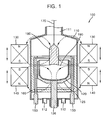
- FIG. 1 is a schematic sectional view of a silicon ingot growth apparatus used in a method for growing a silicon ingot according to an exemplary embodiment
- FIG. 2 is a flowchart illustrating the method for growing the silicon ingot according to the exemplary embodiment
- FIGS. 3A to 3C are schematic sectional views illustrating an operation for melting silicon in a quartz crucible in the method for growing the silicon ingot according to the exemplary embodiment
- FIG. 4 is a schematic sectional view illustrating effect of oxygen in a silicon melt on crystallization of the quartz crucible in the method for growing the silicon ingot according to the exemplary embodiment
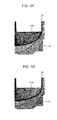
- FIG. 5A illustrates a simulation result of convection form when a magnetic field lower than 500 Gauss is applied
- FIG. 5B illustrates a simulation result of convection form when a magnetic field higher than 500 Gauss is applied, in the method for growing the silicon ingot according to the exemplary embodiment
- FIG. 6 illustrates a heat transfer process when a magnetic field is applied in the method for growing the silicon ingot according to the exemplary embodiment
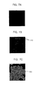
- FIGS. 7A to 7C are photographs illustrating amounts of flaking in a quartz crucible in the method for growing the silicon ingot according to the exemplary embodiment.
- FIG. 1 is a schematic sectional view of a silicon ingot growth apparatus used in a method for growing a silicon ingot according to an exemplary embodiment.
- the silicon ingot growth apparatus 100 includes a main body 110, a quartz crucible 120, a support 125, an upper electromagnet 130, a lower electromagnet 140, a heater 150, a heat-insulating wall 160 and a cable 170.
- the main body 110 includes a receiving portion formed therein, and an outlet 111 disposed in an upper portion of the main body 110 for pulling out a grown silicon ingot 180.
- the main body 110 further includes a gas inlet (not shown) for supplying an inert gas such as argon (Ar), neon (Ne) and nitrogen (N 2 ) to a silicon melt 190, and a gas outlet 112 for exhausting a gas therefrom.
- an inert gas such as argon (Ar), neon (Ne) and nitrogen (N 2 )
- the quartz crucible 120 with a receiving portion is placed in the main body 110.
- Poly-crystalline silicon is contained in the receiving portion of the quartz crucible 120.
- the quartz crucible 120 is heated by a heater 150, the poly-crystalline silicon is melted to a silicon melt in the quartz crucible 120.
- the support 125 is formed of graphite surrounding the quartz crucible 120 and fixed on a rotation axis 126.
- the rotation axis 126 is rotated and moved up and down by a driver (not shown), so that the quartz crucible 120 can be moved up while being rotated.
- the quartz crucible is moved up and down through the rotation axis 120 to keep an interface between the silicon ingot 180 and the silicon melt 190 at a predetermined height.
- the upper electromagnet 130 is disposed in an upper portion outside the main body 110, and the lower electromagnet 140 is disposed in a lower portion outside the main body 110. If the upper electromagnet 130 and the lower electromagnet are disposed as shown in FIG. 1 , and current or voltage is applied to them, a cusp magnetic field is formed in the quartz crucible 120 as indicated by the arrows.
- the heater 150 is formed in a cylindrical shape to surround a side surface of the support 125 with a predetermined gap therebetween.
- the heater 150 can heat the inside of the quartz crucible 120 to above approximately 1,500 °C to melt the poly-crystalline silicon inside the quartz crucible.
- the heat-insulating wall 160 surrounds the heater 150 and the support 125 completely.
- the heat-insulating wall 160 prevents heat emitted from the heater 150 from being diffused to an outer surface of the main body 110, thereby improving the thermal efficiency.
- the heat-insulating wall 160 shields an outer wall of the main body 110 from a high temperature radiation, keeps the temperature inside the main body 110, and maintains the state of the silicon melt 190.
- the cable 170 is extended to an upper portion of the main body 110 through the outlet 111 out which a silicon ingot 180 is pulled.
- a driver (not shown) for rotating and moving up and down the cable 170.
- a silicon seed crystal which is dipped into the silicon melt 190 to grow the silicon ingot 180.
- the driver (not shown) pulls up the cable 170 while rotating the cable 170, during the silicon ingot growth.
- the cable 170 is rotated in the opposite direction to the rotation of the support 120.
- FIG. 2 is a flowchart illustrating the method for growing the silicon ingot according to the exemplary embodiment.
- poly-crystalline silicon is charged in the quartz crucible 120.
- the poly-crystalline silicon includes a chuck poly or a granule poly.
- a dopant may also be charged in the quartz crucible 120 together with the poly-crystalline silicon.
- the dopant determines whether the grown silicon ingot becomes an n-type silicon ingot or a p-type silicon ingot.
- phosphorous (P) or antimony (Sb) may be used as the dopant.
- boron (B) may be used as the dopant.
- an internal pressure of the quartz crucible 120 is controlled between 50 Torr and 400 Torr, preferably between 50 Torr and 100 Torr.
- the internal pressure of the quartz crucible 120 may be controlled by supplying inert gases such as argon, neon, and nitrogen through the gas inlet (not shown).
- the quartz crucible 120 is heated by the heater 150 to melt the silicon in the quartz crucible 120.
- FIGS. 3A to 3C are schematic sectional views illustrating the operation S230 for melting the silicon in the quartz crucible in the method for growing the silicon ingot according to the exemplary embodiment.
- heat from the heater 150 is concentrated to a certain portion 310 of silicon in the quartz crucible 120 so that the portion 310 is primarily melted.
- a first collapse occurs, and the melted silicon fills the quartz crucible from the bottom as shown in FIG. 3B .
- FIG. 3C the unmelted silicon is collapsed and melted.
- the unmelted silicon is melted using the heat of the hot silicon melt around the unmelted silicon. That is, the unmelted silicon serves to lower the temperature of the silicon melt. Accordingly, unless sufficient heat is supplied from the heater 150, the unmelted silicon is not melted, rather still remains in the solid state.
- Table 1 lists the crystallization degree of the inner surface of the quartz crucible 120 according to the internal pressure of the quartz crucible 120.
- the crystallization degree of the inner surface of the quartz crucible 120 is represented by an area fraction of the unflaked area in an area of 5 cm x 5 cm in an inner bottom surface of the quartz crucible 120 after the overall process.
- the magnetic field was controlled to be lower than 300 Gauss throughout from the silicon melting to the silicon ingot growth.
- Example 2 15 ⁇ 50 50 ⁇ 100 74
- the fraction of unflaked area in the internal surface of the quartz crucible 120 was from 74 % to 88 %.
- the internal pressure of the quartz crucible 120 was controlled to be lower than 40 Torr (Example 1)
- the fraction of unflaked area in the internal surface of the quartz crucible 120 was only 26 %.
- the case where the internal pressure of the quartz crucible 120 was controlled between 100 Torr and 400 Torr showed similar results to that of the case where the internal pressure was controlled between 50 Torr and 100 Torr.
- the internal pressure of the quartz crucible 120 is preferably controlled from 50 Torr to 400 Torr, and more preferably, from 50 Torr to 100 Torr.
- the melting of the silicon is not a process for growing a single crystal, there is no possibility that poly-crystals are produced or defects are generated by oxides at a pressure from 50 Torr to 400 Torr, preferably from 50 Torr to 100 Torr. Consequently, it is preferable that the pressure is controlled higher during the melting of the silicon than during the growing of the single crystalline silicon, which will be described later.
- a magnetic field above 500 Gauss is applied in the quartz crucible 120.
- a cusp magnetic field is used, which is generated by applying current to the upper electromagnet 130 and lower electromagnet 140 as shown in FIG. 1 .
- FIG. 5A illustrates a simulation result of convection form when the magnetic field lower than 500 Gauss is applied
- FIG. 5B illustrates a simulation result of convection form when the magnetic field higher than 500 Gauss is applied, in the method for growing the silicon ingot according to the exemplary embodiment.
- the magnetic field of 500 Gauss or higher after 80 % or more of the silicon is melted, rather than to apply the magnetic field of 500 Gauss or higher from the initial stage of the silicon melting.
- 80 % or more of the silicon is melted, unmelted silicon floats on a surface of the silicon melt. Accordingly, even if the magnetic field of 500 Gauss or higher is applied, the melting time is not increased significantly.
- Table 2 lists the crystallization degree of the inner surface of the quartz crucible according to the magnitude of the magnetic field applied in the quartz crucible 120.
- the crystallization degree of the inner surface of the quartz crucible 120 is represented by an area fraction of the unflaked area in an area of 5 cm x 5 cm in an inner bottom surface of the quartz crucible 120 after the overall process, as described above.
- the pressure inside the quartz crucible was controlled between 10 Torr and 50 Torr.
- a magnetic field of 300 Gauss or lower was applied.
- a magnetic field of 500 Gauss or higher is applied from an initial stage of the silicon melting, the overall process time is increased as described above. Therefore, it is more preferable that, as listed in Example 6, a magnetic field lower than 500 Gauss is applied in an initial stage of the silicon melting and a magnetic field of 500 Gauss or higher is applied after 80 % of the silicon is melted.
- the effect of the magnetic field is not improved any more if it is higher than 500 Gauss, regardless of whether it is 500 Gauss or 1,000 Gauss. Therefore, the magnetic field may have any magnitude range allowable by the ingot growth apparatus 100. However, because, as the magnitude of the magnetic field is increased, the process cost is also increased, it is preferable to apply the lowest magnetic field that can prevent the flaking of the quartz crucible 120.
- the Experiments 5 to 7 in Table 2 were performed at the typical pressure from 10 Torr to 50 Torr. However, it is advantageous to the crystal growth to control the internal pressure between 50 Torr and 400 Torr, preferably between 50 Torr and 100 Torr. This is because, as such, it is possible to increase the oxygen concentration at the inner surface of the quartz crucible 120, and the temperature difference between the inner surface of the quartz crucible 120 and the center of the silicon melt.
- FIGS. 7A to 7C are photographs of the samples of Examples 6, 3 and 5 having a size of 5 cm x 5 cm, respectively.
- Example 6 no flaking was observed as shown in FIG. 7A .
- Example 3 the flaking was observed in a certain area 710, which corresponds to 12 % of the overall area, as shown in FIG. 7B .
- FIG. 7B the experimental condition of Example 5
- most of the area 720 was flaked out.
- the internal temperature of the quartz crucible 120 is kept constant to remove impurities and stabilize the silicon melt 190.
- a magnetic field lower than 500 Gauss is applied in the quartz crucible 120.
- the magnetic field is decreased to below 500 Gauss, preferably to below 300 Gauss.
- the pressure is maintained at 50 Torr to 400 Torr, preferably at 50 Torr to 100 Torr.
- the present invention is not limited thereto.
- the present invention may also be applied to the case where a magnetic field is applied in parallel or perpendicular to the bottom surface of the quartz crucible 120.
- the silicon ingot 180 is prepared by performing a dipping process for contacting the silicon seed crystal connected to the cable 170 with the silicon melt, a necking process for growing the single crystalline silicon ingot 180, a shouldering process, and a tailing process for separating the grown silicon ingot 180 from the silicon melt 190.
- the exemplary embodiments it is possible to easily accelerate the crystallization of the inner surface of the quartz crucible by appropriately controlling the internal pressure of the quartz crucible, and application time and magnitude of the magnetic field during the melting of the silicon and during the growing of the silicon ingot. Therefore, there is no need for additional process during the preparation of the quartz crucible. In addition, because the crystallization of the inner surface of the quartz crucible is accelerated, the flaking of the quartz crucible can be prevented. As a result, it is possible to improve the property and the yield of the silicon ingot.
Landscapes
- Chemical & Material Sciences (AREA)
- Engineering & Computer Science (AREA)
- Crystallography & Structural Chemistry (AREA)
- Materials Engineering (AREA)
- Metallurgy (AREA)
- Organic Chemistry (AREA)
- Crystals, And After-Treatments Of Crystals (AREA)
- Silicon Compounds (AREA)
Applications Claiming Priority (1)
| Application Number | Priority Date | Filing Date | Title |
|---|---|---|---|
| KR1020070099677A KR100942185B1 (ko) | 2007-10-04 | 2007-10-04 | 실리콘 잉곳 성장방법 |
Publications (2)
| Publication Number | Publication Date |
|---|---|
| EP2045372A2 true EP2045372A2 (de) | 2009-04-08 |
| EP2045372A3 EP2045372A3 (de) | 2010-08-18 |
Family
ID=40289138
Family Applications (1)
| Application Number | Title | Priority Date | Filing Date |
|---|---|---|---|
| EP08015636A Withdrawn EP2045372A3 (de) | 2007-10-04 | 2008-09-04 | Verfahren zum Züchten eines Siliziumstabes |
Country Status (5)
| Country | Link |
|---|---|
| US (1) | US20090090295A1 (de) |
| EP (1) | EP2045372A3 (de) |
| JP (1) | JP2009091233A (de) |
| KR (1) | KR100942185B1 (de) |
| CN (1) | CN101435107A (de) |
Families Citing this family (8)
| Publication number | Priority date | Publication date | Assignee | Title |
|---|---|---|---|---|
| KR101303422B1 (ko) * | 2011-03-28 | 2013-09-05 | 주식회사 엘지실트론 | 단결정 잉곳의 제조방법 및 이에 의해 제조된 단결정 잉곳과 웨이퍼 |
| CN102154687B (zh) * | 2011-05-04 | 2012-07-04 | 杭州慧翔电液技术开发有限公司 | 大直径单晶炉勾型电磁场装置 |
| WO2013031091A1 (ja) * | 2011-09-01 | 2013-03-07 | 信越半導体株式会社 | シリコン単結晶の製造方法 |
| JP5823947B2 (ja) * | 2012-12-27 | 2015-11-25 | トヨタ自動車株式会社 | SiC単結晶の製造方法 |
| JP6930435B2 (ja) | 2018-01-17 | 2021-09-01 | 株式会社Sumco | 原料供給方法およびシリコン単結晶の製造方法 |
| JP6844560B2 (ja) | 2018-02-28 | 2021-03-17 | 株式会社Sumco | シリコン融液の対流パターン制御方法、シリコン単結晶の製造方法、および、シリコン単結晶の引き上げ装置 |
| KR102492237B1 (ko) * | 2020-11-25 | 2023-01-26 | 에스케이실트론 주식회사 | 실리콘 단결정 잉곳의 성장 방법 및 장치 |
| CN114959880B (zh) * | 2022-05-27 | 2024-02-13 | 西安奕斯伟材料科技股份有限公司 | 一种用于生产单晶硅棒的石英坩埚、坩埚组件及拉晶炉 |
Citations (1)
| Publication number | Priority date | Publication date | Assignee | Title |
|---|---|---|---|---|
| KR20070099677A (ko) | 2005-01-31 | 2007-10-09 | 총칭 하이푸 테크놀로지 코 엘티디 | 배지를 포함한 체강 전달, 체강 인입 및 초음파 차단을 위한 장치 |
Family Cites Families (9)
| Publication number | Priority date | Publication date | Assignee | Title |
|---|---|---|---|---|
| US5268063A (en) * | 1990-04-27 | 1993-12-07 | Sumitomo Sitix Co., Ltd. | Method of manufacturing single-crystal silicon |
| JPH08143391A (ja) * | 1993-06-01 | 1996-06-04 | Texas Instr Inc <Ti> | チョクラルスキ結晶引上げ装置に使用する螺旋加熱器 |
| JP3228173B2 (ja) * | 1997-03-27 | 2001-11-12 | 住友金属工業株式会社 | 単結晶製造方法 |
| JPH10297994A (ja) * | 1997-04-25 | 1998-11-10 | Sumitomo Sitix Corp | シリコン単結晶育成方法 |
| JP3360626B2 (ja) * | 1998-12-01 | 2002-12-24 | 三菱住友シリコン株式会社 | シリコン単結晶の製造方法 |
| JP3598972B2 (ja) * | 2000-12-20 | 2004-12-08 | 三菱住友シリコン株式会社 | シリコン単結晶の製造方法 |
| JP2004315258A (ja) * | 2003-04-14 | 2004-11-11 | Shin Etsu Handotai Co Ltd | 単結晶の製造方法 |
| KR100840751B1 (ko) * | 2005-07-26 | 2008-06-24 | 주식회사 실트론 | 고품질 실리콘 단결정 잉곳 제조 방법, 성장 장치 및그로부터 제조된 잉곳 , 웨이퍼 |
| JP2007197300A (ja) * | 2005-12-27 | 2007-08-09 | Sumco Corp | シリコン単結晶引上方法 |
-
2007
- 2007-10-04 KR KR1020070099677A patent/KR100942185B1/ko active Active
-
2008
- 2008-09-04 EP EP08015636A patent/EP2045372A3/de not_active Withdrawn
- 2008-09-08 US US12/206,373 patent/US20090090295A1/en not_active Abandoned
- 2008-09-11 JP JP2008233692A patent/JP2009091233A/ja active Pending
- 2008-09-26 CN CNA2008102114938A patent/CN101435107A/zh active Pending
Patent Citations (1)
| Publication number | Priority date | Publication date | Assignee | Title |
|---|---|---|---|---|
| KR20070099677A (ko) | 2005-01-31 | 2007-10-09 | 총칭 하이푸 테크놀로지 코 엘티디 | 배지를 포함한 체강 전달, 체강 인입 및 초음파 차단을 위한 장치 |
Also Published As
| Publication number | Publication date |
|---|---|
| CN101435107A (zh) | 2009-05-20 |
| JP2009091233A (ja) | 2009-04-30 |
| KR20090034465A (ko) | 2009-04-08 |
| EP2045372A3 (de) | 2010-08-18 |
| US20090090295A1 (en) | 2009-04-09 |
| KR100942185B1 (ko) | 2010-02-11 |
Similar Documents
| Publication | Publication Date | Title |
|---|---|---|
| EP2045372A2 (de) | Verfahren zum Züchten eines Siliziumstabes | |
| EP2705178B1 (de) | Wachstum eines gleichmässig dotierten siliciumstabs durch alleinige dotierung nur der anfänglichen ladung | |
| US7226506B2 (en) | Single crystal silicon producing method, single crystal silicon wafer producing method, seed crystal for producing single crystal silicon, single crystal silicon ingot, and single crystal silicon wafer | |
| KR101997565B1 (ko) | 실리콘 단결정의 제조방법 | |
| JP4367213B2 (ja) | シリコン単結晶の製造方法 | |
| US7229495B2 (en) | Silicon wafer and method for producing silicon single crystal | |
| JP5671057B2 (ja) | マイクロピット密度(mpd)が低いゲルマニウムのインゴットを製造する方法、およびゲルマニウム結晶を成長させる装置 | |
| EP2143833A1 (de) | Siliziumkristallmaterial und verfahren zur herstellung eines fz-siliziumeinkristalls damit | |
| JP4060106B2 (ja) | 一方向凝固シリコンインゴット及びこの製造方法並びにシリコン板及び太陽電池用基板及びスパッタリング用ターゲット素材 | |
| EP1538242B1 (de) | Heizeinrichtung zum kristallziehen, vorrichtung zum kristallziehen und kristallziehverfahren | |
| KR100331552B1 (ko) | 잉곳-용융물 경계의 중앙 및 가장자리에서의 온도구배의 조절에 의한 단결정 실리콘 잉곳의 제조를 위한 초크랄스키 풀러, 상기 초크랄스키 풀러용 열차단체 및 상기 초크랄스키 풀러의 개량방법. | |
| KR20050120707A (ko) | 단결정의 제조방법 | |
| JPWO1999037833A1 (ja) | 単結晶引き上げ装置 | |
| CN1995486B (zh) | 生产单晶硅的方法 | |
| CN212451745U (zh) | 碳化硅单晶快速扩径生长系统 | |
| JPH0748200A (ja) | 単結晶の製造方法 | |
| JP2004175620A (ja) | 単結晶の製造方法 | |
| JP4341379B2 (ja) | 単結晶の製造方法 | |
| JP4899608B2 (ja) | 半導体単結晶の製造装置及び製造方法 | |
| JP3885245B2 (ja) | 単結晶引上方法 | |
| JP2004269335A (ja) | 単結晶の製造方法 | |
| KR100749938B1 (ko) | 고품질 실리콘 단결정 잉곳 성장장치 및 성장방법 | |
| JPH09255480A (ja) | 単結晶引き上げ装置及び単結晶引き上げ方法 | |
| KR100784585B1 (ko) | 비대칭 자기장을 이용한 반도체 단결정 제조 방법 및 그장치 | |
| JP2007210865A (ja) | シリコン単結晶引上装置 |
Legal Events
| Date | Code | Title | Description |
|---|---|---|---|
| PUAI | Public reference made under article 153(3) epc to a published international application that has entered the european phase |
Free format text: ORIGINAL CODE: 0009012 |
|
| AK | Designated contracting states |
Kind code of ref document: A2 Designated state(s): AT BE BG CH CY CZ DE DK EE ES FI FR GB GR HR HU IE IS IT LI LT LU LV MC MT NL NO PL PT RO SE SI SK TR |
|
| AX | Request for extension of the european patent |
Extension state: AL BA MK RS |
|
| PUAL | Search report despatched |
Free format text: ORIGINAL CODE: 0009013 |
|
| AK | Designated contracting states |
Kind code of ref document: A3 Designated state(s): AT BE BG CH CY CZ DE DK EE ES FI FR GB GR HR HU IE IS IT LI LT LU LV MC MT NL NO PL PT RO SE SI SK TR |
|
| AX | Request for extension of the european patent |
Extension state: AL BA MK RS |
|
| AKY | No designation fees paid | ||
| STAA | Information on the status of an ep patent application or granted ep patent |
Free format text: STATUS: THE APPLICATION IS DEEMED TO BE WITHDRAWN |
|
| 18D | Application deemed to be withdrawn |
Effective date: 20110219 |