EP2048699A2 - Antireflektionsbeschichtungen für Photovoltaik-Anwendungen - Google Patents
Antireflektionsbeschichtungen für Photovoltaik-Anwendungen Download PDFInfo
- Publication number
- EP2048699A2 EP2048699A2 EP08166488A EP08166488A EP2048699A2 EP 2048699 A2 EP2048699 A2 EP 2048699A2 EP 08166488 A EP08166488 A EP 08166488A EP 08166488 A EP08166488 A EP 08166488A EP 2048699 A2 EP2048699 A2 EP 2048699A2
- Authority
- EP
- European Patent Office
- Prior art keywords
- cyclic
- singly
- branched
- saturated
- linear
- Prior art date
- Legal status (The legal status is an assumption and is not a legal conclusion. Google has not performed a legal analysis and makes no representation as to the accuracy of the status listed.)
- Withdrawn
Links
Images


Classifications
-
- H—ELECTRICITY
- H10—SEMICONDUCTOR DEVICES; ELECTRIC SOLID-STATE DEVICES NOT OTHERWISE PROVIDED FOR
- H10F—INORGANIC SEMICONDUCTOR DEVICES SENSITIVE TO INFRARED RADIATION, LIGHT, ELECTROMAGNETIC RADIATION OF SHORTER WAVELENGTH OR CORPUSCULAR RADIATION
- H10F10/00—Individual photovoltaic cells, e.g. solar cells
-
- H—ELECTRICITY
- H10—SEMICONDUCTOR DEVICES; ELECTRIC SOLID-STATE DEVICES NOT OTHERWISE PROVIDED FOR
- H10F—INORGANIC SEMICONDUCTOR DEVICES SENSITIVE TO INFRARED RADIATION, LIGHT, ELECTROMAGNETIC RADIATION OF SHORTER WAVELENGTH OR CORPUSCULAR RADIATION
- H10F77/00—Constructional details of devices covered by this subclass
- H10F77/30—Coatings
- H10F77/306—Coatings for devices having potential barriers
- H10F77/311—Coatings for devices having potential barriers for photovoltaic cells
- H10F77/315—Coatings for devices having potential barriers for photovoltaic cells the coatings being antireflective or having enhancing optical properties
-
- C—CHEMISTRY; METALLURGY
- C23—COATING METALLIC MATERIAL; COATING MATERIAL WITH METALLIC MATERIAL; CHEMICAL SURFACE TREATMENT; DIFFUSION TREATMENT OF METALLIC MATERIAL; COATING BY VACUUM EVAPORATION, BY SPUTTERING, BY ION IMPLANTATION OR BY CHEMICAL VAPOUR DEPOSITION, IN GENERAL; INHIBITING CORROSION OF METALLIC MATERIAL OR INCRUSTATION IN GENERAL
- C23C—COATING METALLIC MATERIAL; COATING MATERIAL WITH METALLIC MATERIAL; SURFACE TREATMENT OF METALLIC MATERIAL BY DIFFUSION INTO THE SURFACE, BY CHEMICAL CONVERSION OR SUBSTITUTION; COATING BY VACUUM EVAPORATION, BY SPUTTERING, BY ION IMPLANTATION OR BY CHEMICAL VAPOUR DEPOSITION, IN GENERAL
- C23C16/00—Chemical coating by decomposition of gaseous compounds, without leaving reaction products of surface material in the coating, i.e. chemical vapour deposition [CVD] processes
- C23C16/22—Chemical coating by decomposition of gaseous compounds, without leaving reaction products of surface material in the coating, i.e. chemical vapour deposition [CVD] processes characterised by the deposition of inorganic material, other than metallic material
- C23C16/30—Deposition of compounds, mixtures or solid solutions, e.g. borides, carbides, nitrides
-
- H—ELECTRICITY
- H10—SEMICONDUCTOR DEVICES; ELECTRIC SOLID-STATE DEVICES NOT OTHERWISE PROVIDED FOR
- H10F—INORGANIC SEMICONDUCTOR DEVICES SENSITIVE TO INFRARED RADIATION, LIGHT, ELECTROMAGNETIC RADIATION OF SHORTER WAVELENGTH OR CORPUSCULAR RADIATION
- H10F71/00—Manufacture or treatment of devices covered by this subclass
-
- H—ELECTRICITY
- H10—SEMICONDUCTOR DEVICES; ELECTRIC SOLID-STATE DEVICES NOT OTHERWISE PROVIDED FOR
- H10F—INORGANIC SEMICONDUCTOR DEVICES SENSITIVE TO INFRARED RADIATION, LIGHT, ELECTROMAGNETIC RADIATION OF SHORTER WAVELENGTH OR CORPUSCULAR RADIATION
- H10F77/00—Constructional details of devices covered by this subclass
- H10F77/70—Surface textures, e.g. pyramid structures
-
- H—ELECTRICITY
- H10—SEMICONDUCTOR DEVICES; ELECTRIC SOLID-STATE DEVICES NOT OTHERWISE PROVIDED FOR
- H10F—INORGANIC SEMICONDUCTOR DEVICES SENSITIVE TO INFRARED RADIATION, LIGHT, ELECTROMAGNETIC RADIATION OF SHORTER WAVELENGTH OR CORPUSCULAR RADIATION
- H10F77/00—Constructional details of devices covered by this subclass
- H10F77/70—Surface textures, e.g. pyramid structures
- H10F77/703—Surface textures, e.g. pyramid structures of the semiconductor bodies, e.g. textured active layers
-
- H—ELECTRICITY
- H10—SEMICONDUCTOR DEVICES; ELECTRIC SOLID-STATE DEVICES NOT OTHERWISE PROVIDED FOR
- H10P—GENERIC PROCESSES OR APPARATUS FOR THE MANUFACTURE OR TREATMENT OF DEVICES COVERED BY CLASS H10
- H10P14/00—Formation of materials, e.g. in the shape of layers or pillars
- H10P14/60—Formation of materials, e.g. in the shape of layers or pillars of insulating materials
- H10P14/69—Inorganic materials
- H10P14/6903—Inorganic materials containing silicon
- H10P14/6905—Inorganic materials containing silicon being a silicon carbide or silicon carbonitride and not containing oxygen, e.g. SiC or SiC:H
-
- Y—GENERAL TAGGING OF NEW TECHNOLOGICAL DEVELOPMENTS; GENERAL TAGGING OF CROSS-SECTIONAL TECHNOLOGIES SPANNING OVER SEVERAL SECTIONS OF THE IPC; TECHNICAL SUBJECTS COVERED BY FORMER USPC CROSS-REFERENCE ART COLLECTIONS [XRACs] AND DIGESTS
- Y02—TECHNOLOGIES OR APPLICATIONS FOR MITIGATION OR ADAPTATION AGAINST CLIMATE CHANGE
- Y02E—REDUCTION OF GREENHOUSE GAS [GHG] EMISSIONS, RELATED TO ENERGY GENERATION, TRANSMISSION OR DISTRIBUTION
- Y02E10/00—Energy generation through renewable energy sources
- Y02E10/50—Photovoltaic [PV] energy
- Y02E10/547—Monocrystalline silicon PV cells
Definitions
- This invention relates to photovoltaic devices, particularly photovoltaic devices comprising thin layers of semiconductor materials, such as thin layers of monocrystalline or multicrystalline silicon. More particularly, this invention relates to photovoltaic devices comprising an antireflective layer comprising an amorphous silicon carbide material that are highly efficient in comparison to conventionally produced cells.
- Photovoltaic (“PV”) cells convert light energy into electrical energy.
- Most photovoltaic cells are fabricated from either monocrystalline silicon or multicrystalline silicon. Silicon is generally used because it is readily available at a reasonable cost due to its use in the microelectronics industry and because it has the proper balance of electrical, physical and chemical properties for use to fabricate photovoltaic cells.
- silicon is typically doped with a dopant of either positive or negative conductivity type, and is typically cut into thin substrates, usually in the form of wafers or ribbons, by various methods known in the art.
- the surface of the substrate such as a wafer, intended to face incident light is designated as the front surface and the surface opposite the front surface is referred to as the back surface.
- positive conductivity type is commonly designated as “p” and negative conductivity type is designated as “n.”
- p and n are used only to indicate opposing conductivity types.
- p and n mean positive and negative respectively but can also mean negative and positive respectively.
- the key to the operation of a photovoltaic cell is the creation of a p-n junction, usually formed by further doping the front surface of the silicon substrate to form a layer of opposite conductivity type from the doped silicon substrate. Such a layer is commonly referred to as the emitter layer. In the case of a p-doped substrate, the emitter layer would be formed by doping the front surface with an n-type dopant.
- the p-n junction is the interface between the p-doped region and the n-doped region.
- the p-n junction allows the migration of electron-hole pairs in response to incident photons which causes a potential difference across the front and back surfaces of a substrate wafer.
- Fabrication of a photovoltaic cell generally begins with a p-doped substrate.
- the substrate typically in the form of a wafer, is then exposed to an n-dopant to form an emitter layer and a p-n junction.
- the n-doped layer is formed by first depositing an n-dopant onto the surface of the substrate using techniques commonly employed in the art such as, for example, spray on, spin on, chemical vapor deposition, or other deposition methods.
- the n-dopant is driven into the surface of the silicon substrate to further diffuse the n-dopant into the substrate surface (the n-doped layer is commonly referred to as an "emitter” layer).
- This "drive-in” step is commonly accomplished by exposing the wafer to heat, often in combination with a gas stream comprising oxygen, nitrogen, steam, or a combination thereof. A p-n junction is thereby formed at the boundary region between the n-doped layer and the p-doped silicon substrate, which allows the charge carriers to migrate in response to incident light.
- Efficiency of a photovoltaic cell is determined by the capacity of the cell to convert incident light energy into electrical energy.
- Several modifications to the design and production of photovoltaic cells have been developed to increase conversion efficiency including the use of texturing, antireflective coatings, surface passivation, and back surface fields.
- Texturing of a photovoltaic cell reduces reflection of incident light by the photovoltaic cell surface. By reducing reflection, more incident light is available for conversion by the photovoltaic cell. Texturing is typically accomplished by chemical etching and in particular by anisotropic etching of the silicon substrate.
- Antireflective coatings are typically applied on textured surfaces to further reduce the reflection of incident light at the photovoltaic cell surface.
- the interface between the antireflective coating and the emitter layer of a photovoltaic device is critical in the overall performance of the device. For example, gaps or any other type of defect at this interface can adversely affect the efficient collection of charge.
- Prior art antireflective coatings such as, for example, oxides or silicon nitride are prone to formation of defects at this interface because of the high temperatures and plasma powers that are needed to deposit these materials. Accordingly, there is a need in the art for an antireflective coating that does not suffer from the above-mentioned drawbacks.
- the substrate is texturized.
- the antireflective coating may be formed by the chemical vapor deposition of a composition comprising an aminosilane, preferably bis(tertiarybutylamino)silane.
- the at least one precursor is at least one precursor selected from:
- the precursor may for example be: monomethylsilane, dimethylsilane, trimethylsilane, and tetramethylsilane. More preferably, the precursor is tetramethylsilane.
- composition used to form the antireflective coating further comprises a hydrocarbon.
- the hydrocarbon may be distinct from the at least one precursor.
- the hydrocarbon may, for example, be selected from:
- the hydrocarbon is selected from: cyclohexane, trimethylcyclohexane, 1-methyl-4(1-methylethyl)cyclohexane, cyclooctane, methylcyclooctane, cyclooctene, cyclooctadiene, cycloheptene, cyclopentene, 1,5,9-cyclododecatriene, ethylene, propylene, acetylene, neohexane, cyclohexene, vinylcyclohexane, dimethylcyclohexene, t-butylcyclohexene, alpha-terpinene, pinene, 1,5-dimethyl-1,5-cyclooctadiene, vinyl-cyclohexene, norbornane, spiro-nonane, decahydronaphthalene, camphene, norbornene, norbornadiene, and adamantan
- the at least one precursor is selected from:
- the precursor is more preferably selected from:
- amorphous silicon carbide antireflective coating represented by the formula Si v C x N u H y F z as defined above also includes amorphous silicon carbo-nitride when nitrogen is present in the film (i.e., when "u" is greater than 0).
- photovoltaic device means a solid-state electrical device that converts light directly into direct current electricity of voltage-current characteristics that are a function of the characteristics of the light source and the materials in and design of the device.
- photovoltaic device includes a photovoltaic cell but is not necessarily limited thereto.
- a photovoltaic device such as, for example, a photovoltaic cell according to the present invention is fabricated using a boron doped substrate comprising silicon, typically in the form of a wafer or a ribbon.
- the substrate can comprise monocrystalline silicon and the substrate can comprise multicrystalline silicon.
- silicon includes monocrystalline silicon and multicrystalline silicon unless expressly noted.
- One or more layers of additional material; for example, germanium, may be disposed over the substrate surface or incorporated into the substrate if desired.
- boron is widely used as the p-type dopant, other p-type dopants such as, for example, gallium or indium, can also be employed.
- Wafers are typically obtained by slicing silicon ingots, vapor phase deposition, liquid phase epitaxy or other known methods. Slicing can be via inner-diameter blade, continuous wire or other known sawing methods.
- the substrate can be cut into any generally flat shape, wafers are typically circular in shape. Generally, such wafers are typically less than 400 micrometers thick.
- substrates of the present invention are less than 200 micrometers thick, more preferably less than 150 micrometers thick, still more preferably less than 100 micrometers thick, and most preferably less than 50 micrometers thick.
- the substrates are at least 10 micrometers and, more preferably about 20 micrometers thick.
- Substrates employed in the present invention are typically cut from a cylindrical silicon block having a diameter in the range of from 100 mm to 200 mm.
- the substrate is preferably cleaned to remove any surface debris and cutting damage.
- this includes placing the substrate in a wet chemical bath such as, for example, a solution comprising any one of a base and peroxide mixture, an acid and peroxide mixture, a NaOH solution, or several other solutions known and used in the art.
- a wet chemical bath such as, for example, a solution comprising any one of a base and peroxide mixture, an acid and peroxide mixture, a NaOH solution, or several other solutions known and used in the art.
- the temperature and time required for cleaning depends on the specific solution employed. For example, a 25 wt % to 35 wt % aqueous NaOH solution can be used at a temperature in the range of 75 to 95°C for 20 to 70 seconds.
- the substrate is texturized by, for example, anisotropic etching of the crystallographic planes. Texturing is commonly in the form of pyramid-shapes depressed or projected from the substrate surface. The height or depth of the pyramid-shapes is typically from 4 to 7 micrometers.
- a low concentration aqueous NaOH solution at elevated temperature is typically employed to anisotropically etch the 100 plane revealing a 111 orientation plane in pyramid-shape projections.
- a "low concentration” solution means, preferably, a concentration of solute less than 7 wt %.
- Elelevated temperature as used herein means, preferably, a temperature greater than 80°C. Under such conditions, for example, a substrate would be placed in the solution for 10 to 30 minutes.
- An emitter layer is formed typically by doping the substrate with an n-type dopant.
- N-doping can be accomplished by depositing the n-dopant onto the substrate and then heating the substrate to "drive" the n-dopant into the substrate.
- Gaseous diffusion can be used to deposit the n-dopant onto the substrate surface.
- Other methods can also be used, however, such as, for example, ion implantation, solid state diffusion, or other methods used in the art to create an n-doped layer and a shallow p-n junction proximal to the substrate surface.
- Phosphorus is a preferred n-dopant, but any suitable n-dopant can be used alone or in combination such as, for example, arsenic, antimony or lithium.
- a plurality of substrates are placed in a tray such that the front and back surfaces and the edges of the substrate are exposed to the n-dopant.
- an emitter layer and p-n junction created in the n-doping process are formed along all of the surfaces of the substrate.
- the depth of the n-doped layer at the front surface is typically greater than 0.1 micrometer, preferably greater than 0.2 micrometers and is typically less than 0.5 micrometers, and preferably less than 0.3 micrometers.
- the surface dopant concentration of the emitter layer at the front surface is preferably greater than 10 18 atoms/cm 3 , more preferably greater than 10 19 atoms/cm 3 .
- the surface dopant concentration of the emitter layer at the front surface can be as high as saturation, but is typically less than 10 22 atoms/cm 3 , more preferably less than 10 21 atoms/cm 3 , most preferably the surface dopant concentration of the emitter layer is about 10 20 atoms/cm 3 .
- the n-doping process typically creates a layer of silicon oxide on the surfaces of the wafer, which is typically removed prior to application of an antireflective coating in favor of a coating.
- the silicon oxide can be removed through, for example, chemical etching in a wet chemical bath, typically a low concentration HF solution at ambient temperature for 10 to 40 seconds.
- the method of the present invention includes the step of forming an amorphous silicon carbide antireflective coating over at least one surface of the silicon substrate by chemical vapor deposition of a composition comprising a precursor selected from an organosilane, an aminosilane, and mixtures thereof.
- a composition comprising a precursor selected from an organosilane, an aminosilane, and mixtures thereof.
- the phrase "forming an amorphous silicon carbide antireflective coating over at least one surface of the silicon substrate is not restricted to the amorphous silicon carbide layer being directly over and in contact with the at least one surface of the silicon substrate it is disposed over.
- Other intervening materials or layers may be present. Examples of such other intervening materials or layers include materials and layers typically found in a photovoltaic cell such as, for example, a transparent conductor layer and a grid conductor layer.
- the antireflective coating according to the present invention is preferably formed by the chemical vapor deposition of a composition comprising (1) at least one precursor selected from an organosilane, an aminosilane, and mixtures thereof; and optionally (2) a hydrocarbon; preferably wherein the hydrocarbon is not removed from the antireflective coating after deposition.
- the at least one precursor selected from an organosilane, an aminosilane, and mixtures thereof which is suitable for use according to embodiments of the present invention that are suitable to form an amorphous silicon carbide antireflective layer either with or without a distinct hydrocarbon.
- the term "independently” should be understood to denote that the subject R group is not only independently selected relative to other R groups bearing different superscripts, but is also independently selected relative to any additional species of the same R group.
- R 1 n R 2 4-n Si when n is 2 or 3, the two or three R 1 groups need not be identical to each other or to R 2 .
- organosilanes include monomethylsilane, dimethylsilane, trimethylsilane, and tetramethylsilane.
- a preferred aminosilane is bis(tertiarybutylamino)silane.
- the above precursors may be mixed with light absorber or have attached light absorbing substituents, and may be mixed with other molecules of these classes and/or with molecules of the same classes. In other embodiments, the above precursors are employed as the sole components of the composition, i.e., without additional light absorbing molecules.
- hydrocarbons are optional components of the composition comprising the at least one precursor.
- the hydrocarbon functions to provide a species that absorbs light. Whether a species absorbs light at wavelengths less than 400 nm is measured by the ability of the resultant film to minimize light from being reflected such as, for example, back out of the photovoltaic device, yet be essentially transparent at higher wavelengths where the device absorbs light creating hole-electron pairs. Light absorption can be measured by any of a number of tools known in the art such as, for example, spectrophotometers, reflectometers and ellipsometers. Light absorption may also be interpreted as the imaginary portion of the refractive index.
- the hydrocarbon is an organic hydrocarbon and is distinct from the organosilane and the aminosilane. In preferred embodiments of the present invention, the organic hydrocarbon consists of only carbon and hydrogen atoms.
- hydrocarbons that are suitable for use in embodiments of the present invention wherein the hydrocarbon is distinct from the at least one precursor selected from an organosilane.
- the following compounds are suitable for use as light absorbers according to the invention:
- the at least one precursor and the light absorbing precursor are not necessarily different molecules and, in certain embodiments, the light absorber is a part of (e.g., covalently bound to) the structure-forming precursor. Precursors containing light absorbers bound to them are sometimes referred to herein as "light absorbing precursors.” Having the light absorber attached to the silicon-containing at least one precursor may be advantageous in achieving a higher efficiency of incorporation of light absorber into the film during the deposition process.
- two light absorbers attached to one Si in the precursor such as in diphenyl-diethylsilane, or two Si atoms attached to one light absorber, such as in 1,4-bis(diethylsilyl)cylcohex-2,5-diene, because a likely bond to break in a plasma during the deposition process is the Si-carbon bond.
- reaction of one Si-C (i.e., Si-hydrocarbon) bond in the plasma will result in incorporation of the light absorbing character in the deposited film.
- the following are non-limiting examples of such Si-based precursors having light absorbing capability.
- the light absorbing function is attributed to one or more of R 1 , R 2 , R 3 , R 4 , or R 7 :
- R 1 , R 3 and R 7 have a C 3 or larger hydrocarbon to act as light absorber, and an optional post-treatment process may be used to modify at least a portion of the light absorber.
- each of R 1 , R 2 , R 3 , R 4 , and R 7 in the formulas above are either hydrogen or a C 5 to C 7 hydrocarbon group.
- the above precursors may be mixed with other molecules of these same classes and/or with molecules of the same classes except where n and/or m are from 0 to 3.
- the hydrocarbon i.e., the light-absorbing component
- the hydrocarbon preferably is substantially not removed from the antireflective coating.
- the phrase "substantially not removed from the antireflective coating” refers to a feature of the present invention wherein carbon species from the hydrocarbon is desired to be present to participate in imparting antireflective character to the coating. Accordingly, although some carbon may be incidentally removed as a result of certain processing conditions after the amorphous silicon carbide antireflective layer has been deposited, the carbon is substantially present in the coating to absorb light at the required wavelengths.
- the amorphous silicon carbide antireflective layer is a thin film having not only light absorbing characteristics, but also improved surface passivation properties relative to for example silicon nitride deposited form PECVD based SiH 4 and NH 3 .
- the antireflective coatings of the present invention are compatible with the various chemical processes used to produce photovoltaic devices, and are capable of adhering to a variety of materials, such as silicon, SiO 2 , Si 3 N 4 , OSG, FSG, silicon carbide, hydrogenated silicon carbide, silicon nitride, hydrogenated silicon nitride, silicon carbonitride, hydrogenated silicon carbonitride, boronitride, low dielectric constant materials, photoresists, organic polymers, porous organic and inorganic materials, metals such as copper and aluminum, and diffusion barrier layers such as but not limited to TiN, Ti(C)N TaN, Ta(C)N, Ta, W, WN or W(C)N.
- materials such as silicon, SiO 2 , Si 3 N 4 , OSG, FSG, silicon carbide, hydrogenated silicon carbide, silicon nitride, hydrogenated silicon nitride, silicon carbonitride, hydrogenated silicon carbonitride, boronitride, low dielectric constant materials
- Such films are capable of adhering to at least one of the foregoing materials sufficiently to pass a conventional pull test, such as ASTM D3359-95a tape pull test, wherein a sample is considered to have passed the test if there is no discernible removal of film.
- the amorphous silicon carbide antireflective coating of the present invention is deposited to a thickness of from 0.002 to 10 microns, although the thickness can be varied as required and multiple layers can be applied.
- the blanket film deposited on a non-patterned surface has excellent uniformity, with a variation in thickness of less than 2% over 1 standard deviation across the substrate with a reasonable edge exclusion, wherein e.g., a 5mm outermost edge of the substrate is not included in the statistical calculation of uniformity.
- the amorphous silicon carbide antireflective coatings according to the present invention have a refractive index between 1.0 and 4.0 and, more preferably, between 1.7 and 2.3. Improved reflectivity over a range of wavelengths can be achieved with two or more films. For example, the more layers of the antireflective coating according to the present invention, the greater the range of wavelengths over which the reflectivity can be minimized. Typically with multiple layers, each layer will have a different refractive index.
- the absorptivity of the film also can be increased by altering the chemistry and deposition conditions for the film, as well as with optional posttreatments in order to tailor the film properties for the particular application.
- Antireflective coatings of the present invention do not require the use of an oxidant during deposition of the film.
- the absence of added oxidant to the gas phase which is defined for present purposes as a moiety that could oxidize organic groups (e.g., O 2 , N 2 O, ozone, hydrogen peroxide, NO, NO 2 , N 2 O 4 , or mixtures thereof), may facilitate the retention of the desired light absorbing species in the film. This allows the incorporation of the desired amount of carbon necessary to provide desired properties, such as light absorptivity and surface passivation.
- the precursors can be carried into the reactor separately from distinct sources or as a mixture.
- the precursors can be delivered to the reactor system by any number of means, preferably using a pressurized stainless steel vessel fitted with the proper valves and fittings to allow the delivery of liquid to the process reactor.
- mixtures of different precursors such as, for example, organosilanes and/or aminosilanes
- mixtures of different precursors such as, for example, organosilanes and/or aminosilanes
- combinations of multiple different light absorbers, and organosilanes and/or aminosilanes in combination with, for example, organosilane and/or aminosilanes species with attached light absorbers.
- Such embodiments facilitate adjusting the ratio of light absorber to Si in the final product, and /or enhance one or more critical properties of the structure.
- additional materials can be charged into the vacuum chamber prior to, during and/or after the deposition reaction.
- Such materials include, e.g., inert gas (e.g., He, Ar, N 2 , Kr, Xe, which may be employed as a carrier gas for lesser volatile precursors and/or which can promote the curing of the as-deposited materials and provide a more stable final film) and reactive substances, such as gaseous or liquid organic substances, NH 3 , and H 2 , are the preferred carrier gas.
- Energy is applied to the gaseous reagents to induce the gases to react and to form the film on the substrate.
- energy can be provided by (depending on the method employed), e.g., thermal, plasma, pulsed plasma, helicon plasma, high density plasma, inductively coupled plasma, and remote plasma methods.
- a secondary rf frequency source can be used to modify the plasma characteristics at the substrate surface.
- the coating is formed by plasma enhanced chemical vapor deposition. It is particularly preferred to generate a capacitively coupled plasma at a frequency of 13.56 MHz.
- Plasma power is preferably from 0.02 to 7 watts/cm 2 , more preferably 0.3 to 3 watts/cm 2 , based upon a surface area of the substrate.
- a carrier gas which possesses a low ionization energy to lower the electron temperature in the plasma which in turn will cause less fragmentation in the silicon based precursor and light absorber.
- this type of low ionization gas include NH 3 , CH 4 , Ar, Xe, Kr.
- the flow rate for each of the gaseous reagents preferably ranges from 10 to 5000 sccm, more preferably from 30 to 1000 sccm, per single 200 mm wafer.
- the individual rates are selected so as to provide the desired amounts of structure-former and light absorber in the film.
- the actual flow rates needed may depend upon wafer size and chamber configuration, and are in no way limited to 200 mm wafers or single wafer chambers.
- antireflective coating of the present invention has been demonstrated in connection with depositing a passivating antireflective coating, one of ordinary skill in the art will understand that the antireflective coatings of the present invention can be employed in connection with passivation of other substrates such as, for example, silicon, aluminum, metals, metal oxides, and barrier materials.
- the substrate is subjected to back surface etching to remove the p-n junction.
- the amorphous silicon carbide antireflective coating acts as a mask for the surfaces over which the antireflective coating is applied and, therefore, limits the etching to the uncoated portion of the substrate.
- Back surface etching is generally accomplished by placing the substrate in a chemical bath to remove the n-doped region from the back surface. The type of chemical used, the temperature of the bath and the time the substrate is kept in the bath are dependant upon the material used for the substrate.
- a 30 wt % aqueous NaOH bath at a temperature in the range of from 80°C to 92°C can be used for either monocrystalline or multicrystalline silicon.
- a monocrystalline silicon substrate would be exposed, for example, to the bath for 80 seconds to 100 seconds.
- a multicrystalline silicon substrate would generally be exposed to the bath for a longer period of time, for example, at least 3 minutes and up to, for example, 6 minutes.
- Any etch, and preferably a chemical etch, capable of removing the n-doped region of the back surface can be used at a temperature and for a time period that effects removal of the n-doped region of the back surface without substantial degradation of the antireflective coating.
- without substantial degradation is meant that the antireflective coating according to the present invention remains disposed over the front face, preferably also the edges, and, preferably, the back periphery of the substrate.
- the substrate can be cleaned with another chemical etch for example, a 4 wt % solution of HF prior to rinsing and drying the wafer.
- Back surface etching results in an untextured or substantially smooth back surface.
- substantially smooth back surface preferably means that the back surface is untextured except for the portion of the back surface, if any, over which a surface coating is disposed.
- Untextured as used herein, preferably means the absence of peaks or valleys on the substrate surface; for example, the absence of anisotropic etch surface topography or, as further example, having a surface topography consistent with isotropic etching.
- Back surface etching also results in a back surface which is free or substantially free of n-dopant and free or substantially free of a p-n junction.
- substantially free of n-dopant preferably means that the n-dopant has been etched from the back surface except that n-dopant may still be present at the portion of the back surface over which a surface coating is disposed.
- some n-dopant can be present in the unmasked region of the back surface at a substantially reduced surface concentration; for example, a surface concentration less than 10 15 atoms/cm 3 , preferably less than 10 13 atoms/cm 3 , more preferably less than 10 11 atoms/cm 3 .
- substantially free of a p-n junction proximal to the back surface means that the p-n junction proximal to the portion of the back surface over which the surface coating is not disposed is removed or rendered ineffective due to a decreased concentration of n-dopant, for example, a back surface concentration of n-dopant less than 10 15 atoms/cm 3 , preferably less than 10 13 atoms/cm 3 , more preferably less than 10 11 atoms/cm 3 , where the "atoms" are the atoms of dopant.
- Front and back contacts are then applied to the substrate.
- contacts are in the form of a conductive metal placed on or into the front and back surfaces.
- the contacts can be created using photolithographic methods, by laser grooving and electroless plating methods, screen printing, or any other method that provides good ohmic contact with the front and back surfaces respectively such that electric current can be drawn from the photovoltaic cell.
- the contacts are present in a design or pattern, for example a grid, fingers, lines, etc., and do not cover the entire front or back surface.
- the contacts are preferably screen printed onto the substrate using a conductive metal paste; for example, a silver paste.
- the contacts are typically screen printed onto one surface, allowed to dry and then printed on the opposite surface.
- the substrate is fired, typically at a temperature of from 800 to 950°C, to anneal the contacts to the substrate.
- FIG. 1 shows a cross-section of a photovoltaic cell 10 in accordance with one embodiment of the present invention.
- the photovoltaic cell 10 comprises a textured, boron-doped substrate 20. The texture is symbolically depicted as 26.
- a textured, n-doped layer 30, formed by phosphorus diffusion, is present.
- a p-n junction 32 is present where the boron doped substrate 20 meets the n-doped layer 30.
- Antireflective coating 40 according to the present invention is disposed over the n-doped layer 30 of the cell. Antireflective coating may also extend to the edges, the front surface, and the periphery of the back surface 24 of the cell.
- Films were deposited on silicon wafers by PECVD techniques employing organo-silanes such as, for example, trimethylsilane and tetramethyl silane (separately).
- the wafers were processed in a 200 mm Applied Materials DxZ PECVD chamber having a susceptor temperature in the range of from about 100°C to about 400°C.
- a pressure of approximately 3 torr (400 Pa) was used with flow rates between 50 sccm-1000 sccm.
- RF power 13.56 MHz
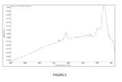
- Figure 2 is an IR spectra of the amorphous silicon carbide film showing the Si-C covalent bond at about 1200 cm -1 .
- Films were deposited on silicon wafers by PECVD techniques using bis t-butylamino silane (BTBAS) with or without ammonia(NH 3 ), The wafers were processed in a 200 mm Applied Materials DxZ PECVD chamber having a susceptor temperature range of from about 100°C to about 400°C. A pressure of approximately 2.0-4.0 torr (270-530 Pa) was used with flow rates of between 50 sccm-1 000 sccm. RF power (13.56 MHz) was varied between 200W-800W for 30-500 seconds, which produced a refractive index between 1.5-2.0.
- Figure 3 is an IR spectra of the amorphous silicon carbo-nitride film showing the Si-C covalent bond at about 1200 cm -1 and the presence of nitrogen at 3300 cm -1 .
Landscapes
- Chemical & Material Sciences (AREA)
- Engineering & Computer Science (AREA)
- Organic Chemistry (AREA)
- Chemical Kinetics & Catalysis (AREA)
- General Chemical & Material Sciences (AREA)
- Materials Engineering (AREA)
- Mechanical Engineering (AREA)
- Metallurgy (AREA)
- Inorganic Chemistry (AREA)
- Chemical Vapour Deposition (AREA)
- Photovoltaic Devices (AREA)
- Life Sciences & Earth Sciences (AREA)
- Sustainable Development (AREA)
- Manufacturing & Machinery (AREA)
- Surface Treatment Of Optical Elements (AREA)
- Formation Of Insulating Films (AREA)
Applications Claiming Priority (2)
| Application Number | Priority Date | Filing Date | Title |
|---|---|---|---|
| US97958507P | 2007-10-12 | 2007-10-12 | |
| US12/244,455 US8987039B2 (en) | 2007-10-12 | 2008-10-02 | Antireflective coatings for photovoltaic applications |
Publications (2)
| Publication Number | Publication Date |
|---|---|
| EP2048699A2 true EP2048699A2 (de) | 2009-04-15 |
| EP2048699A3 EP2048699A3 (de) | 2010-11-03 |
Family
ID=40263522
Family Applications (1)
| Application Number | Title | Priority Date | Filing Date |
|---|---|---|---|
| EP08166488A Withdrawn EP2048699A3 (de) | 2007-10-12 | 2008-10-13 | Antireflektionsbeschichtungen für Photovoltaik-Anwendungen |
Country Status (5)
| Country | Link |
|---|---|
| US (1) | US8987039B2 (de) |
| EP (1) | EP2048699A3 (de) |
| JP (2) | JP5390161B2 (de) |
| KR (1) | KR100986847B1 (de) |
| TW (1) | TWI440197B (de) |
Cited By (4)
| Publication number | Priority date | Publication date | Assignee | Title |
|---|---|---|---|---|
| WO2011056201A3 (en) * | 2009-10-27 | 2011-08-11 | Calisolar, Inc. | Polarization resistant solar cell |
| EP2478571A4 (de) * | 2009-09-18 | 2014-03-19 | Air Liquide | Solarzelle mit verbesserter leistung |
| EP3420117A4 (de) * | 2016-02-26 | 2020-01-15 | Versum Materials US, LLC | Zusammensetzungen und verfahren mit verwendung davon zur abscheidung von siliciumhaltigem film |
| JP2020515573A (ja) * | 2017-03-29 | 2020-05-28 | ディーエヌエフ カンパニー リミテッドDNF Co. Ltd. | シリルアミン化合物、それを含むシリコン含有薄膜蒸着用組成物、およびそれを用いたシリコン含有薄膜の製造方法 |
Families Citing this family (24)
| Publication number | Priority date | Publication date | Assignee | Title |
|---|---|---|---|---|
| CN102171384B (zh) * | 2008-05-28 | 2013-12-25 | 乔治洛德方法研究和开发液化空气有限公司 | 碳化硅基抗反射涂层 |
| US20100186811A1 (en) * | 2008-08-26 | 2010-07-29 | Sixtron Advanced Materials, Inc. | Silicon Carbonitride Antireflective Coating |
| CA2645474A1 (en) * | 2008-08-26 | 2010-02-26 | Sixtron Advanced Materials, Inc. | Silicon carbonitride antireflective coating |
| US8889235B2 (en) * | 2009-05-13 | 2014-11-18 | Air Products And Chemicals, Inc. | Dielectric barrier deposition using nitrogen containing precursor |
| FR2949775B1 (fr) * | 2009-09-10 | 2013-08-09 | Saint Gobain Performance Plast | Substrat de protection pour dispositif collecteur ou emetteur de rayonnement |
| FR2949776B1 (fr) | 2009-09-10 | 2013-05-17 | Saint Gobain Performance Plast | Element en couches pour l'encapsulation d'un element sensible |
| US9564542B2 (en) * | 2009-09-17 | 2017-02-07 | Tetrasun, Inc. | Selective transformation in functional films, and solar cell applications thereof |
| KR20110088172A (ko) * | 2010-01-28 | 2011-08-03 | 삼성전자주식회사 | 태양 전지 모듈 및 그 제조 방법 |
| WO2012002440A1 (ja) * | 2010-06-29 | 2012-01-05 | 京セラ株式会社 | 半導体基板の表面処理方法、半導体基板、および太陽電池の製造方法 |
| US8852848B2 (en) * | 2010-07-28 | 2014-10-07 | Z Electronic Materials USA Corp. | Composition for coating over a photoresist pattern |
| WO2012024676A2 (en) * | 2010-08-20 | 2012-02-23 | First Solar, Inc. | Anti-reflective photovoltaic module |
| JP5490031B2 (ja) * | 2011-02-04 | 2014-05-14 | 三菱電機株式会社 | 光起電力装置および光起電力モジュール |
| FR2973939A1 (fr) | 2011-04-08 | 2012-10-12 | Saint Gobain | Element en couches pour l’encapsulation d’un element sensible |
| US20130247967A1 (en) * | 2012-03-23 | 2013-09-26 | Scott Harrington | Gaseous ozone (o3) treatment for solar cell fabrication |
| WO2014037790A1 (en) * | 2012-09-05 | 2014-03-13 | Zinniatek Limited | Photovoltaic devices with three dimensional surface features and methods of making the same |
| US9401450B2 (en) * | 2013-12-09 | 2016-07-26 | Sunpower Corporation | Solar cell emitter region fabrication using ion implantation |
| KR101867855B1 (ko) * | 2014-03-17 | 2018-06-15 | 엘지전자 주식회사 | 태양 전지 |
| US9837259B2 (en) | 2014-08-29 | 2017-12-05 | Sunpower Corporation | Sequential etching treatment for solar cell fabrication |
| US12518963B2 (en) | 2017-03-29 | 2026-01-06 | Dnf Co., Ltd. | Composition for depositing silicon-containing thin film and method for manufacturing silicon-containing thin film using the same |
| KR20180110612A (ko) | 2017-03-29 | 2018-10-10 | (주)디엔에프 | 비스(아미노실릴)알킬아민 화합물을 포함하는 실리콘 함유 박막증착용 조성물 및 이를 이용하는 실리콘 함유 박막의 제조방법 |
| US11105960B2 (en) | 2017-12-19 | 2021-08-31 | Canon Kabushiki Kaisha | Optical element and method of producing the element, and optical instrument |
| JP2021013044A (ja) * | 2020-11-06 | 2021-02-04 | シャープ株式会社 | 光電変換素子 |
| CN118043288A (zh) * | 2021-10-07 | 2024-05-14 | 康宁股份有限公司 | 作为光学和保护性涂层的具有可调离子渗透性的氧化物涂层及其制造方法 |
| CN114203840A (zh) * | 2021-11-15 | 2022-03-18 | 一道新能源科技(衢州)有限公司 | 一种改善硼掺杂对绒面金字塔损伤的方法及装置 |
Family Cites Families (51)
| Publication number | Priority date | Publication date | Assignee | Title |
|---|---|---|---|---|
| JPS5895873A (ja) | 1981-12-02 | 1983-06-07 | Konishiroku Photo Ind Co Ltd | アモルフアスシリコン太陽電池 |
| JPS6067901A (ja) | 1983-09-24 | 1985-04-18 | Agency Of Ind Science & Technol | 水素化及び弗素化した非晶質炭化ケイ素薄膜を用いた光学素子 |
| US5472827A (en) | 1991-12-30 | 1995-12-05 | Sony Corporation | Method of forming a resist pattern using an anti-reflective layer |
| JP2897569B2 (ja) | 1991-12-30 | 1999-05-31 | ソニー株式会社 | レジストパターン形成時に用いる反射防止膜の条件決定方法と、レジストパターン形成方法 |
| US6541695B1 (en) | 1992-09-21 | 2003-04-01 | Thomas Mowles | High efficiency solar photovoltaic cells produced with inexpensive materials by processes suitable for large volume production |
| KR0134942B1 (ko) | 1993-06-11 | 1998-06-15 | 이다가끼 유끼오 | 비정질 경질 탄소막 및 그 제조 방법 |
| TW362118B (en) | 1995-10-30 | 1999-06-21 | Dow Corning | Method for depositing amorphous SiNC coatings |
| JPH10190031A (ja) | 1996-12-20 | 1998-07-21 | Tdk Corp | 太陽電池およびその製造方法 |
| US6020458A (en) | 1997-10-24 | 2000-02-01 | Quester Technology, Inc. | Precursors for making low dielectric constant materials with improved thermal stability |
| US6303523B2 (en) | 1998-02-11 | 2001-10-16 | Applied Materials, Inc. | Plasma processes for depositing low dielectric constant films |
| US6054379A (en) | 1998-02-11 | 2000-04-25 | Applied Materials, Inc. | Method of depositing a low k dielectric with organo silane |
| US6159871A (en) | 1998-05-29 | 2000-12-12 | Dow Corning Corporation | Method for producing hydrogenated silicon oxycarbide films having low dielectric constant |
| US6054206A (en) | 1998-06-22 | 2000-04-25 | Novellus Systems, Inc. | Chemical vapor deposition of low density silicon dioxide films |
| US6316167B1 (en) | 2000-01-10 | 2001-11-13 | International Business Machines Corporation | Tunabale vapor deposited materials as antireflective coatings, hardmasks and as combined antireflective coating/hardmasks and methods of fabrication thereof and application thereof |
| US6635583B2 (en) | 1998-10-01 | 2003-10-21 | Applied Materials, Inc. | Silicon carbide deposition for use as a low-dielectric constant anti-reflective coating |
| US6974766B1 (en) | 1998-10-01 | 2005-12-13 | Applied Materials, Inc. | In situ deposition of a low κ dielectric layer, barrier layer, etch stop, and anti-reflective coating for damascene application |
| US6171945B1 (en) | 1998-10-22 | 2001-01-09 | Applied Materials, Inc. | CVD nanoporous silica low dielectric constant films |
| BR0008585A (pt) | 1999-01-06 | 2001-11-06 | Union Carbide Chem Plastic | Composições de limpeza aquosas e seu uso |
| US6828289B2 (en) | 1999-01-27 | 2004-12-07 | Air Products And Chemicals, Inc. | Low surface tension, low viscosity, aqueous, acidic compositions containing fluoride and organic, polar solvents for removal of photoresist and organic and inorganic etch residues at room temperature |
| KR100307629B1 (ko) | 1999-04-30 | 2001-09-26 | 윤종용 | 하이드로 카본계의 가스를 이용한 반사방지막의 형성 및 적용방법 |
| US6312793B1 (en) | 1999-05-26 | 2001-11-06 | International Business Machines Corporation | Multiphase low dielectric constant material |
| US6875687B1 (en) | 1999-10-18 | 2005-04-05 | Applied Materials, Inc. | Capping layer for extreme low dielectric constant films |
| US6936405B2 (en) | 2000-02-22 | 2005-08-30 | Brewer Science Inc. | Organic polymeric antireflective coatings deposited by chemical vapor deposition |
| EP1127929B1 (de) | 2000-02-28 | 2009-04-15 | JSR Corporation | Zusammensetzung zur Filmerzeugung, Verfahren zur Filmerzeugung und Filme auf Basis von Siliciumoxid |
| US6441491B1 (en) | 2000-10-25 | 2002-08-27 | International Business Machines Corporation | Ultralow dielectric constant material as an intralevel or interlevel dielectric in a semiconductor device and electronic device containing the same |
| US6583048B2 (en) | 2001-01-17 | 2003-06-24 | Air Products And Chemicals, Inc. | Organosilicon precursors for interlayer dielectric films with low dielectric constants |
| US20030022800A1 (en) | 2001-06-14 | 2003-01-30 | Peters Darryl W. | Aqueous buffered fluoride-containing etch residue removers and cleaners |
| DE10131680A1 (de) | 2001-06-29 | 2003-01-23 | Voith Paper Patent Gmbh | Auftragsvorrichtung |
| US6627546B2 (en) | 2001-06-29 | 2003-09-30 | Ashland Inc. | Process for removing contaminant from a surface and composition useful therefor |
| US6943142B2 (en) | 2002-01-09 | 2005-09-13 | Air Products And Chemicals, Inc. | Aqueous stripping and cleaning composition |
| US6846515B2 (en) | 2002-04-17 | 2005-01-25 | Air Products And Chemicals, Inc. | Methods for using porogens and/or porogenated precursors to provide porous organosilica glass films with low dielectric constants |
| US7307343B2 (en) | 2002-05-30 | 2007-12-11 | Air Products And Chemicals, Inc. | Low dielectric materials and methods for making same |
| US7122880B2 (en) | 2002-05-30 | 2006-10-17 | Air Products And Chemicals, Inc. | Compositions for preparing low dielectric materials |
| US6677286B1 (en) | 2002-07-10 | 2004-01-13 | Air Products And Chemicals, Inc. | Compositions for removing etching residue and use thereof |
| US7166419B2 (en) | 2002-09-26 | 2007-01-23 | Air Products And Chemicals, Inc. | Compositions substrate for removing etching residue and use thereof |
| WO2004044025A2 (en) | 2002-11-12 | 2004-05-27 | Honeywell International Inc | Anti-reflective coatings for photolithography and methods of preparation thereof |
| US6855645B2 (en) | 2002-12-30 | 2005-02-15 | Novellus Systems, Inc. | Silicon carbide having low dielectric constant |
| KR20040060331A (ko) | 2002-12-30 | 2004-07-06 | 주식회사 하이닉스반도체 | 반도체소자의 금속배선 형성방법 |
| US7402448B2 (en) | 2003-01-31 | 2008-07-22 | Bp Corporation North America Inc. | Photovoltaic cell and production thereof |
| US6869542B2 (en) | 2003-03-12 | 2005-03-22 | International Business Machines Corporation | Hard mask integrated etch process for patterning of silicon oxide and other dielectric materials |
| US8137764B2 (en) * | 2003-05-29 | 2012-03-20 | Air Products And Chemicals, Inc. | Mechanical enhancer additives for low dielectric films |
| US20050067702A1 (en) | 2003-09-30 | 2005-03-31 | International Business Machines Corporation | Plasma surface modification and passivation of organo-silicate glass films for improved hardmask adhesion and optimal RIE processing |
| US20050287747A1 (en) | 2004-06-29 | 2005-12-29 | International Business Machines Corporation | Doped nitride film, doped oxide film and other doped films |
| US20060045986A1 (en) | 2004-08-30 | 2006-03-02 | Hochberg Arthur K | Silicon nitride from aminosilane using PECVD |
| JP4540447B2 (ja) | 2004-10-27 | 2010-09-08 | シャープ株式会社 | 太陽電池および太陽電池の製造方法 |
| US20060183055A1 (en) | 2005-02-15 | 2006-08-17 | O'neill Mark L | Method for defining a feature on a substrate |
| JP2006265530A (ja) | 2005-02-28 | 2006-10-05 | Toray Ind Inc | コーティング材料およびそれを用いた光学物品 |
| US7554031B2 (en) | 2005-03-03 | 2009-06-30 | Sunpower Corporation | Preventing harmful polarization of solar cells |
| US7875556B2 (en) | 2005-05-16 | 2011-01-25 | Air Products And Chemicals, Inc. | Precursors for CVD silicon carbo-nitride and silicon nitride films |
| US20060286774A1 (en) | 2005-06-21 | 2006-12-21 | Applied Materials. Inc. | Method for forming silicon-containing materials during a photoexcitation deposition process |
| US7718888B2 (en) | 2005-12-30 | 2010-05-18 | Sunpower Corporation | Solar cell having polymer heterojunction contacts |
-
2008
- 2008-10-02 US US12/244,455 patent/US8987039B2/en not_active Expired - Fee Related
- 2008-10-13 EP EP08166488A patent/EP2048699A3/de not_active Withdrawn
- 2008-10-13 TW TW097139271A patent/TWI440197B/zh not_active IP Right Cessation
- 2008-10-13 KR KR1020080100360A patent/KR100986847B1/ko not_active Expired - Fee Related
- 2008-10-14 JP JP2008265781A patent/JP5390161B2/ja not_active Expired - Fee Related
-
2013
- 2013-08-21 JP JP2013171080A patent/JP2013238890A/ja active Pending
Cited By (7)
| Publication number | Priority date | Publication date | Assignee | Title |
|---|---|---|---|---|
| EP2478571A4 (de) * | 2009-09-18 | 2014-03-19 | Air Liquide | Solarzelle mit verbesserter leistung |
| WO2011056201A3 (en) * | 2009-10-27 | 2011-08-11 | Calisolar, Inc. | Polarization resistant solar cell |
| US9166071B2 (en) | 2009-10-27 | 2015-10-20 | Silicor Materials Inc. | Polarization resistant solar cell design using an oxygen-rich interface layer |
| EP3420117A4 (de) * | 2016-02-26 | 2020-01-15 | Versum Materials US, LLC | Zusammensetzungen und verfahren mit verwendung davon zur abscheidung von siliciumhaltigem film |
| US12428722B2 (en) | 2016-02-26 | 2025-09-30 | Versum Materials Us, Llc | Compositions and methods using same for deposition of silicon-containing film |
| JP2020515573A (ja) * | 2017-03-29 | 2020-05-28 | ディーエヌエフ カンパニー リミテッドDNF Co. Ltd. | シリルアミン化合物、それを含むシリコン含有薄膜蒸着用組成物、およびそれを用いたシリコン含有薄膜の製造方法 |
| US11358974B2 (en) | 2017-03-29 | 2022-06-14 | Dnf Co., Ltd. | Silylamine compound, composition for depositing silicon-containing thin film containing the same, and method for manufacturing silicon-containing thin film using the composition |
Also Published As
| Publication number | Publication date |
|---|---|
| JP2009099986A (ja) | 2009-05-07 |
| KR20090037842A (ko) | 2009-04-16 |
| US8987039B2 (en) | 2015-03-24 |
| TWI440197B (zh) | 2014-06-01 |
| EP2048699A3 (de) | 2010-11-03 |
| US20090095346A1 (en) | 2009-04-16 |
| JP2013238890A (ja) | 2013-11-28 |
| KR100986847B1 (ko) | 2010-10-08 |
| JP5390161B2 (ja) | 2014-01-15 |
| TW200917510A (en) | 2009-04-16 |
Similar Documents
| Publication | Publication Date | Title |
|---|---|---|
| US8987039B2 (en) | Antireflective coatings for photovoltaic applications | |
| US8138070B2 (en) | Methods of using a set of silicon nanoparticle fluids to control in situ a set of dopant diffusion profiles | |
| US20130220410A1 (en) | Precursors for Photovoltaic Passivation | |
| CN101425551B (zh) | 用于光伏应用的抗反射涂层 | |
| JP2013518442A (ja) | シリコン含有粒子を用いて多重ドープ接合を形成する方法 | |
| US20130247971A1 (en) | Oxygen Containing Precursors for Photovoltaic Passivation | |
| EP2449577A1 (de) | Verfahren zur verwendung eines siliciumnanopartikelfluids zur in-situ-steuerung eines satzes von dotierungsmitteldiffusionsprofilen | |
| US10276732B2 (en) | Solar cell element and method of manufacturing solar cell element | |
| KR101479532B1 (ko) | 광전 패시베이션용 전구체 | |
| EP2993699B1 (de) | Verfahren zur Herstellung kristalliner photovoltaischer Zellen | |
| US10738218B2 (en) | Polysiloxane, material for semiconductor, and preparation method for semiconductor and solar cell | |
| KR101375233B1 (ko) | 광전 패시베이션용 산소 함유 전구체 | |
| KR101198930B1 (ko) | 질화규소 반사방지막의 제조 방법 및 이를 이용한 실리콘 태양전지 | |
| US20110232753A1 (en) | Methods of forming a thin-film solar energy device | |
| Cho et al. | Effects of plasma-enhanced chemical vapor deposition (PECVD) on the carrier lifetime of Al2O3 passivation stack | |
| EP2953154A1 (de) | Verwendung von Si-O-Si-basierten Molekülen für hocheffiziente Si-Solarzellen | |
| EP2953155A1 (de) | Verwendung von Si-O-Si-basierten Molekülen zur Ablagerung einer amorphen Siliciumoxidschicht auf einem Substrat | |
| KR101554565B1 (ko) | ZnO:Al:Ag 패시베이션 층의 제조방법 및 이에 따라 제조되는 ZnO:Al:Ag 패시베이션 층 | |
| SG194085A1 (en) | Low temperature deposition of silicon oxide films | |
| Kang et al. | A Study of Blister Control of AL2O3 Thin Film Deposited by Plasma-assisted Atomic Layer Deposition after Firing Process | |
| Shin et al. | Characteristics of Al2O3 Films Deposited by Plasma-Assisted Atomic Layer Deposition with Varying RF Powers | |
| Shin et al. | Electrical and chemical characterization of Al 2 O 3 passivation layer deposited by plasma-assisted atomic layer deposition in c-Si solar cells | |
| Goyal et al. | P+ DOPED LAYERS IN P-TYPE AND N-TYPE SILICON SOLAR CELLS |
Legal Events
| Date | Code | Title | Description |
|---|---|---|---|
| PUAI | Public reference made under article 153(3) epc to a published international application that has entered the european phase |
Free format text: ORIGINAL CODE: 0009012 |
|
| AK | Designated contracting states |
Kind code of ref document: A2 Designated state(s): AT BE BG CH CY CZ DE DK EE ES FI FR GB GR HR HU IE IS IT LI LT LU LV MC MT NL NO PL PT RO SE SI SK TR |
|
| AX | Request for extension of the european patent |
Extension state: AL BA MK RS |
|
| PUAL | Search report despatched |
Free format text: ORIGINAL CODE: 0009013 |
|
| AK | Designated contracting states |
Kind code of ref document: A3 Designated state(s): AT BE BG CH CY CZ DE DK EE ES FI FR GB GR HR HU IE IS IT LI LT LU LV MC MT NL NO PL PT RO SE SI SK TR |
|
| AX | Request for extension of the european patent |
Extension state: AL BA MK RS |
|
| RIC1 | Information provided on ipc code assigned before grant |
Ipc: H01L 21/311 20060101AFI20100927BHEP Ipc: H01L 21/314 20060101ALI20100927BHEP Ipc: H01L 31/0216 20060101ALI20100927BHEP |
|
| 17P | Request for examination filed |
Effective date: 20110428 |
|
| AKX | Designation fees paid |
Designated state(s): AT BE BG CH CY CZ DE DK EE ES FI FR GB GR HR HU IE IS IT LI LT LU LV MC MT NL NO PL PT RO SE SI SK TR |
|
| STAA | Information on the status of an ep patent application or granted ep patent |
Free format text: STATUS: THE APPLICATION IS DEEMED TO BE WITHDRAWN |
|
| 18D | Application deemed to be withdrawn |
Effective date: 20170503 |