EP2953155A1 - Verwendung von Si-O-Si-basierten Molekülen zur Ablagerung einer amorphen Siliciumoxidschicht auf einem Substrat - Google Patents
Verwendung von Si-O-Si-basierten Molekülen zur Ablagerung einer amorphen Siliciumoxidschicht auf einem Substrat Download PDFInfo
- Publication number
- EP2953155A1 EP2953155A1 EP14305830.3A EP14305830A EP2953155A1 EP 2953155 A1 EP2953155 A1 EP 2953155A1 EP 14305830 A EP14305830 A EP 14305830A EP 2953155 A1 EP2953155 A1 EP 2953155A1
- Authority
- EP
- European Patent Office
- Prior art keywords
- silicon oxide
- oxide layer
- substrate
- deposition
- doping source
- Prior art date
- Legal status (The legal status is an assumption and is not a legal conclusion. Google has not performed a legal analysis and makes no representation as to the accuracy of the status listed.)
- Withdrawn
Links
Images
Classifications
-
- H—ELECTRICITY
- H10—SEMICONDUCTOR DEVICES; ELECTRIC SOLID-STATE DEVICES NOT OTHERWISE PROVIDED FOR
- H10P—GENERIC PROCESSES OR APPARATUS FOR THE MANUFACTURE OR TREATMENT OF DEVICES COVERED BY CLASS H10
- H10P14/00—Formation of materials, e.g. in the shape of layers or pillars
- H10P14/60—Formation of materials, e.g. in the shape of layers or pillars of insulating materials
- H10P14/69—Inorganic materials
- H10P14/692—Inorganic materials composed of oxides, glassy oxides or oxide-based glasses
- H10P14/6921—Inorganic materials composed of oxides, glassy oxides or oxide-based glasses containing silicon
- H10P14/6922—Inorganic materials composed of oxides, glassy oxides or oxide-based glasses containing silicon the material containing Si, O and at least one of H, N, C, F or other non-metal elements, e.g. SiOC, SiOC:H or SiONC
- H10P14/6923—Inorganic materials composed of oxides, glassy oxides or oxide-based glasses containing silicon the material containing Si, O and at least one of H, N, C, F or other non-metal elements, e.g. SiOC, SiOC:H or SiONC the material being boron or phosphorus doped silicon oxides, e.g. BPSG, BSG or PSG
Definitions
- the invention concerns the use of Si-O-Si based molecules for the deposition of undoped and doped amorphous silicon oxide (a-SiOx:H) films on a substrate surface (silicon wafers, glass, metals).
- a-SiOx:H undoped and doped amorphous silicon oxide
- the doped a-SiOx:H can be used as a p type layer or a n type layer in single junction and multi-junction silicon thin film solar cells or as the Silicon Oxide Intermediate Reflector (SOIR) in multi-junction silicon thin film solar cells.
- SOIR Silicon Oxide Intermediate Reflector
- Undoped and doped hydrogenated amorphous silicon oxide (a-SiOx:H) thin films have attracted particular scientific interest due to their potential applications in single and multi-junction thin film solar cells.
- the most widely used method for producing the material is Plasma Enhanced Chemical Vapor Deposition (PECVD) method from highly diluted SiH 4 in H 2 discharges with water, oxygen, N 2 O or most often carbon dioxide gas as an oxygen source.
- PECVD Plasma Enhanced Chemical Vapor Deposition
- the doping is done using B 2 H 6 , Trimethylborane (TMB) as 'p' type dopant and PH 3 as 'n' type dopant.
- p and n type doped layers can be used as p and n type layers in single junction and multi-junction amorphous layers.
- the doped a-SiOx:H can also be used as Silicon Oxide Intermediate Reflector (SOIR) in multi-junction solar cells.
- SOIR Silicon Oxide Intermediate Reflector
- the properties of the films varies. With an increase in the oxidant content, more oxygen is incorporated in the films and the material gets a reduced refractive index (compared to Si) but the electrical conductivity decreases and the structure of the material changes from highly crystalline to fully amorphous.
- amorphous silicon oxide (a-SiOx:H) film on a substrate surface with superior qualities, notably conductivity and transparency with better control of film properties during the deposition processes and thus resulting in thin film Si solar cells with improved efficiencies.
- an object of the present invention is a method for deposing on a substrate a amorphous silicon oxide layer of formula SiO x :H, where 0 ⁇ x ⁇ 2, comprising introducing into a deposition zone where the substrate is located a gas mixture comprising :
- the invention concerns:
- the silicon oxide layer is a p-type layer and the doping source is diborane.
- the silicon oxide layer is a n-type layer and the doping source comprises at least one atom of Phosphorus.
- the silicon oxide layer is a n-type layer and the doping source is phosphine.
- the silicon precursor is hexamethyldisiloxane (HMDSO) or tetramethyldisiloxane (TMDSO).
- HMDSO hexamethyldisiloxane
- TMDSO tetramethyldisiloxane
- step (ii) comprised, for 100% in volume, between 0.2% and 1% of monosilane.
- Si-O-Si based molecules according to the invention there is one Oxygen atom and two Silicon atoms. This results in a better control of the properties of the deposited films and serves as an extra source of Silicon which leads to the formation of denser Silicon thin films. These enhanced properties enable to achieve high efficiency thin film solar cells and one needs to explore this subject further and invoke the use of advanced Si-O-Si based molecules during the deposition of a-SiOx:H films.
- Si-O-Si based molecules have been used for depositing amorphous silicon oxide (a-SiOx:H) film on a substrate surface with superior qualities, notably conductivity and transparency.
- a-SiOx:H amorphous silicon oxide
- Molecules like HMDSO and TMDSO are being used for the depositions. These molecules give better control of film properties during the deposition processes and thus result in thin film Si solar cells with improved efficiencies.
- These molecules are used for the deposition of high quality undoped and doped amorphous silicon oxide (a-SiOx:H) film on a substrate surface.
- a-SiOx:H amorphous silicon oxide
- Si-O-Si molecules present advantages over the conventional water, oxygen, N 2 O or CO 2 as source of oxygen atom in the deposition of intrinsic and doped amorphous silicon oxide (a-SiOx:H) film on a substrate surface in the following ways:
- a preferred method for deposition of hydrogenated amorphous silicon oxide thin films is as following:
- Example 1 Hydrogenated amorphous silicon oxide films
- a-SiOx:H is obtained by implementing a gas mixture comprising of monosilane, hydrogen and Si-O-Si based molecules according to the invention under CVD conditions.
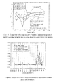
- Figure 1 compares the ellipsometry spectra obtained through the depositions with HMDSO with the undoped and 'p' type doped a-SiOx:H films. As seen in Figure 1 , the intensity of ellipsometry spectra from the 'p' type a-SiOx:H films obtained from HMDSO as the oxygen source decreases as HMDSO flow rate increases. This indicates that the Oxygen content in the films is increasing.
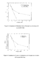
- Figure 2 compares the FTIR spectra of the depositions in different gas mixture conditions.
- the FTIR spectra of the p type a-Si:H films, p type a-SiOx:H films from CO 2 and p type a-SiOx:H films from HMDSO is shown.
- the presence of a peak ( ⁇ 1200 cm -1 ) in FTIR spectra indicates the presence of Si-O. This peak is seen in the FTIR spectra of SiO 2 films, p-a-SiOx:H from CO 2 as Oxygen source and p-a-SiOx:H from HMDSO as the Oxygen source.
- the described Si-O-Si molecules of the invention presents a new method to deposit undoped and doped amorphous silicon oxide (a-SiOx:H) film on a substrate surface.
- These films have superior properties (refractive index, optical band gap, conductivity, mechanical and material) than the conventional films deposited from other oxygen sources like water, oxygen, N 2 O and CO 2 . These enhanced properties will facilitate the increased efficiencies of the solar cells.
- Example 2 - p-type amorphous silicon oxide layers using HMDSO as the Oxygen source.
- the doped layers (p-type and n-type) in thin film silicon solar cells are necessary to provide an electron-hole separation mechanism. These layers are a source of parasitic absorption, but can provide an advantage if they provide greater control over optical reflection.
- Hexamethyldisiloxane C 6 H 18 OSi 2 , HMDSO
- HMDSO Hexamethyldisiloxane
- the use of molecules with pre-formed Si-O-Si bonds as the oxygen source growth precursor is expected to provide different material properties as compared to when the Oxygen arrives as either an atom or as a hydroxyl group (-OH).
- CO 2 is used as the Oxygen source for depositing p-type a-SiOx:H layers.
- p-a-SiOx:H layers were deposited on glass substrate (AF-32) and FZ Wafer.
- the refractive index (n) of the layers was estimated by fitting the Ellipsometry curves on Delta-Psi2 software.
- the coplanar conductivities were evaluated by evaporating metal contacts on the deposited layers and measuring the current at a specified voltage.
- the bond configuration in the films was confirmed with Fourier Transform Infrared Spectroscopy (FTIR).
- FTIR Fourier Transform Infrared Spectroscopy
- SIMS Secondary Ion Mass Spectroscopy
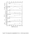
- Figure 3 shows the comparison of Refractive Index (n) of the layers as a function of Oxygen source/SiH 4 flow.
- the Oxygen source is HMDSO in one case and CO 2 in another case.
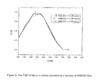
- Figure 4 shows the comparison of coplanar conductivities of the layers as a function of Oxygen source/SiH 4 flow.
Landscapes
- Chemical Vapour Deposition (AREA)
- Photovoltaic Devices (AREA)
Priority Applications (1)
| Application Number | Priority Date | Filing Date | Title |
|---|---|---|---|
| EP14305830.3A EP2953155A1 (de) | 2014-06-02 | 2014-06-02 | Verwendung von Si-O-Si-basierten Molekülen zur Ablagerung einer amorphen Siliciumoxidschicht auf einem Substrat |
Applications Claiming Priority (1)
| Application Number | Priority Date | Filing Date | Title |
|---|---|---|---|
| EP14305830.3A EP2953155A1 (de) | 2014-06-02 | 2014-06-02 | Verwendung von Si-O-Si-basierten Molekülen zur Ablagerung einer amorphen Siliciumoxidschicht auf einem Substrat |
Publications (1)
| Publication Number | Publication Date |
|---|---|
| EP2953155A1 true EP2953155A1 (de) | 2015-12-09 |
Family
ID=50942242
Family Applications (1)
| Application Number | Title | Priority Date | Filing Date |
|---|---|---|---|
| EP14305830.3A Withdrawn EP2953155A1 (de) | 2014-06-02 | 2014-06-02 | Verwendung von Si-O-Si-basierten Molekülen zur Ablagerung einer amorphen Siliciumoxidschicht auf einem Substrat |
Country Status (1)
| Country | Link |
|---|---|
| EP (1) | EP2953155A1 (de) |
Cited By (1)
| Publication number | Priority date | Publication date | Assignee | Title |
|---|---|---|---|---|
| EP2953154A1 (de) * | 2014-06-02 | 2015-12-09 | L'air Liquide, Societe Anonyme Pour L'etude Et L'exploitation Des Procedes Georges Claude | Verwendung von Si-O-Si-basierten Molekülen für hocheffiziente Si-Solarzellen |
Citations (4)
| Publication number | Priority date | Publication date | Assignee | Title |
|---|---|---|---|---|
| EP1006569A2 (de) * | 1998-12-04 | 2000-06-07 | Canon Sales Co., Inc. | Abscheidung eines isolierenden Films |
| US20040033373A1 (en) * | 1998-04-28 | 2004-02-19 | Peter Rose | Low kappa dielectric inorganic/organic hybrid films and methods of making |
| US7217658B1 (en) * | 2004-09-07 | 2007-05-15 | Novellus Systems, Inc. | Process modulation to prevent structure erosion during gap fill |
| EP2953154A1 (de) * | 2014-06-02 | 2015-12-09 | L'air Liquide, Societe Anonyme Pour L'etude Et L'exploitation Des Procedes Georges Claude | Verwendung von Si-O-Si-basierten Molekülen für hocheffiziente Si-Solarzellen |
-
2014
- 2014-06-02 EP EP14305830.3A patent/EP2953155A1/de not_active Withdrawn
Patent Citations (4)
| Publication number | Priority date | Publication date | Assignee | Title |
|---|---|---|---|---|
| US20040033373A1 (en) * | 1998-04-28 | 2004-02-19 | Peter Rose | Low kappa dielectric inorganic/organic hybrid films and methods of making |
| EP1006569A2 (de) * | 1998-12-04 | 2000-06-07 | Canon Sales Co., Inc. | Abscheidung eines isolierenden Films |
| US7217658B1 (en) * | 2004-09-07 | 2007-05-15 | Novellus Systems, Inc. | Process modulation to prevent structure erosion during gap fill |
| EP2953154A1 (de) * | 2014-06-02 | 2015-12-09 | L'air Liquide, Societe Anonyme Pour L'etude Et L'exploitation Des Procedes Georges Claude | Verwendung von Si-O-Si-basierten Molekülen für hocheffiziente Si-Solarzellen |
Non-Patent Citations (2)
| Title |
|---|
| KOBSAK SRIPRAPHA ET AL: "p-Type hydrogenated silicon oxide thin film deposited near amorphous to microcrystalline phase transition and its application to solar cells", CURRENT APPLIED PHYSICS, NORTH-HOLLAND, AMSTERDAM, NL, vol. 11, no. 1, 1 November 2010 (2010-11-01), pages S47 - S49, XP028156911, ISSN: 1567-1739, [retrieved on 20101105], DOI: 10.1016/J.CAP.2010.11.008 * |
| SMIRNOV V. ET AL: "Microcrystalline silicon oxide (uc-SiOx:H) alloys: A versatile material for application in thin film silicon single and tandem junction solar cells", JOURNAL OF NON-CRYSTALLINE SOLIDS, no. 358, 30 December 2011 (2011-12-30), pages 1954 - 1957, XP002727953, DOI: 10.1016/j.jnoncrysol.2011.12.019 * |
Cited By (1)
| Publication number | Priority date | Publication date | Assignee | Title |
|---|---|---|---|---|
| EP2953154A1 (de) * | 2014-06-02 | 2015-12-09 | L'air Liquide, Societe Anonyme Pour L'etude Et L'exploitation Des Procedes Georges Claude | Verwendung von Si-O-Si-basierten Molekülen für hocheffiziente Si-Solarzellen |
Similar Documents
| Publication | Publication Date | Title |
|---|---|---|
| CN102044632B (zh) | 用于cigs电池的氧化锌膜方法和结构 | |
| US20110126893A1 (en) | Thin film silicon solar cell and manufacturing method thereof | |
| JP2010067973A (ja) | 薄膜の微結晶シリコン合金及びウエハベースのソーラー用途 | |
| US20150136210A1 (en) | Silicon-based solar cells with improved resistance to light-induced degradation | |
| US20120325302A1 (en) | Photovoltaic device including flexible or inflexible substrate and method for manufacturing the same | |
| US20120202315A1 (en) | In-situ hydrogen plasma treatment of amorphous silicon intrinsic layers | |
| KR20250163403A (ko) | 태양 전지 및 그 제조 방법 | |
| CN102656707B (zh) | 薄膜硅叠层太阳能电池及其制造方法 | |
| US20110308583A1 (en) | Plasma treatment at a p-i junction for increasing open circuit voltage of a photovoltaic device | |
| Pandey et al. | Investigation of dual intrinsic a-Si: H films for crystalline silicon surface passivation by spectroscopic ellipsometry: application in silicon heterojunction solar cells | |
| EP2953154A1 (de) | Verwendung von Si-O-Si-basierten Molekülen für hocheffiziente Si-Solarzellen | |
| US4738729A (en) | Amorphous silicon semiconductor solar cell | |
| EP2953155A1 (de) | Verwendung von Si-O-Si-basierten Molekülen zur Ablagerung einer amorphen Siliciumoxidschicht auf einem Substrat | |
| US20110232753A1 (en) | Methods of forming a thin-film solar energy device | |
| JP2024109826A (ja) | シングル型、タンデム型ならびにヘテロ接合型太陽電池装置およびその形成方法 | |
| Ide et al. | Amorphous silicon thin films prepared by hot wire cell method and its application to solar cells | |
| Woerdenweber et al. | Incorporation and critical concentration of oxygen in a-Si: H solar cells | |
| Lee et al. | Characterization of microcrystalline silicon thin film solar cells prepared by high working pressure plasma-enhanced chemical vapor deposition | |
| EP2953156A1 (de) | Verwendung von TMDSO zur Abscheidung einer Siliciumdioxidschicht auf ein Substrat | |
| CN103022245A (zh) | 用于光伏钝化的含氧前体 | |
| JP2726676B2 (ja) | シリコンカーバイド微結晶薄膜の形成法 | |
| JPH06260665A (ja) | 非晶質太陽電池 | |
| Kaur et al. | Development of n-type, Passivating Nanocrystalline Silicon Oxide (nc-SiOx: H) Films via PECVD | |
| JP2004297008A (ja) | p型半導体材料、その作製方法、その作製装置、光電変換素子、発光素子、および薄膜トランジスタ | |
| Boldyryeva et al. | Characterization of hydrogen contained in passivated poly‐Si and microcrystalline‐Si by ERDA technique |
Legal Events
| Date | Code | Title | Description |
|---|---|---|---|
| PUAI | Public reference made under article 153(3) epc to a published international application that has entered the european phase |
Free format text: ORIGINAL CODE: 0009012 |
|
| AK | Designated contracting states |
Kind code of ref document: A1 Designated state(s): AL AT BE BG CH CY CZ DE DK EE ES FI FR GB GR HR HU IE IS IT LI LT LU LV MC MK MT NL NO PL PT RO RS SE SI SK SM TR |
|
| AX | Request for extension of the european patent |
Extension state: BA ME |
|
| 17P | Request for examination filed |
Effective date: 20160609 |
|
| RBV | Designated contracting states (corrected) |
Designated state(s): AL AT BE BG CH CY CZ DE DK EE ES FI FR GB GR HR HU IE IS IT LI LT LU LV MC MK MT NL NO PL PT RO RS SE SI SK SM TR |
|
| 17Q | First examination report despatched |
Effective date: 20191211 |
|
| STAA | Information on the status of an ep patent application or granted ep patent |
Free format text: STATUS: THE APPLICATION IS DEEMED TO BE WITHDRAWN |
|
| 18D | Application deemed to be withdrawn |
Effective date: 20200623 |