EP2050140B1 - Verfahren zur herstellung eines doppelgate-transistors - Google Patents
Verfahren zur herstellung eines doppelgate-transistors Download PDFInfo
- Publication number
- EP2050140B1 EP2050140B1 EP07805282A EP07805282A EP2050140B1 EP 2050140 B1 EP2050140 B1 EP 2050140B1 EP 07805282 A EP07805282 A EP 07805282A EP 07805282 A EP07805282 A EP 07805282A EP 2050140 B1 EP2050140 B1 EP 2050140B1
- Authority
- EP
- European Patent Office
- Prior art keywords
- semiconductor layer
- amorphous
- layer
- amorphous semiconductor
- crystalline semiconductor
- Prior art date
- Legal status (The legal status is an assumption and is not a legal conclusion. Google has not performed a legal analysis and makes no representation as to the accuracy of the status listed.)
- Not-in-force
Links
Images


Classifications
-
- H—ELECTRICITY
- H10—SEMICONDUCTOR DEVICES; ELECTRIC SOLID-STATE DEVICES NOT OTHERWISE PROVIDED FOR
- H10P—GENERIC PROCESSES OR APPARATUS FOR THE MANUFACTURE OR TREATMENT OF DEVICES COVERED BY CLASS H10
- H10P14/00—Formation of materials, e.g. in the shape of layers or pillars
- H10P14/20—Formation of materials, e.g. in the shape of layers or pillars of semiconductor materials
- H10P14/29—Formation of materials, e.g. in the shape of layers or pillars of semiconductor materials characterised by the substrates
- H10P14/2901—Materials
- H10P14/2902—Materials being Group IVA materials
- H10P14/2905—Silicon, silicon germanium or germanium
-
- H—ELECTRICITY
- H10—SEMICONDUCTOR DEVICES; ELECTRIC SOLID-STATE DEVICES NOT OTHERWISE PROVIDED FOR
- H10D—INORGANIC ELECTRIC SEMICONDUCTOR DEVICES
- H10D30/00—Field-effect transistors [FET]
- H10D30/01—Manufacture or treatment
- H10D30/021—Manufacture or treatment of FETs having insulated gates [IGFET]
- H10D30/031—Manufacture or treatment of FETs having insulated gates [IGFET] of thin-film transistors [TFT]
- H10D30/0321—Manufacture or treatment of FETs having insulated gates [IGFET] of thin-film transistors [TFT] comprising silicon, e.g. amorphous silicon or polysilicon
- H10D30/0323—Manufacture or treatment of FETs having insulated gates [IGFET] of thin-film transistors [TFT] comprising silicon, e.g. amorphous silicon or polysilicon comprising monocrystalline silicon
-
- H—ELECTRICITY
- H10—SEMICONDUCTOR DEVICES; ELECTRIC SOLID-STATE DEVICES NOT OTHERWISE PROVIDED FOR
- H10D—INORGANIC ELECTRIC SEMICONDUCTOR DEVICES
- H10D30/00—Field-effect transistors [FET]
- H10D30/60—Insulated-gate field-effect transistors [IGFET]
- H10D30/67—Thin-film transistors [TFT]
- H10D30/6729—Thin-film transistors [TFT] characterised by the electrodes
- H10D30/673—Thin-film transistors [TFT] characterised by the electrodes characterised by the shapes, relative sizes or dispositions of the gate electrodes
- H10D30/6733—Multi-gate TFTs
- H10D30/6734—Multi-gate TFTs having gate electrodes arranged on both top and bottom sides of the channel, e.g. dual-gate TFTs
-
- H—ELECTRICITY
- H10—SEMICONDUCTOR DEVICES; ELECTRIC SOLID-STATE DEVICES NOT OTHERWISE PROVIDED FOR
- H10P—GENERIC PROCESSES OR APPARATUS FOR THE MANUFACTURE OR TREATMENT OF DEVICES COVERED BY CLASS H10
- H10P14/00—Formation of materials, e.g. in the shape of layers or pillars
- H10P14/20—Formation of materials, e.g. in the shape of layers or pillars of semiconductor materials
- H10P14/34—Deposited materials, e.g. layers
- H10P14/3402—Deposited materials, e.g. layers characterised by the chemical composition
- H10P14/3404—Deposited materials, e.g. layers characterised by the chemical composition being Group IVA materials
- H10P14/3411—Silicon, silicon germanium or germanium
-
- H—ELECTRICITY
- H10—SEMICONDUCTOR DEVICES; ELECTRIC SOLID-STATE DEVICES NOT OTHERWISE PROVIDED FOR
- H10P—GENERIC PROCESSES OR APPARATUS FOR THE MANUFACTURE OR TREATMENT OF DEVICES COVERED BY CLASS H10
- H10P14/00—Formation of materials, e.g. in the shape of layers or pillars
- H10P14/20—Formation of materials, e.g. in the shape of layers or pillars of semiconductor materials
- H10P14/38—Formation of materials, e.g. in the shape of layers or pillars of semiconductor materials characterised by treatments done after the formation of the materials
-
- H—ELECTRICITY
- H10—SEMICONDUCTOR DEVICES; ELECTRIC SOLID-STATE DEVICES NOT OTHERWISE PROVIDED FOR
- H10P—GENERIC PROCESSES OR APPARATUS FOR THE MANUFACTURE OR TREATMENT OF DEVICES COVERED BY CLASS H10
- H10P14/00—Formation of materials, e.g. in the shape of layers or pillars
- H10P14/20—Formation of materials, e.g. in the shape of layers or pillars of semiconductor materials
- H10P14/38—Formation of materials, e.g. in the shape of layers or pillars of semiconductor materials characterised by treatments done after the formation of the materials
- H10P14/3802—Crystallisation or recrystallisation of non-monocrystalline semiconductor materials, e.g. regrowth
- H10P14/3804—Crystallisation or recrystallisation of non-monocrystalline semiconductor materials, e.g. regrowth using crystallisation-inhibiting elements
Definitions
- the invention relates to a method of manufacturing a double gate transistor comprising a channel region and two gate electrodes disposed on opposing sides of the channel region.
- MOSFETs Metal-oxide-semiconductor field-effect transistors
- US-B-6,593,192 discloses an example method of forming a dual-gate semiconductor-on-insulator (SOI) device in which a first gate is aligned with a second gate, each being formed on opposing sides of a semiconductor layer.
- first gate structures are formed over active areas before a handle wafer is bonded to the upper surface of the structure and the bulk substrate is removed to expose the insulator layer.
- portions of the insulator layer 20 are removed to form openings 26 between adjacent source and drain contact structures 58.
- Second transistor gate structures 95 are then formed within the openings 26, as shown in Figure 9 of US-6,593,192 .
- This method involves a transfer of the device onto a second carrier substrate which allows the subsequent processing of the second side of the channel leading to the forming of the second gate.
- the substrate transfer requires many process steps thus adding to the time and cost associated with the manufacture. Furthermore, in order to accurately align the two gates with one another, several process steps are required which adds to the expense further still.
- WO2004/088757 discloses a method of fabricating a double gate transistor.
- a lower gate electrode is formed in a cavity obtained by removal of an embedded insulating film.
- Part of the insulating film is maintained below the source and drain regions to isolate them from the lower gate.
- the part to be maintained is implanted with a dopant introduced through the source and drain regions to provide etch selectivity with respect to the undoped part prior to removal of the embedded insulating film.
- a method of manufacturing a double gate transistor comprising a channel region and two gate electrodes disposed on opposing sides of the channel region, the method comprising the steps of providing a semiconductor wafer with a laminate structure comprising an initial crystalline semiconductor layer on an amorphous semiconductor layer, wherein the initial crystalline semiconductor layer comprises a channel region; introducing crystallisation inhibitors into a selected region of the semiconductor wafer, said selected region extending through the amorphous semiconductor layer in a position corresponding to the lateral position of the channel region; performing a crystallisation operation so as to crystallise regions of the amorphous semiconductor layer outside of the selected region thereby forming a developed crystalline semiconductor layer having a greater thickness than that of said initial crystalline semiconductor layer away from said selected region and a substantially similar thickness to that of said initial crystalline semiconductor layer within the selected region; selectively removing remaining amorphous semiconductor material to form a cavity below the developed crystalline semiconductor layer; and, forming a lower gate electrode under the channel region within the cavity and an
- the introducing of crystallisation inhibitors within the channel region provides a simple route to tailoring the channel thickness by means of epitaxial regrowth of the crystalline semiconductor. Whilst the areas outside of the selected region are grown, e.g. to form more substantial source/drain extensions, the growth of the channel is limited thus resulting in a thin gate which ensures electrostatic device integrity.
- the laminate structure may comprise a further amorphous semiconductor layer adjacent the major surface of the initial crystalline semiconductor layer remote said amorphous semiconductor layer, and the selected region extending through both amorphous semiconductor layers, and wherein the crystallisation step serves also to crystallise regions of the further amorphous semiconductor layer outside of the selected region.
- the channel can, advantageously, be thinned from both sides.
- the crystallisation inhibitors are introduced through the thickness of the laminate structure thus limiting the regrowth of the crystalline channel region. It will be appreciated that the thickness of the crystalline semiconductor layer between the two amorphous layers essentially determines the thickness of the channel in the final device.
- the amorphous layer, or layers can be provided by amorphizing a layer within a crystalline semiconductor substrate. Preferably this is done by implanting ions into a major surface of the crystalline semiconductor substrate. In the case of the laminate structure comprising two amorphous layers separated by the crystalline semiconductor layer, ions are implanted at two different energies to amorphize the layer at two different depths within the crystalline semiconductor substrate.
- the step of introducing crystallisation inhibitors may be carried out before said step of amorphizing.
- the step of providing a semiconductor wafer includes depositing an amorphous semiconductor layer on a crystalline semiconductor substrate. This avoids the need for the deep underlying amorphisation steps and allows less damage in the crystalline layer and more accurate control of the layer thickness by more controllable epitaxial deposition for example.
- the crystallisation inhibitors preferably comprise fluorine ions, but may alternatively comprise carbon or nitrogen.
- the step of introducing crystallisation inhibitors may comprise the steps of depositing a mask layer over the semiconductor wafer; patterning the mask layer to expose a region of the semiconductor wafer surface; and, implanting the crystallisation inhibitors into the semiconductor wafer.
- the amorphous semiconductor layer(s) are preferably crystallised by performing a solid phase epitaxial regrowth of the amorphous semiconductor layer(s) by heating the laminate structure to a temperature in the range of 550C to 600C for example.
- the thickness of the crystalline semiconductor layer outside of the channel is determined by this process.
- the invention involves the processing of a semiconductor wafer.
- a semiconductor wafer 10 of crystalline silicon in this case, is provided and supported in a manner conventional with CMOS technology. It should be appreciated that the figures show in section only a very small portion of the wafer and that many devices are typically processed on the same wafer. Furthermore, the invention is not limited to silicon and the semiconductor may alternatively be of Ge, SiGe or GaAs for example.
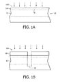
- a major surface, the top surface in this example, of the silicon substrate 10 is subjected to an implantation of germanium ions 100 to amorphize a layer 12 at a predetermined depth within the substrate 10.
- the energy of the ion implant can be adjusted to tune the thickness and depth of the amorphous layer 12.
- the implantation is carried out at an energy of around 30-200keV and at a dosage within the range of 1e13 to 4e14 atoms/cm 2 .
- Si, Ar or Xe ions can be used instead of germanium.
- the result of the amorphisation is a semiconductor wafer having a laminate structure comprising a crystalline semiconductor layer 14 which comprises a channel region 16, adjacent an amorphous semiconductor layer 12.
- a masking layer 18 is deposited on the substrate 10.
- the masking layer is a commercially available polymer photoresist.
- This mask layer 18 is then patterned (as shown in Figure 1 B) to expose a region in the wafer surface.
- the exposed region is rectangular in shape but may be any shape to fit the purpose, e.g. circular.
- crystallisation inhibitors are implanted into the semiconductor wafer 10.
- the crystallisation inhibitors comprise fluorine ions and are implanted at a dose within the range of 5e14 to 2e15 atoms/cm 2 and having an energy of 2-15keV.
- the masking layer 18 prevents the fluorine ions from hitting the masked region of the wafer 10.
- the fluorine ions are only introduced into a selected region 20 of the wafer 10, the selected region 20 extending through the amorphous semiconductor layer 12 in a position corresponding to the lateral position of the channel region 16.
- other crystallisation inhibitors can instead be employed such as O, N, C, and Cl for example.
- the masking layer 18 is then removed in a known manner.
- a crystallisation operation is then carried out so as to crystallise regions of the amorphous semiconductor layer 12 outside of the selected region 20.
- a solid phase epitaxial regrowth of the amorphous semiconductor layer 12 is carried out by heating the laminate structure 10 to a temperature in the range of 550C to 600C.
- the presence of the crystallisation inhibiters within the selected region 20 serves to slow down the rate of recrystallisation within the selected region. Therefore, the amorphous silicon layer 12 outside the selected region 20 recrystallises faster than that within the selected region by a factor of five to ten times.
- the result is a developed crystalline semiconductor layer 14' having a greater thickness than that of said initial crystalline semiconductor layer 14 away from said selected region 20.
- the developed crystalline semiconductor layer 14' within the selected region 20 has a substantially similar thickness to that of said initial crystalline semiconductor layer 14 as illustrated in Figure 1C .
- the thinner part of the developed crystalline silicon layer 14' will eventually form the channel of the double gate transistor.
- the invention allows the fabrication of a semiconductor layer having a region of reduced thickness for the gate-controlled electron channel whilst also having regions of greater thickness for the low-resistivity source/drain extensions.
- the simplicity of the processing associated with the use of the crystallisation inhibitors makes the process very attractive for introduction in existing CMOS process flows in which the introduction of new and expensive apparatus would not be required.
- the remaining amorphous semiconductor material of the amorphous semiconductor layer 12 (now of reduced thickness) is selectively removed by performing a wet etch using HF acid for example.
- the result is a cavity 22 below the developed crystalline layer 14'.
- Access holes/trenches (not shown) are formed through the developed crystalline layer 14' to enable access to the amorphous layer, and eventually to the cavity, through a major surface of the wafer 10.
- Gate dielectric layers 24 and 26 are formed on the upper and lower surfaces of the developed crystalline layer 14' respectively. This may be done by heating the structure in an oxidising ambient such that the lower dielectric layer is formed via the access holes.
- the gate dielectric layers 24 and 26 are approximately 1.5nm in thickness and serve to insulate the gates from the channel region 16.
- the cavity 22 is then filled with a metal such as TiN through the access holes (not shown).
- a metal such as TiN
- This metal is patterned using a timed wet etch [correct] to leave a lower gate 30 positioned under the channel region 16 within the cavity 22. Connections to the lower gate 30 may, for example, be made through the access trenches.
- the upper gate 32 is formed using known lithographic techniques which may include a metal deposition which is then patterned.
- the invention provides a simple wafer-based process to fabricate a planar double-gate device having a channel region which is significantly thinner than the source/drain extensions provided in the same semiconductor layer.
- the order in which the process steps are carried out is flexible to a certain extent.
- the crystallisation inhibitors may be introduced at an earlier stage, as is the case in the second embodiment described which will now be described.
- a masking layer 18 is deposited over a crystalline silicon wafer 10 and patterned to expose a region of the wafer surface as shown in Figure 2A . Fluorine ions are then implanted into a selected region 20 of the semiconductor wafer as defined by the patterned mask 18, and which process is referenced at 200. Conditions for the implant are similar to those described for the first embodiment.
- a wafer-wide amorphizing implant 100 is then carried out at two different energies to amorphize two layers of different depths within the crystalline wafer 10. For example, one set of germanium ions is implanted at an energy of 30-200keV to amorphize a layer 12 at a depth of around 20nm down to a depth of 60nm as shown in Figure 2B . The position of the deep amorphous layer will depend on the desired channel thickness and the top amorphous layer. A second set of germanium ions is implanted at a lower energy to create an amorphous layer 13 near the top surface of the wafer 10.
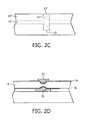
- the laminate structure is then heated so as to partially re-grow the amorphous silicon layers 12,13, to a much greater extent outside of the fluorine-implanted region 20 than within.
- the regrowth occurs at the major surfaces of the crystalline silicon layer 14 which are in contact with the amorphous silicon layers 12, 13.
- the crystalline silicon layer 14 grows so that its thickness increases.
- the growth is restricted within the fluorine-implanted region 20 so that the developed crystalline silicon layer 14' has a corresponding area of reduced thickness 16 in which the channel of the final double-gate device will be located.
- the re-growth of the channel region 16 is restricted in two directions which allows for an even thinner channel region relative to the thickness of the source/drain extension regions.
- the re-grown, or developed, crystalline silicon layer 14' can be seen in Figure 2C , together with the remaining parts of the amorphous silicon layers 12',13'.
- the subsequent processing does not differ significantly from the first-described embodiment.
- the remaining amorphous silicon material 12',13' is selectively removed by a wet etch, employing access trenches (not shown) in the wafer's major surface, thus leaving a cavity under the developed crystalline silicon layer.
- the upper and lower gate dielectric layers 24, 26 are formed in the same way as before. Also, the upper and lower metallic gates 32, 30 are formed in a similar manner.
- the above-described embodiment employs amorphisation of a crystalline semiconductor wafer to form the two amorphous layers in the laminate structure
- other techniques such as deposition.
- the laminate structure may be built up with a series of deposition steps.
- one amorphous layer may be formed by amorphisation and the other by deposition.
- a planar double-gate transistor wherein crystallisation inhibitors are implanted into the channel region of a semiconductor wafer, said wafer having a laminate structure comprising an initial crystalline semiconductor layer adjacent an amorphous semiconductor layer.
- Upon heating, partial re-growth of the amorphous semiconductor layer is restricted in the channel area thus allowing for the thickness of the source/drain extension regions to be increased whilst maintaining a thin channel. Any remaining amorphous material is selectively removed leaving a cavity to allow for the forming of gate electrodes on opposing sides of the channel region.
- the invention can be exploited to a greater extent by providing an amorphous layer on both sides of the initial crystalline semiconductor layer thus providing for re-growth limitation in two directions.
Landscapes
- Recrystallisation Techniques (AREA)
- Thin Film Transistor (AREA)
- Metal-Oxide And Bipolar Metal-Oxide Semiconductor Integrated Circuits (AREA)
- Bipolar Transistors (AREA)
Claims (12)
- Verfahren zur Herstellung eines Doppelgate-Transistors, der ein Kanalgebiet (16) und zwei Gate-Elektroden (30, 32), die auf gegenüberliegenden Seiten des Kanalgebiets angeordnet sind, umfasst, wobei das Verfahren die Schritte umfasst:Bereitstellen eines Halbleiter-Wafers (10) mit einer Laminatstruktur, die eine anfängliche kristalline Halbleiterschicht (14) auf einer amorphen Halbleiterschicht (12) umfasst, wobei die anfängliche kristalline Halbleiterschicht (14) ein Kanalgebiet umfasst;Einbringen von Kristallisationshemmstoffen (200) in ein ausgewähltes Gebiet (20) des Halbleiter-Wafers, wobei sich das ausgewählte Gebiet durch die amorphe Halbleiterschicht an einer Position erstreckt, die der lateralen Position des Kanalgebiets entspricht;Durchführen eines Kristallisationsvorgangs, um somit Gebiete der amorphen Halbleiterschicht außerhalb des ausgewählten Gebiets zu kristallisieren, um somit eine entwickelte kristalline Halbleiterschicht (14') zu bilden, die eine größere Dicke als die anfängliche kristalline Halbleiterschicht (14) entfernt von dem ausgewählten Gebiet und eine im Wesentlichen ähnliche Dicke wie die anfängliche kristalline Halbleiterschicht innerhalb des ausgewählten Gebiets aufweist;selektives Entfernen von restlichem amorphem Halbleitermaterial, um einen Hohlraum unterhalb der entwickelten kristallinen Halbleiterschicht (14') zu bilden; undBilden einer unteren Gate-Elektrode (30) unter dem Kanalgebiet (16) innerhalb des Hohlraums (22) und einer oberen Gate-Elektrode (32) über dem Kanalgebiet (16) gegenüberliegend der unteren Gate-Elektrode (30).
- Verfahren nach Anspruch 1, wobei die Laminatstruktur eine weitere amorphe Halbleiterschicht (13) benachbart zur Hauptoberfläche der anfänglichen kristallinen Halbleiterschicht fern der amorphen Halbleiterschicht (12) umfasst, wobei sich das ausgewählte Gebiet durch beide amorphen Halbleiterschichten erstreckt, und wobei der Kristallisierungsschritt auch dazu dient, Gebiete der weiteren amorphen Halbleiterschicht außerhalb des ausgewählten Gebiets zu kristallisieren.
- Verfahren nach Anspruch 1 oder 2, wobei der Schritt des Bereitstellens eines Halbleiter-Wafers enthält:Amorphisieren einer Schicht innerhalb eines kristallinen Halbleitersubstrats, um die amorphe Halbleiterschicht zu bilden.
- Verfahren nach Anspruch 3, wobei das Amorphisieren das Implantieren von Ionen in eine Hauptoberfläche des kristallinen Halbleitersubstrats umfasst.
- Verfahren nach Anspruch 2, wobei der Schritt des Bereitstellens eines Halbleiter-Wafers enthält:Amorphisieren von zwei Schichten mit unterschiedlichen Tiefen innerhalb des kristallinen Halbleitersubstrats durch Implantieren von Ionen in eine Hauptoberfläche des kristallinen Halbleitersubstrats mit zwei unterschiedlichen Energien, um somit beide amorphen Halbleiterschichten (12, 13) zu bilden.
- Verfahren nach irgendeinem der Ansprüche 3 bis 5, wobei der Schritt des Einbringens von Kristallisationshemmstoffen vor dem Schritt des Amorphisierens ausgeführt wird.
- Verfahren nach irgendeinem der Ansprüche 1 bis 4, wobei der Schritt des Bereitstellens eines Halbleiter-Wafers enthält:Abscheiden einer amorphen Halbleiterschicht auf einem kristallinen Halbleitersubstrat.
- Verfahren nach irgendeinem der vorangehenden Ansprüche, wobei die Kristallisationshemmstoffe Fluorionen umfassen.
- Verfahren nach irgendeinem der vorangehenden Ansprüche, wobei der Schritt des Einbringens von Kristallisationshemmstoffen die Schritte umfasst:Abscheiden einer Maskenschicht (18) über dem Halbleiter-Wafer;Strukturieren der Maskenschicht, um ein Gebiet der Halbleiter-Wafer-Oberfläche freizulegen; undImplantieren der Kristallisationshemmstoffe in den Halbleiter-Wafer.
- Verfahren nach irgendeinem der vorangehenden Ansprüche, wobei der Schritt des Kristallisierens eines Teils der amorphen Halbleiterschicht(en) das Ausführen eines Feststoffphase-Epitaxie-Neuwachstums der amorphen Halbleiterschicht(en) umfasst.
- Verfahren nach Anspruch 10, wobei das Feststoffphase-Epitaxie-Neuwachstum das Erwärmen der Laminatstruktur auf eine Temperatur im Bereich von 550 °C bis 600 °C enthält.
- Verfahren nach irgendeinem der vorangehenden Ansprüche, wobei der Schritt des selektiven Entfernens von restlichem amorphem Halbleitermaterial das Durchführen eines Nassätzens umfasst.
Priority Applications (1)
| Application Number | Priority Date | Filing Date | Title |
|---|---|---|---|
| EP07805282A EP2050140B1 (de) | 2006-08-04 | 2007-08-01 | Verfahren zur herstellung eines doppelgate-transistors |
Applications Claiming Priority (3)
| Application Number | Priority Date | Filing Date | Title |
|---|---|---|---|
| EP06118448 | 2006-08-04 | ||
| EP07805282A EP2050140B1 (de) | 2006-08-04 | 2007-08-01 | Verfahren zur herstellung eines doppelgate-transistors |
| PCT/IB2007/053036 WO2008015649A1 (en) | 2006-08-04 | 2007-08-01 | Method of manufacturing a double gate transistor |
Publications (2)
| Publication Number | Publication Date |
|---|---|
| EP2050140A1 EP2050140A1 (de) | 2009-04-22 |
| EP2050140B1 true EP2050140B1 (de) | 2010-05-12 |
Family
ID=38792440
Family Applications (1)
| Application Number | Title | Priority Date | Filing Date |
|---|---|---|---|
| EP07805282A Not-in-force EP2050140B1 (de) | 2006-08-04 | 2007-08-01 | Verfahren zur herstellung eines doppelgate-transistors |
Country Status (6)
| Country | Link |
|---|---|
| US (1) | US8183116B2 (de) |
| EP (1) | EP2050140B1 (de) |
| CN (1) | CN101501861B (de) |
| AT (1) | ATE467908T1 (de) |
| DE (1) | DE602007006507D1 (de) |
| WO (1) | WO2008015649A1 (de) |
Families Citing this family (2)
| Publication number | Priority date | Publication date | Assignee | Title |
|---|---|---|---|---|
| US10043676B2 (en) * | 2015-10-15 | 2018-08-07 | Vishay General Semiconductor Llc | Local semiconductor wafer thinning |
| CN108767011A (zh) * | 2018-04-28 | 2018-11-06 | 南京邮电大学 | 一种双栅mosfet结构 |
Family Cites Families (14)
| Publication number | Priority date | Publication date | Assignee | Title |
|---|---|---|---|---|
| JP2595525B2 (ja) * | 1987-04-10 | 1997-04-02 | ソニー株式会社 | 半導体薄膜の形成方法 |
| US6593192B2 (en) * | 2001-04-27 | 2003-07-15 | Micron Technology, Inc. | Method of forming a dual-gated semiconductor-on-insulator device |
| US6661044B2 (en) * | 2001-10-22 | 2003-12-09 | Winbond Electronics Corp. | Method of manufacturing MOSEFT and structure thereof |
| JP2003318405A (ja) * | 2002-04-25 | 2003-11-07 | Mitsubishi Electric Corp | 半導体装置およびその製造方法 |
| JP2003332582A (ja) * | 2002-05-13 | 2003-11-21 | Toshiba Corp | 半導体装置及びその製造方法 |
| CN1224087C (zh) * | 2002-08-26 | 2005-10-19 | 中国科学院微电子中心 | 凹槽平面双栅结构mos器件及制造方法 |
| JP4178296B2 (ja) * | 2003-03-28 | 2008-11-12 | 富士通マイクロエレクトロニクス株式会社 | 半導体装置及びその製造方法 |
| US6838329B2 (en) * | 2003-03-31 | 2005-01-04 | Intel Corporation | High concentration indium fluorine retrograde wells |
| US6936505B2 (en) * | 2003-05-20 | 2005-08-30 | Intel Corporation | Method of forming a shallow junction |
| US7019342B2 (en) * | 2003-07-03 | 2006-03-28 | American Semiconductor, Inc. | Double-gated transistor circuit |
| US7018873B2 (en) * | 2003-08-13 | 2006-03-28 | International Business Machines Corporation | Method of making a device threshold control of front-gate silicon-on-insulator MOSFET using a self-aligned back-gate |
| JP2007504660A (ja) * | 2003-09-03 | 2007-03-01 | コーニンクレッカ フィリップス エレクトロニクス エヌ ヴィ | ダブルゲート電界効果トランジスタ装置を製造する方法、及びそのようなダブルゲート電界効果トランジスタ装置 |
| US7923782B2 (en) * | 2004-02-27 | 2011-04-12 | International Business Machines Corporation | Hybrid SOI/bulk semiconductor transistors |
| GB0411621D0 (en) * | 2004-05-25 | 2004-06-30 | Koninkl Philips Electronics Nv | Dual gate semiconductor device |
-
2007
- 2007-08-01 DE DE602007006507T patent/DE602007006507D1/de active Active
- 2007-08-01 AT AT07805282T patent/ATE467908T1/de not_active IP Right Cessation
- 2007-08-01 CN CN200780028891.XA patent/CN101501861B/zh not_active Expired - Fee Related
- 2007-08-01 US US12/376,309 patent/US8183116B2/en not_active Expired - Fee Related
- 2007-08-01 EP EP07805282A patent/EP2050140B1/de not_active Not-in-force
- 2007-08-01 WO PCT/IB2007/053036 patent/WO2008015649A1/en not_active Ceased
Also Published As
| Publication number | Publication date |
|---|---|
| CN101501861B (zh) | 2010-12-08 |
| WO2008015649A1 (en) | 2008-02-07 |
| US20100237351A1 (en) | 2010-09-23 |
| EP2050140A1 (de) | 2009-04-22 |
| US8183116B2 (en) | 2012-05-22 |
| DE602007006507D1 (de) | 2010-06-24 |
| CN101501861A (zh) | 2009-08-05 |
| ATE467908T1 (de) | 2010-05-15 |
Similar Documents
| Publication | Publication Date | Title |
|---|---|---|
| US7098477B2 (en) | Structure and method of manufacturing a finFET device having stacked fins | |
| US7224033B2 (en) | Structure and method for manufacturing strained FINFET | |
| US6391695B1 (en) | Double-gate transistor formed in a thermal process | |
| US9443871B2 (en) | Cointegration of bulk and SOI semiconductor devices | |
| US6833569B2 (en) | Self-aligned planar double-gate process by amorphization | |
| US20140001561A1 (en) | Cmos devices having strain source/drain regions and low contact resistance | |
| EP2517254A2 (de) | Wickelkontakt für finfet- und trigate-vorrichtungen | |
| JP2004207714A (ja) | 二重ゲート型電界効果トランジスタおよびその製造方法 | |
| US8304301B2 (en) | Implant free extremely thin semiconductor devices | |
| US9502564B2 (en) | Fully depleted device with buried insulating layer in channel region | |
| KR20070041757A (ko) | 다른 재료의 구조적 소자를 구비하는 반도체 트랜지스터 및그 형성 방법 | |
| US9461169B2 (en) | Device and method for fabricating thin semiconductor channel and buried strain memorization layer | |
| EP2050140B1 (de) | Verfahren zur herstellung eines doppelgate-transistors | |
| US7704823B2 (en) | Strained semiconductor device and method of making same | |
| US9666717B2 (en) | Split well zero threshold voltage field effect transistor for integrated circuits | |
| KR101178016B1 (ko) | 구조화된 저농도 도펀트 채널들을 갖는 진보한 트랜지스터 | |
| JP2004207726A (ja) | 二重ゲート型電界効果トランジスタおよびその製造方法 | |
| Gaben | Fabrication and Characterization of Gate-All-Around Stacked-Nanowire/Nanosheet MOS transistors realized by a Gate-Last approach for sub-7 nm technology nodes. | |
| CN102842618B (zh) | 一种半导体结构及其制造方法 | |
| US9412848B1 (en) | Methods of forming a complex GAA FET device at advanced technology nodes | |
| US9196544B2 (en) | Integrated circuits with stressed semiconductor-on-insulator (SOI) body contacts and methods for fabricating the same | |
| HK1175888B (en) | Wrap-around contacts for finfet and tri-gate devices |
Legal Events
| Date | Code | Title | Description |
|---|---|---|---|
| PUAI | Public reference made under article 153(3) epc to a published international application that has entered the european phase |
Free format text: ORIGINAL CODE: 0009012 |
|
| 17P | Request for examination filed |
Effective date: 20090304 |
|
| AK | Designated contracting states |
Kind code of ref document: A1 Designated state(s): AT BE BG CH CY CZ DE DK EE ES FI FR GB GR HU IE IS IT LI LT LU LV MC MT NL PL PT RO SE SI SK TR |
|
| AX | Request for extension of the european patent |
Extension state: AL BA HR MK RS |
|
| GRAP | Despatch of communication of intention to grant a patent |
Free format text: ORIGINAL CODE: EPIDOSNIGR1 |
|
| GRAS | Grant fee paid |
Free format text: ORIGINAL CODE: EPIDOSNIGR3 |
|
| GRAA | (expected) grant |
Free format text: ORIGINAL CODE: 0009210 |
|
| AK | Designated contracting states |
Kind code of ref document: B1 Designated state(s): AT BE BG CH CY CZ DE DK EE ES FI FR GB GR HU IE IS IT LI LT LU LV MC MT NL PL PT RO SE SI SK TR |
|
| REG | Reference to a national code |
Ref country code: GB Ref legal event code: FG4D |
|
| REG | Reference to a national code |
Ref country code: CH Ref legal event code: EP |
|
| REG | Reference to a national code |
Ref country code: IE Ref legal event code: FG4D |
|
| REF | Corresponds to: |
Ref document number: 602007006507 Country of ref document: DE Date of ref document: 20100624 Kind code of ref document: P |
|
| REG | Reference to a national code |
Ref country code: NL Ref legal event code: VDEP Effective date: 20100512 |
|
| LTIE | Lt: invalidation of european patent or patent extension |
Effective date: 20100512 |
|
| PG25 | Lapsed in a contracting state [announced via postgrant information from national office to epo] |
Ref country code: NL Free format text: LAPSE BECAUSE OF FAILURE TO SUBMIT A TRANSLATION OF THE DESCRIPTION OR TO PAY THE FEE WITHIN THE PRESCRIBED TIME-LIMIT Effective date: 20100512 Ref country code: SE Free format text: LAPSE BECAUSE OF FAILURE TO SUBMIT A TRANSLATION OF THE DESCRIPTION OR TO PAY THE FEE WITHIN THE PRESCRIBED TIME-LIMIT Effective date: 20100512 Ref country code: LT Free format text: LAPSE BECAUSE OF FAILURE TO SUBMIT A TRANSLATION OF THE DESCRIPTION OR TO PAY THE FEE WITHIN THE PRESCRIBED TIME-LIMIT Effective date: 20100512 Ref country code: ES Free format text: LAPSE BECAUSE OF FAILURE TO SUBMIT A TRANSLATION OF THE DESCRIPTION OR TO PAY THE FEE WITHIN THE PRESCRIBED TIME-LIMIT Effective date: 20100823 |
|
| PG25 | Lapsed in a contracting state [announced via postgrant information from national office to epo] |
Ref country code: SI Free format text: LAPSE BECAUSE OF FAILURE TO SUBMIT A TRANSLATION OF THE DESCRIPTION OR TO PAY THE FEE WITHIN THE PRESCRIBED TIME-LIMIT Effective date: 20100512 Ref country code: LV Free format text: LAPSE BECAUSE OF FAILURE TO SUBMIT A TRANSLATION OF THE DESCRIPTION OR TO PAY THE FEE WITHIN THE PRESCRIBED TIME-LIMIT Effective date: 20100512 Ref country code: IS Free format text: LAPSE BECAUSE OF FAILURE TO SUBMIT A TRANSLATION OF THE DESCRIPTION OR TO PAY THE FEE WITHIN THE PRESCRIBED TIME-LIMIT Effective date: 20100912 Ref country code: FI Free format text: LAPSE BECAUSE OF FAILURE TO SUBMIT A TRANSLATION OF THE DESCRIPTION OR TO PAY THE FEE WITHIN THE PRESCRIBED TIME-LIMIT Effective date: 20100512 Ref country code: AT Free format text: LAPSE BECAUSE OF FAILURE TO SUBMIT A TRANSLATION OF THE DESCRIPTION OR TO PAY THE FEE WITHIN THE PRESCRIBED TIME-LIMIT Effective date: 20100512 |
|
| PG25 | Lapsed in a contracting state [announced via postgrant information from national office to epo] |
Ref country code: CY Free format text: LAPSE BECAUSE OF FAILURE TO SUBMIT A TRANSLATION OF THE DESCRIPTION OR TO PAY THE FEE WITHIN THE PRESCRIBED TIME-LIMIT Effective date: 20100609 Ref country code: PL Free format text: LAPSE BECAUSE OF FAILURE TO SUBMIT A TRANSLATION OF THE DESCRIPTION OR TO PAY THE FEE WITHIN THE PRESCRIBED TIME-LIMIT Effective date: 20100512 |
|
| PG25 | Lapsed in a contracting state [announced via postgrant information from national office to epo] |
Ref country code: EE Free format text: LAPSE BECAUSE OF FAILURE TO SUBMIT A TRANSLATION OF THE DESCRIPTION OR TO PAY THE FEE WITHIN THE PRESCRIBED TIME-LIMIT Effective date: 20100512 Ref country code: DK Free format text: LAPSE BECAUSE OF FAILURE TO SUBMIT A TRANSLATION OF THE DESCRIPTION OR TO PAY THE FEE WITHIN THE PRESCRIBED TIME-LIMIT Effective date: 20100512 Ref country code: PT Free format text: LAPSE BECAUSE OF FAILURE TO SUBMIT A TRANSLATION OF THE DESCRIPTION OR TO PAY THE FEE WITHIN THE PRESCRIBED TIME-LIMIT Effective date: 20100913 |
|
| PG25 | Lapsed in a contracting state [announced via postgrant information from national office to epo] |
Ref country code: SK Free format text: LAPSE BECAUSE OF FAILURE TO SUBMIT A TRANSLATION OF THE DESCRIPTION OR TO PAY THE FEE WITHIN THE PRESCRIBED TIME-LIMIT Effective date: 20100512 Ref country code: BE Free format text: LAPSE BECAUSE OF FAILURE TO SUBMIT A TRANSLATION OF THE DESCRIPTION OR TO PAY THE FEE WITHIN THE PRESCRIBED TIME-LIMIT Effective date: 20100512 Ref country code: CZ Free format text: LAPSE BECAUSE OF FAILURE TO SUBMIT A TRANSLATION OF THE DESCRIPTION OR TO PAY THE FEE WITHIN THE PRESCRIBED TIME-LIMIT Effective date: 20100512 Ref country code: RO Free format text: LAPSE BECAUSE OF FAILURE TO SUBMIT A TRANSLATION OF THE DESCRIPTION OR TO PAY THE FEE WITHIN THE PRESCRIBED TIME-LIMIT Effective date: 20100512 |
|
| PLBE | No opposition filed within time limit |
Free format text: ORIGINAL CODE: 0009261 |
|
| STAA | Information on the status of an ep patent application or granted ep patent |
Free format text: STATUS: NO OPPOSITION FILED WITHIN TIME LIMIT |
|
| PG25 | Lapsed in a contracting state [announced via postgrant information from national office to epo] |
Ref country code: MC Free format text: LAPSE BECAUSE OF NON-PAYMENT OF DUE FEES Effective date: 20100831 Ref country code: IT Free format text: LAPSE BECAUSE OF FAILURE TO SUBMIT A TRANSLATION OF THE DESCRIPTION OR TO PAY THE FEE WITHIN THE PRESCRIBED TIME-LIMIT Effective date: 20100512 |
|
| 26N | No opposition filed |
Effective date: 20110215 |
|
| PG25 | Lapsed in a contracting state [announced via postgrant information from national office to epo] |
Ref country code: GR Free format text: LAPSE BECAUSE OF FAILURE TO SUBMIT A TRANSLATION OF THE DESCRIPTION OR TO PAY THE FEE WITHIN THE PRESCRIBED TIME-LIMIT Effective date: 20100813 |
|
| REG | Reference to a national code |
Ref country code: DE Ref legal event code: R097 Ref document number: 602007006507 Country of ref document: DE Effective date: 20110214 |
|
| PG25 | Lapsed in a contracting state [announced via postgrant information from national office to epo] |
Ref country code: IE Free format text: LAPSE BECAUSE OF NON-PAYMENT OF DUE FEES Effective date: 20100801 |
|
| PG25 | Lapsed in a contracting state [announced via postgrant information from national office to epo] |
Ref country code: MT Free format text: LAPSE BECAUSE OF FAILURE TO SUBMIT A TRANSLATION OF THE DESCRIPTION OR TO PAY THE FEE WITHIN THE PRESCRIBED TIME-LIMIT Effective date: 20100512 |
|
| REG | Reference to a national code |
Ref country code: CH Ref legal event code: PL |
|
| PG25 | Lapsed in a contracting state [announced via postgrant information from national office to epo] |
Ref country code: LI Free format text: LAPSE BECAUSE OF NON-PAYMENT OF DUE FEES Effective date: 20110831 Ref country code: CH Free format text: LAPSE BECAUSE OF NON-PAYMENT OF DUE FEES Effective date: 20110831 |
|
| PG25 | Lapsed in a contracting state [announced via postgrant information from national office to epo] |
Ref country code: BG Free format text: LAPSE BECAUSE OF FAILURE TO SUBMIT A TRANSLATION OF THE DESCRIPTION OR TO PAY THE FEE WITHIN THE PRESCRIBED TIME-LIMIT Effective date: 20100512 Ref country code: HU Free format text: LAPSE BECAUSE OF FAILURE TO SUBMIT A TRANSLATION OF THE DESCRIPTION OR TO PAY THE FEE WITHIN THE PRESCRIBED TIME-LIMIT Effective date: 20101113 Ref country code: LU Free format text: LAPSE BECAUSE OF NON-PAYMENT OF DUE FEES Effective date: 20100801 |
|
| PG25 | Lapsed in a contracting state [announced via postgrant information from national office to epo] |
Ref country code: TR Free format text: LAPSE BECAUSE OF FAILURE TO SUBMIT A TRANSLATION OF THE DESCRIPTION OR TO PAY THE FEE WITHIN THE PRESCRIBED TIME-LIMIT Effective date: 20100512 |
|
| PG25 | Lapsed in a contracting state [announced via postgrant information from national office to epo] |
Ref country code: BG Free format text: LAPSE BECAUSE OF FAILURE TO SUBMIT A TRANSLATION OF THE DESCRIPTION OR TO PAY THE FEE WITHIN THE PRESCRIBED TIME-LIMIT Effective date: 20100812 |
|
| PGFP | Annual fee paid to national office [announced via postgrant information from national office to epo] |
Ref country code: DE Payment date: 20140722 Year of fee payment: 8 |
|
| PGFP | Annual fee paid to national office [announced via postgrant information from national office to epo] |
Ref country code: FR Payment date: 20140822 Year of fee payment: 8 Ref country code: GB Payment date: 20140725 Year of fee payment: 8 |
|
| REG | Reference to a national code |
Ref country code: DE Ref legal event code: R119 Ref document number: 602007006507 Country of ref document: DE |
|
| GBPC | Gb: european patent ceased through non-payment of renewal fee |
Effective date: 20150801 |
|
| REG | Reference to a national code |
Ref country code: FR Ref legal event code: ST Effective date: 20160429 |
|
| PG25 | Lapsed in a contracting state [announced via postgrant information from national office to epo] |
Ref country code: GB Free format text: LAPSE BECAUSE OF NON-PAYMENT OF DUE FEES Effective date: 20150801 Ref country code: DE Free format text: LAPSE BECAUSE OF NON-PAYMENT OF DUE FEES Effective date: 20160301 |
|
| PG25 | Lapsed in a contracting state [announced via postgrant information from national office to epo] |
Ref country code: FR Free format text: LAPSE BECAUSE OF NON-PAYMENT OF DUE FEES Effective date: 20150831 |