EP2053637A2 - Verfahren zur Herstellung eines Verbindungshalbleitersubstrats - Google Patents
Verfahren zur Herstellung eines Verbindungshalbleitersubstrats Download PDFInfo
- Publication number
- EP2053637A2 EP2053637A2 EP08013037A EP08013037A EP2053637A2 EP 2053637 A2 EP2053637 A2 EP 2053637A2 EP 08013037 A EP08013037 A EP 08013037A EP 08013037 A EP08013037 A EP 08013037A EP 2053637 A2 EP2053637 A2 EP 2053637A2
- Authority
- EP
- European Patent Office
- Prior art keywords
- compound semiconductor
- substrate
- epitaxial layer
- semiconductor epitaxial
- spherical balls
- Prior art date
- Legal status (The legal status is an assumption and is not a legal conclusion. Google has not performed a legal analysis and makes no representation as to the accuracy of the status listed.)
- Withdrawn
Links
Images




Classifications
-
- H—ELECTRICITY
- H10—SEMICONDUCTOR DEVICES; ELECTRIC SOLID-STATE DEVICES NOT OTHERWISE PROVIDED FOR
- H10P—GENERIC PROCESSES OR APPARATUS FOR THE MANUFACTURE OR TREATMENT OF DEVICES COVERED BY CLASS H10
- H10P14/00—Formation of materials, e.g. in the shape of layers or pillars
- H10P14/20—Formation of materials, e.g. in the shape of layers or pillars of semiconductor materials
-
- H—ELECTRICITY
- H10—SEMICONDUCTOR DEVICES; ELECTRIC SOLID-STATE DEVICES NOT OTHERWISE PROVIDED FOR
- H10P—GENERIC PROCESSES OR APPARATUS FOR THE MANUFACTURE OR TREATMENT OF DEVICES COVERED BY CLASS H10
- H10P14/00—Formation of materials, e.g. in the shape of layers or pillars
- H10P14/20—Formation of materials, e.g. in the shape of layers or pillars of semiconductor materials
- H10P14/34—Deposited materials, e.g. layers
- H10P14/3402—Deposited materials, e.g. layers characterised by the chemical composition
- H10P14/3414—Deposited materials, e.g. layers characterised by the chemical composition being group IIIA-VIA materials
- H10P14/3416—Nitrides
-
- H—ELECTRICITY
- H10—SEMICONDUCTOR DEVICES; ELECTRIC SOLID-STATE DEVICES NOT OTHERWISE PROVIDED FOR
- H10P—GENERIC PROCESSES OR APPARATUS FOR THE MANUFACTURE OR TREATMENT OF DEVICES COVERED BY CLASS H10
- H10P14/00—Formation of materials, e.g. in the shape of layers or pillars
- H10P14/20—Formation of materials, e.g. in the shape of layers or pillars of semiconductor materials
- H10P14/27—Formation of materials, e.g. in the shape of layers or pillars of semiconductor materials using selective deposition, e.g. simultaneous growth of monocrystalline and non-monocrystalline semiconductor materials
- H10P14/271—Formation of materials, e.g. in the shape of layers or pillars of semiconductor materials using selective deposition, e.g. simultaneous growth of monocrystalline and non-monocrystalline semiconductor materials characterised by the preparation of substrate for selective deposition
-
- H—ELECTRICITY
- H10—SEMICONDUCTOR DEVICES; ELECTRIC SOLID-STATE DEVICES NOT OTHERWISE PROVIDED FOR
- H10P—GENERIC PROCESSES OR APPARATUS FOR THE MANUFACTURE OR TREATMENT OF DEVICES COVERED BY CLASS H10
- H10P14/00—Formation of materials, e.g. in the shape of layers or pillars
- H10P14/20—Formation of materials, e.g. in the shape of layers or pillars of semiconductor materials
- H10P14/27—Formation of materials, e.g. in the shape of layers or pillars of semiconductor materials using selective deposition, e.g. simultaneous growth of monocrystalline and non-monocrystalline semiconductor materials
- H10P14/271—Formation of materials, e.g. in the shape of layers or pillars of semiconductor materials using selective deposition, e.g. simultaneous growth of monocrystalline and non-monocrystalline semiconductor materials characterised by the preparation of substrate for selective deposition
- H10P14/272—Formation of materials, e.g. in the shape of layers or pillars of semiconductor materials using selective deposition, e.g. simultaneous growth of monocrystalline and non-monocrystalline semiconductor materials characterised by the preparation of substrate for selective deposition using mask materials other than SiO2 or SiN
-
- H—ELECTRICITY
- H10—SEMICONDUCTOR DEVICES; ELECTRIC SOLID-STATE DEVICES NOT OTHERWISE PROVIDED FOR
- H10P—GENERIC PROCESSES OR APPARATUS FOR THE MANUFACTURE OR TREATMENT OF DEVICES COVERED BY CLASS H10
- H10P14/00—Formation of materials, e.g. in the shape of layers or pillars
- H10P14/20—Formation of materials, e.g. in the shape of layers or pillars of semiconductor materials
- H10P14/29—Formation of materials, e.g. in the shape of layers or pillars of semiconductor materials characterised by the substrates
- H10P14/2901—Materials
- H10P14/2902—Materials being Group IVA materials
- H10P14/2904—Silicon carbide
-
- H—ELECTRICITY
- H10—SEMICONDUCTOR DEVICES; ELECTRIC SOLID-STATE DEVICES NOT OTHERWISE PROVIDED FOR
- H10P—GENERIC PROCESSES OR APPARATUS FOR THE MANUFACTURE OR TREATMENT OF DEVICES COVERED BY CLASS H10
- H10P14/00—Formation of materials, e.g. in the shape of layers or pillars
- H10P14/20—Formation of materials, e.g. in the shape of layers or pillars of semiconductor materials
- H10P14/29—Formation of materials, e.g. in the shape of layers or pillars of semiconductor materials characterised by the substrates
- H10P14/2901—Materials
- H10P14/2902—Materials being Group IVA materials
- H10P14/2905—Silicon, silicon germanium or germanium
-
- H—ELECTRICITY
- H10—SEMICONDUCTOR DEVICES; ELECTRIC SOLID-STATE DEVICES NOT OTHERWISE PROVIDED FOR
- H10P—GENERIC PROCESSES OR APPARATUS FOR THE MANUFACTURE OR TREATMENT OF DEVICES COVERED BY CLASS H10
- H10P14/00—Formation of materials, e.g. in the shape of layers or pillars
- H10P14/20—Formation of materials, e.g. in the shape of layers or pillars of semiconductor materials
- H10P14/29—Formation of materials, e.g. in the shape of layers or pillars of semiconductor materials characterised by the substrates
- H10P14/2901—Materials
- H10P14/2921—Materials being crystalline insulating materials
-
- H—ELECTRICITY
- H10—SEMICONDUCTOR DEVICES; ELECTRIC SOLID-STATE DEVICES NOT OTHERWISE PROVIDED FOR
- H10P—GENERIC PROCESSES OR APPARATUS FOR THE MANUFACTURE OR TREATMENT OF DEVICES COVERED BY CLASS H10
- H10P14/00—Formation of materials, e.g. in the shape of layers or pillars
- H10P14/20—Formation of materials, e.g. in the shape of layers or pillars of semiconductor materials
- H10P14/38—Formation of materials, e.g. in the shape of layers or pillars of semiconductor materials characterised by treatments done after the formation of the materials
Definitions
- the present disclosure relates to a compound semiconductor layer formed of gallium nitride (GaN) or a nitride of gallium and other metal, and a method for forming the compound semiconductor layer.
- the present disclosure also relates to a method for preparing a substrate used in manufacturing of electronic or photo-electronic devices including the compound semiconductor layer.
- the present disclosure pertains to a technical field for forming a high quality compound semiconductor layer on a substrate, and more particularly, to a technical field for preparing a free standing compound semiconductor substrate by separating the substrate and the compound semiconductor layer.
- nitride based semiconductor materials may be used in a wide range of fields from laser diodes (LD) to transistors operating at high frequency and high temperature.
- LD laser diodes
- the nitride based semiconductor materials may also be used in ultraviolet photo-detectors, surface acoustic wave detectors and light emitting diodes.
- gallium nitride is widely known for its usefulness in blue light emitting diodes and high frequency and high temperature transistors, it is also being extensively researched for use in microelectronic devices.
- gallium nitride includes gallium nitride alloys such as aluminum gallium nitride (AlGaN), indium gallium nitride (InGaN) and aluminum indium gallium nitride (AlInGaN).
- gallium nitride layer of low defect density is important in manufacturing gallium nitride microelectronic devices.
- a substrate on which gallium nitride is grown is known as one cause of the defect.
- Typical methods such as Czochralski method where the crystal is grown from a melt cannot be used in producing a gallium nitride single crystal for the substrate because gallium nitride is difficult to melt.
- gallium nitride can be molten under ultrahigh pressure, however, this is currently unavailable for commercial use due to the low productivity.
- the most frequently used for growing gallium nitride layer are heterogeneous substrates such as a sapphire substrate, a silicon carbide (SiC) substrate and a silicon substrate.
- a large number of dislocations may be produced in the gallium nitride layer grown on the substrate, causing crack and bending of the gallium nitride layer. Therefore, a variety of buffer layers are often formed on the substrate before growing the gallium nitride layer thereon, or an epitaxial lateral overgrowth (ELO) method are used to reduce the dislocation generation.
- ELO epitaxial lateral overgrowth
- a stripe-shaped silicon dioxide (SiO 2 ) mask is used to reduce stress caused by the lattice mismatch and the thermal expansion coefficient difference between the substrate and the gallium nitride layer.
- SiO 2 silicon dioxide
- the gallium nitride layer 2 is grown on the substrate 1 in a furnace, and then the substrate 1 is taken out of the furnace.
- the substrate is placed in a deposition apparatus so that silicon dioxide (SiO 2 ) layer is deposited on the gallium nitride layer, and then the substrate 1 is taken out of the deposition apparatus.
- the silicon dioxide layer is patterned using a photolithography technique to form a silicon dioxide mask 3 on the gallium nitride layer, and then the substrate 1 is placed again in the furnace so that an ELO gallium nitride layer 4 is grown on the gallium nitride layer 2.
- a portion of the ELO gallium nitride layer 4 that is laterally grown over the silicon dioxide mask 3 has relatively high quality compared to the portion that is vertically grown. This is because defects such as dislocations cannot propagate through the laterally grown portion. Therefore, by forming a device in the portion of the ELO gallium nitride layer 4 that is laterally grown over the silicon dioxide mask 3, it is possible to obtain an excellent property.
- the ELO method requires the above described complex process such as an additional external process for forming the silicon dioxide mask, increasing process time and process cost.
- the number of the processes for forming the silicon dioxide mask and growing the gallium nitride layer is also increased correspondingly. Consequently, this may result in increased process cost, process complexity, time loss and economical loss, and thus result in decreased process yield.
- Korean Patent Laid-Open Publication No. 2004-0078208 discloses, instead of the ELO method, a method for preparing a gallium nitride substrate by forming grooves for reducing contact area between a sapphire substrate and a gallium nitride layer.
- gallium nitride epitaxial layers are grown on an upper surface and a lower surface of the sapphire substrate, respectively.
- a first gallium nitride epitaxial layer is grown on the upper surface of the sapphire substrate in a furnace.
- the sapphire substrate is taken out of the furnace, turned upside down, and then placed in the furnace again so that a second gallium nitride epitaxial layer is grown on the other surface, i.e., the lower surface of the sapphire substrate.
- a mask pattering is performed on the lower surface using a photolithography process, and the second gallium nitride epitaxial layer is etched to form a plurality of grooves.
- a laser beam is applied thereto to etch the portion of the first gallium nitride epitaxial layer corresponding to the portion of the plurality of grooves.
- the void-like grooves are formed on the upper surface of the sapphire. Using these grooves, a third gallium nitride epitaxial layer is grown.
- the grooves prevent contact of the sapphire substrate and the gallium nitride layer for growing the third gallium nitride epitaxial layer.
- it is possible to reduce dislocation generations in the gallium nitride layer over the grooves, and reduce crack and bending caused by the thermal expansion coefficient difference as temperature is decreased from a growth temperature to the room temperature.
- the method requires additional processes such as growing the gallium nitride layers on the upper surface and the lower surface of the sapphire substrate, respectively, performing the mask patterning on the gallium nitride layers, and applying the laser beam to form the grooves on the upper surface of the sapphire substrate. This may result in increased process time and process cost.
- the separation of the sapphire substrate from the gallium nitride epitaxial layer needs an additional process such as a laser lift-off. This may also increase the process cost, and decrease the process yield because heat applied to separate the sapphire substrate from the gallium nitride epitaxial layer may cause defects such as crack and bending in the gallium nitride epitaxial layer.
- the substrate is formed of silicon, it may be easily removed by a polishing or a chemical etching.
- the silicon substrate also has a limitation that it is difficult to form a high quality gallium nitride epitaxial layer thereon.
- the mask patterning process for manufacturing the gallium nitride substrate of good quality is effective in reducing dislocations, it may increase process time and process cost.
- the present disclosure provides a simpler and more economical method for preparing a compound semiconductor substrate which is equally or more effective than a typical mask patterning process in reducing dislocations.
- a method for preparing a compound semiconductor substrate includes coating a plurality of spherical balls on a substrate, growing a compound semiconductor epitaxial layer on the substrate coated with the spherical balls while allowing voids to be formed under the spherical balls, and cooling the substrate on which the compound semiconductor epitaxial layer is grown so that the substrate and the compound semiconductor epitaxial layer are self-separated along the voids.
- the method may further include removing the spherical balls after the cooling of the substrate.
- a method for preparing a compound semiconductor substrate includes coating a plurality of spherical balls on a substrate, growing a first compound semiconductor epitaxial layer to a thickness smaller than sizes of the spherical balls on the substrate coated with the spherical balls, forming a plurality of voids by removing the spherical balls from the substrate on which the first compound semiconductor epitaxial layer is grown, growing a second compound semiconductor epitaxial layer on the first compound semiconductor epitaxial layer with the voids, and cooling the substrate on which the first and second compound semiconductor epitaxial layers are grown so that the first compound semiconductor epitaxial layer and the second compound semiconductor epitaxial layer are self-separated along the voids.
- the spherical balls may be silica balls, sapphire balls, zirconia balls or yttria-zirconia balls.
- the compound semiconductor may include gallium nitride (GaN), aluminum nitride (AlN), indium nitride (InN), or a combination (Ga 1-x Al 1-y In 1-z N, where 0 ⁇ x, y, z ⁇ 1) thereof.
- the substrate may be formed of sapphire (Al 2 O 3 ), silicon carbide (SiC), or silicon (Si).
- FIG. 1 is a cross-sectional view of a substrate on which a gallium nitride layer is grown according to the typical ELO method
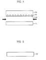
- FIGS. 2A through 5 illustrate a method for preparing a compound semiconductor substrate according to an exemplary embodiment
- FIG. 6 is a transmission electron microscope (TEM) image of a sample on which a spherical ball coating is performed twice;
- FIGS. 7A through 10 illustrate a method for preparing a compound semiconductor substrate according to another exemplary embodiment.
- Embodiments are mainly focused on a spherical ball treatment on a substrate.
- the spherical ball treatment is equally or more effective than typical mask patterning process in reducing dislocations.
- the spherical balls may generate voids between a substrate and a compound semiconductor epitaxial layer so that the substrate and the compound semiconductor epitaxial layer are self-separated along the voids.
- FIGS. 2A through 5 illustrate a method for preparing a compound semiconductor substrate according to an exemplary embodiment.
- FIGS. 2A and 3 through 5 are cross-sectional views and
- FIG. 2B is a plan view.
- a plurality of spherical balls 20 are coated on a substrate 10.
- the substrate 10 may be formed of sapphire, silicon carbide (SiC), silicon, or any other typical semiconductor material suitable for growing a compound semiconductor epitaxial layer.
- the substrate 10 may be formed of a gallium arsenide (GaAs) single crystal, a spinel single crystal, an indium phosphide (InP) single crystal, a silicon carbide (SiC) single crystal, or a gallium nitride (GaN) single crystal.
- a buffer layer of gallium nitride (GaN) may be formed on such single crystals. Because all the materials have both strengths and weaknesses, respectively, the material for the substrate can be appropriately selected according to the requirements. For example, when a large area is required, the substrate may be formed of silicon.
- the spherical balls 20 may be formed of a metal oxide, such as silica (SiO 2 ), sapphire (Al 2 O 3 ), zirconia (ZrO 2 ) and yttria-zirconia (Y 2 O 3 -ZrO 2 ).
- the spherical balls 20 may be formed of a material based on a stable oxide that does not react with the substrate 10 and a compound semiconductor epitaxial layer 30 even at a growth temperature of a compound semiconductor epitaxial layer, which will be described later.
- the spherical balls 20 may be formed of a variety of materials, and may also be obtained commercially.
- the spherical balls 20 may have a wide range of size from nanometers to tens of micrometers. In view of size and easiness of manufacturing and removing, the spherical balls are preferably formed of silica. A method for producing the silica balls is described in Korean Patent Application No. 2005-0019605, filed March 9, 2005 .
- the spherical balls 20 may be coated on the substrate 10 using a simple method such as dropping, dip coating and spin coating, after being dispersed in a suitable solvent. If necessary, drying may be performed to evaporate the solvent.
- the density of the spherical balls on the substrate 10 may be controlled using the loading density of the spherical balls in the solvent, the thickness of the coating, the number of coatings, and the like.
- the substrate 10 coated with the spherical balls 20 is placed in a furnace so that the compound semiconductor epitaxial layer 30 is grown on the substrate 10.
- the compound semiconductor epitaxial layer 30 is grown to a thickness greater than the size of the spherical balls 20. That is, the compound semiconductor epitaxial layer 30 is grown to cover the spherical balls 20 completely.
- the compound semiconductor epitaxial layer 30 is grown to a thickness adequate for the final compound semiconductor substrate.
- the compound semiconductor epitaxial layer 30 may be grown using metal-organic chemical vapor deposition (MOCVD), molecular beam epitaxy (MBE), or hydride vapor phase epitaxy (HVPE).
- MOCVD metal-organic chemical vapor deposition
- MBE molecular beam epitaxy
- HVPE hydride vapor phase epitaxy
- the compound semiconductor epitaxial layer 30 may be formed of gallium nitride (GaN), aluminum nitride (AlN), indium nitride (InN), or a combination (Ga 1-x Al 1-y In 1-z N, where 0 ⁇ x, y, z ⁇ 1) thereof.
- the compound semiconductor epitaxial layer 30 may be formed of a gallium nitride alloy such as aluminum gallium nitride (AlGaN), indium gallium nitride (InGaN) and aluminum indium gallium nitride (AlInGaN).
- AlGaN aluminum gallium nitride
- InGaN indium gallium nitride
- AlInGaN aluminum indium gallium nitride
- a metal organic (MO) source including gallium (Ga), such as trimethyl gallium (TMGa), triethyl gallium (TEGa) and gallium chloride (GaCl 3 ), and a nitrogen-containing gas, such as nitrogen (N 2 ), ammonia (NH 3 ) and tertiary butyl amine (N(C 4 H 9 )H 2 ) may be applied to the surface of the substrate 10.
- MO metal organic
- Ga gallium
- TMGa trimethyl gallium
- TMGa triethyl gallium
- GaCl 3 gallium chloride
- N 2 nitrogen
- NH 3 ammonia
- N(C 4 H 9 )H 2 tertiary butyl amine
- the gallium melt is reacted with hydrogen chloride (HCl) to produce gallium chloride (GaCl) gas.
- the gallium chloride (GaCl) gas is reacted with ammonia (NH 3 ) to form gallium nitride.
- the spherical balls 20 function as the typical mask pattern because they do not cover the whole surface of the substrate 10. That is, nucleation and growth of portions of the compound semiconductor epitaxial layer 30 begin to occur on the exposed upper surface of the substrate 10. Thereafter, due to the epitaxial lateral overgrowth (ELO), the lateral growth fronts coalesce with each other over the spherical balls 20, and then, the compound semiconductor epitaxial layer 30 further extends upwardly. As a result, because of the spherical balls 20, dislocations are bent to thereby improve optical properties and crystallographic properties of the compound semiconductor epitaxial layer 30. In addition, voids 35 are formed under the spherical balls 20.
- ELO epitaxial lateral overgrowth
- the compound semiconductor epitaxial layer 30 is grown at a high temperature of approximately 1,000 °C.
- the substrate 10 is inevitably cooled down to a lower temperature, e.g. to a room temperature.
- stress is concentrated at the voids to form brittle interfaces.
- the substrate 10 and the compound semiconductor epitaxial layer 30 can be easily separated along the voids 35. Even though they are not completely separated just after the cooling, they are in a state to be easily separated by only a very small mechanical force, e.g., by a worker.
- an additional laser lift-off process is not required.
- the spherical balls 20 may be separated not only from the compound semiconductor epitaxial layer 30 but also from the substrate 10. However, it is also possible that some of the spherical balls 20 remain on the substrate 10 and the others remain on the compound semiconductor epitaxial layer 30. In addition, it is also possible that all the spherical balls 20 remain on the compound semiconductor epitaxial layer 30. Therefore, in the case where the compound semiconductor epitaxial layer 30 itself is used as a compound semiconductor substrate, there may be a need for removing the spherical balls 20 remaining on the compound semiconductor epitaxial layer 30.
- the spherical balls 30 can be easily separated or removed using a mechanical method such as ultrasonic cleaning and megasonic cleaning, or a chemical etching because they are not strongly adhere thereto. Specifically, if the spherical balls are made of silica, they can be chemically etched out easily by immersing the compound semiconductor epitaxial layer 30 in a diluent of HF. The surface of the compound semiconductor epitaxial layer 30 is uneven after removing the spherical balls 20. Accordingly, an appropriate polishing may be performed to prepare the final compound semiconductor substrate 30' as shown in FIG. 5 .
- a gallium nitride substrate can be obtained when gallium nitride is grown as the compound semiconductor epitaxial layer 30, and an aluminum nitride substrate can be obtained when aluminum nitride is grown as the compound semiconductor epitaxial layer 30.
- the simple spherical ball treatment can reduce the process time and the process cost as compared to the typical mask patterning process. At the same time, the simple spherical ball treatment can reduce internal generation of linear dislocations during the gallium nitride growth. Furthermore, the separate process for separating the gallium nitride from the substrate can be omitted.
- the sequential processes of coating the spherical balls 20 and growing the compound semiconductor epitaxial layer 30 may be performed repeatedly to improve the quality of the compound semiconductor epitaxial layer 30. That is, the coating of the spherical balls 20 and the growing of the compound semiconductor epitaxial layer 30 may be performed once more on the compound semiconductor epitaxial layer 30 of FIG. 3 .
- the multiple layers of the spherical balls 20 can make the dislocations be bent primarily and secondarily in the compound semiconductor epitaxial layer 30.
- FIG. 6 is a transmission electron microscope (TEM) image of a sample on which the spherical ball coating is performed twice. That is, the sample is obtained by coating silica balls 20a on a sapphire substrate 10a, growing a gallium nitride epitaxial layer 30a, coating the silica balls 20a again on the gallium nitride epitaxial layer 30a, and then growing the gallium nitride layer 30a further.
- TEM transmission electron microscope
- voids 35a are formed under the silica balls 20a.
- dislocations 40 are bent by the spherical balls 20a, and the sapphire substrate 10a and the gallium nitride epitaxial layer 30a are in a state to be easily separated along the voids 35a.
- FIGS. 7A through 10 illustrate a method for preparing a compound semiconductor substrate according to another exemplary embodiment.
- FIGS. 7A , 8A , 9 and 10 are cross-sectional views
- FIGS. 7B and 8B are scanning electron microscope (SEM) images of upper surfaces of FIGS. 7A and 8A , respectively.
- a plurality of spherical balls are coated on a substrate 10.
- the substrate 10 is placed in a furnace so that a first compound semiconductor epitaxial layer 50 is grown on the substrate 10.
- the first compound semiconductor epitaxial layer 50 is grown to a thickness smaller than the size of the spherical balls 20. That is, the first compound semiconductor epitaxial layer 50 does not completely cover the spherical balls 20 to remove the spherical balls 20 in a subsequent process.
- the first compound semiconductor epitaxial layer 50 is formed of a chemically stable material, i.e., a material having a crystallographic property identical to or similar to that of a material for a second compound semiconductor epitaxial layer 60 which will be grown in a subsequent process.
- a chemically stable material i.e., a material having a crystallographic property identical to or similar to that of a material for a second compound semiconductor epitaxial layer 60 which will be grown in a subsequent process.
- crystallographic difference and thus a density of crystal defects can be minimized between the first compound semiconductor epitaxial layer 50 and the second compound semiconductor epitaxial layer 60.
- the first compound semiconductor epitaxial layer 50 is formed of a material having a lattice constant and a thermal expansion coefficient identical to or similar to those of a material for the second compound semiconductor epitaxial layer 60, so that the first compound semiconductor epitaxial layer 50 functions as a buffer layer.
- the first compound semiconductor epitaxial layer 50 may be grown using MOCVD, MBE, HVPE, or the like.
- the first compound semiconductor epitaxial layer 50 may be formed of gallium nitride (GaN), aluminum nitride (AlN), indium nitride (InN), or a combination (Ga 1-x Al 1-y In 1-z N, where 0 ⁇ x, y, z ⁇ 1) thereof.
- the spherical balls 20 are removed from the substrate 10.
- the spherical balls 20 can be easily removed using ultrasonic cleaning, megasonic cleaning, or chemical etching.
- nearly spherical voids 55 are formed where the spherical balls 20 are removed, to expose a portion of the upper surface of the substrate 10.
- the first compound semiconductor epitaxial layer 50 with the voids 55 remains on the substrate 10.
- the second compound semiconductor epitaxial layer 60 is grown on the first compound semiconductor epitaxial layer 50.
- the second compound semiconductor epitaxial layer 60 may also be grown using MOCVD, MBE, HVPE, or the like.
- the second compound semiconductor epitaxial layer 60 may be formed of gallium nitride (GaN), aluminum nitride (AlN), indium nitride (InN), or a combination (Ga 1-x Al 1-y In 1-z N, where 0 ⁇ x, y, z ⁇ 1) thereof.
- the second compound semiconductor epitaxial layer 60 has a suitable thickness to function as a final compound semiconductor substrate.
- the second compound semiconductor epitaxial layer 60 grows on the first compound semiconductor epitaxial layer 50 to a desired thickness, and at the same time, the lateral growth fronts coalesce with each other. Resultantly, the continuous second compound semiconductor epitaxial layer 60 is formed on the first compound semiconductor epitaxial layer 50 with a plurality of vacancies, i.e., the plurality of voids 55, therein.
- the growth temperature of the second compound semiconductor epitaxial layer 60 is approximately 1,000 °C.
- the substrate 10 is inevitably cooled down to a lower temperature. During the cooling, stress is concentrated at the voids 55 to form brittle interfaces. Consequently, as shown in FIG. 10 , the second compound semiconductor epitaxial layer 60 can be separated from the substrate 10 and the first compound semiconductor epitaxial layer 50 along the voids 55. Even though it is not completely separated just after the cooling, it is in a state to be easily separated by only a very small mechanical force. As described above, by separating the second compound semiconductor epitaxial layer 60 through the self-separation, the compound semiconductor substrate can be obtained.
- the spherical balls are coated on the substrate, and the compound semiconductor epitaxial layer is grown thereon.
- the spherical balls reduce the dislocation generations, increasing the quality of the grown compound semiconductor epitaxial layer.
- the voids under the spherical balls permit self-separation of the semiconductor epitaxial layer from the substrate. Accordingly, the compound semiconductor substrate of good quality can be prepared without the need of additional separation process such as laser lift-off. As a result, it is possible to reduce the process time and the process cost, and increase the process yield through the simple process, compared to the related art.
Landscapes
- Crystals, And After-Treatments Of Crystals (AREA)
- Liquid Deposition Of Substances Of Which Semiconductor Devices Are Composed (AREA)
- Chemical Vapour Deposition (AREA)
Priority Applications (1)
| Application Number | Priority Date | Filing Date | Title |
|---|---|---|---|
| EP11002687.9A EP2333817B1 (de) | 2007-10-24 | 2008-07-18 | Verfahren zur Herstellung eines Verbindungshalbleitersubstrats |
Applications Claiming Priority (1)
| Application Number | Priority Date | Filing Date | Title |
|---|---|---|---|
| KR1020070107090A KR100921789B1 (ko) | 2007-10-24 | 2007-10-24 | 화합물 반도체 기판 제조 방법 |
Related Child Applications (1)
| Application Number | Title | Priority Date | Filing Date |
|---|---|---|---|
| EP11002687.9A Division EP2333817B1 (de) | 2007-10-24 | 2008-07-18 | Verfahren zur Herstellung eines Verbindungshalbleitersubstrats |
Publications (2)
| Publication Number | Publication Date |
|---|---|
| EP2053637A2 true EP2053637A2 (de) | 2009-04-29 |
| EP2053637A3 EP2053637A3 (de) | 2010-04-28 |
Family
ID=40130585
Family Applications (2)
| Application Number | Title | Priority Date | Filing Date |
|---|---|---|---|
| EP08013037A Withdrawn EP2053637A3 (de) | 2007-10-24 | 2008-07-18 | Verfahren zur Herstellung eines Verbindungshalbleitersubstrats |
| EP11002687.9A Active EP2333817B1 (de) | 2007-10-24 | 2008-07-18 | Verfahren zur Herstellung eines Verbindungshalbleitersubstrats |
Family Applications After (1)
| Application Number | Title | Priority Date | Filing Date |
|---|---|---|---|
| EP11002687.9A Active EP2333817B1 (de) | 2007-10-24 | 2008-07-18 | Verfahren zur Herstellung eines Verbindungshalbleitersubstrats |
Country Status (6)
| Country | Link |
|---|---|
| US (2) | US7816241B2 (de) |
| EP (2) | EP2053637A3 (de) |
| JP (1) | JP2009102218A (de) |
| KR (1) | KR100921789B1 (de) |
| CN (1) | CN101436531B (de) |
| TW (1) | TWI442454B (de) |
Families Citing this family (12)
| Publication number | Priority date | Publication date | Assignee | Title |
|---|---|---|---|---|
| US7776152B2 (en) * | 2006-11-01 | 2010-08-17 | Raytheon Company | Method for continuous, in situ evaluation of entire wafers for macroscopic features during epitaxial growth |
| KR101101780B1 (ko) * | 2008-09-08 | 2012-01-05 | 서울대학교산학협력단 | 질화물 박막 구조 및 그 형성 방법 |
| US8680510B2 (en) | 2010-06-28 | 2014-03-25 | International Business Machines Corporation | Method of forming compound semiconductor |
| CN102719888B (zh) * | 2011-03-29 | 2015-11-25 | 清华大学 | 具有纳米微结构基板的制备方法 |
| US20150087137A1 (en) * | 2011-03-07 | 2015-03-26 | Snu R&Db Foundation | Nitride thin film stucture and method of forming the same |
| CN102817074B (zh) * | 2012-07-23 | 2015-09-30 | 北京燕园中镓半导体工程研发中心有限公司 | 基于原位应力控制的iii族氮化物厚膜自分离方法 |
| JP5997373B2 (ja) * | 2013-08-21 | 2016-09-28 | シャープ株式会社 | 窒化物半導体発光素子 |
| KR102099877B1 (ko) | 2013-11-05 | 2020-04-10 | 삼성전자 주식회사 | 질화물 반도체 디바이스의 제조 방법 |
| JP6465114B2 (ja) * | 2014-08-12 | 2019-02-06 | Tdk株式会社 | アルミナ基板 |
| KR101636140B1 (ko) * | 2014-08-22 | 2016-07-07 | 한양대학교 산학협력단 | 발광 소자 및 그 제조 방법 |
| JP6503819B2 (ja) * | 2015-03-23 | 2019-04-24 | Tdk株式会社 | アルミナ基板 |
| CN114639593A (zh) * | 2022-01-26 | 2022-06-17 | 西安电子科技大学 | 基于二氧化硅微纳球的氮化物异质外延材料及制备方法 |
Citations (3)
| Publication number | Priority date | Publication date | Assignee | Title |
|---|---|---|---|---|
| KR20040078208A (ko) | 2003-03-03 | 2004-09-10 | 엘지전자 주식회사 | 질화갈륨 기판 제조 방법 |
| KR20050019605A (ko) | 2003-08-20 | 2005-03-03 | 주식회사 닥터골드 | 귀금속 판매 관리 방법 |
| KR20070107090A (ko) | 2005-03-02 | 2007-11-06 | 오토리브 디벨로프먼트 에이비 | 관형 가스 안내 부재, 가스 생성 및 주입 유니트 및 에어백유니트 |
Family Cites Families (15)
| Publication number | Priority date | Publication date | Assignee | Title |
|---|---|---|---|---|
| US6657232B2 (en) * | 2000-04-17 | 2003-12-02 | Virginia Commonwealth University | Defect reduction in GaN and related materials |
| JP3631724B2 (ja) * | 2001-03-27 | 2005-03-23 | 日本電気株式会社 | Iii族窒化物半導体基板およびその製造方法 |
| KR20050029735A (ko) * | 2003-09-22 | 2005-03-28 | 엘지전자 주식회사 | 결함을 줄이고 분리가 용이한 질화갈륨 후막 성장 방법 |
| US7253104B2 (en) * | 2003-12-01 | 2007-08-07 | Micron Technology, Inc. | Methods of forming particle-containing materials |
| KR100682880B1 (ko) * | 2005-01-07 | 2007-02-15 | 삼성코닝 주식회사 | 결정 성장 방법 |
| KR100712753B1 (ko) * | 2005-03-09 | 2007-04-30 | 주식회사 실트론 | 화합물 반도체 장치 및 그 제조방법 |
| JP2006352079A (ja) * | 2005-03-22 | 2006-12-28 | Sumitomo Chemical Co Ltd | 自立基板、その製造方法及び半導体発光素子 |
| JP2007001855A (ja) * | 2005-05-27 | 2007-01-11 | Sumitomo Chemical Co Ltd | 3−5族窒化物半導体積層基板、3−5族窒化物半導体自立基板の製造方法、及び半導体素子 |
| JP2007019318A (ja) * | 2005-07-08 | 2007-01-25 | Sumitomo Chemical Co Ltd | 半導体発光素子、半導体発光素子用基板の製造方法及び半導体発光素子の製造方法 |
| US8691674B2 (en) * | 2005-09-29 | 2014-04-08 | Sumitomo Chemical Company, Limited | Method for producing group 3-5 nitride semiconductor and method for producing light-emitting device |
| CN100585885C (zh) * | 2006-01-27 | 2010-01-27 | 杭州士兰明芯科技有限公司 | 蓝宝石衬底粗糙化的发光二极管及其制造方法 |
| JP4879614B2 (ja) * | 2006-03-13 | 2012-02-22 | 住友化学株式会社 | 3−5族窒化物半導体基板の製造方法 |
| KR100831843B1 (ko) * | 2006-11-07 | 2008-05-22 | 주식회사 실트론 | 금속층 위에 성장된 화합물 반도체 기판, 그 제조 방법 및이를 이용한 화합물 반도체 소자 |
| US7560747B2 (en) * | 2007-05-01 | 2009-07-14 | Eastman Kodak Company | Light-emitting device having improved light output |
| TWI338387B (en) * | 2007-05-28 | 2011-03-01 | Delta Electronics Inc | Current spreading layer with micro/nano structure, light-emitting diode apparatus and its manufacturing method |
-
2007
- 2007-10-24 KR KR1020070107090A patent/KR100921789B1/ko active Active
-
2008
- 2008-07-18 EP EP08013037A patent/EP2053637A3/de not_active Withdrawn
- 2008-07-18 EP EP11002687.9A patent/EP2333817B1/de active Active
- 2008-07-23 US US12/177,917 patent/US7816241B2/en active Active
- 2008-07-24 JP JP2008190934A patent/JP2009102218A/ja active Pending
- 2008-09-26 CN CN2008102114942A patent/CN101436531B/zh not_active Expired - Fee Related
- 2008-10-07 TW TW097138559A patent/TWI442454B/zh active
-
2010
- 2010-09-09 US US12/878,225 patent/US8158496B2/en active Active
Patent Citations (3)
| Publication number | Priority date | Publication date | Assignee | Title |
|---|---|---|---|---|
| KR20040078208A (ko) | 2003-03-03 | 2004-09-10 | 엘지전자 주식회사 | 질화갈륨 기판 제조 방법 |
| KR20050019605A (ko) | 2003-08-20 | 2005-03-03 | 주식회사 닥터골드 | 귀금속 판매 관리 방법 |
| KR20070107090A (ko) | 2005-03-02 | 2007-11-06 | 오토리브 디벨로프먼트 에이비 | 관형 가스 안내 부재, 가스 생성 및 주입 유니트 및 에어백유니트 |
Also Published As
| Publication number | Publication date |
|---|---|
| KR100921789B1 (ko) | 2009-10-15 |
| US20100330784A1 (en) | 2010-12-30 |
| US7816241B2 (en) | 2010-10-19 |
| EP2333817A2 (de) | 2011-06-15 |
| US20090111250A1 (en) | 2009-04-30 |
| US8158496B2 (en) | 2012-04-17 |
| KR20090041536A (ko) | 2009-04-29 |
| EP2333817A3 (de) | 2012-05-23 |
| EP2333817B1 (de) | 2015-04-15 |
| TW200919551A (en) | 2009-05-01 |
| EP2053637A3 (de) | 2010-04-28 |
| JP2009102218A (ja) | 2009-05-14 |
| TWI442454B (zh) | 2014-06-21 |
| CN101436531A (zh) | 2009-05-20 |
| CN101436531B (zh) | 2012-07-04 |
Similar Documents
| Publication | Publication Date | Title |
|---|---|---|
| US8158496B2 (en) | Method for preparing compound semiconductor substrate | |
| US7708832B2 (en) | Method for preparing substrate for growing gallium nitride and method for preparing gallium nitride substrate | |
| JP4581490B2 (ja) | Iii−v族窒化物系半導体自立基板の製造方法、及びiii−v族窒化物系半導体の製造方法 | |
| KR100682880B1 (ko) | 결정 성장 방법 | |
| JP4932121B2 (ja) | Iii−v族窒化物系半導体基板の製造方法 | |
| JP4735949B2 (ja) | Iii−v族窒化物半導体結晶の製造方法およびiii−v族窒化物半導体基板の製造方法 | |
| CN100418191C (zh) | 外延生长方法 | |
| US7723217B2 (en) | Method for manufacturing gallium nitride single crystalline substrate using self-split | |
| US20070092980A1 (en) | Method of fabricating GaN | |
| US20060160334A1 (en) | Epitaxial growth method | |
| US20220199395A1 (en) | Optimizing growth method for improving quality of mocvd epitaxial thin films | |
| JP2011216549A (ja) | GaN系半導体エピタキシャル基板の製造方法 | |
| KR20160136581A (ko) | 벽개 특성을 이용한 질화물 반도체 기판 제조 방법 | |
| WO2010116596A1 (ja) | Iii族窒化物半導体自立基板の製造方法及びiii族窒化物半導体層成長用基板 | |
| KR20090044707A (ko) | 화합물 반도체 기판 제조방법 |
Legal Events
| Date | Code | Title | Description |
|---|---|---|---|
| PUAI | Public reference made under article 153(3) epc to a published international application that has entered the european phase |
Free format text: ORIGINAL CODE: 0009012 |
|
| AK | Designated contracting states |
Kind code of ref document: A2 Designated state(s): AT BE BG CH CY CZ DE DK EE ES FI FR GB GR HR HU IE IS IT LI LT LU LV MC MT NL NO PL PT RO SE SI SK TR |
|
| AX | Request for extension of the european patent |
Extension state: AL BA MK RS |
|
| PUAL | Search report despatched |
Free format text: ORIGINAL CODE: 0009013 |
|
| AK | Designated contracting states |
Kind code of ref document: A3 Designated state(s): AT BE BG CH CY CZ DE DK EE ES FI FR GB GR HR HU IE IS IT LI LT LU LV MC MT NL NO PL PT RO SE SI SK TR |
|
| AX | Request for extension of the european patent |
Extension state: AL BA MK RS |
|
| RIC1 | Information provided on ipc code assigned before grant |
Ipc: H01L 21/02 20060101ALI20100322BHEP Ipc: H01L 21/20 20060101AFI20090107BHEP |
|
| 17P | Request for examination filed |
Effective date: 20101028 |
|
| 17Q | First examination report despatched |
Effective date: 20101123 |
|
| AKX | Designation fees paid |
Designated state(s): DE FR NL |
|
| STAA | Information on the status of an ep patent application or granted ep patent |
Free format text: STATUS: THE APPLICATION IS DEEMED TO BE WITHDRAWN |
|
| 18D | Application deemed to be withdrawn |
Effective date: 20121024 |