EP2053731B1 - Stromwandlereinrichtung und steuerverfahren für die einrichtung - Google Patents
Stromwandlereinrichtung und steuerverfahren für die einrichtung Download PDFInfo
- Publication number
- EP2053731B1 EP2053731B1 EP07741773.1A EP07741773A EP2053731B1 EP 2053731 B1 EP2053731 B1 EP 2053731B1 EP 07741773 A EP07741773 A EP 07741773A EP 2053731 B1 EP2053731 B1 EP 2053731B1
- Authority
- EP
- European Patent Office
- Prior art keywords
- phase
- voltage
- instruction signal
- section
- generating part
- Prior art date
- Legal status (The legal status is an assumption and is not a legal conclusion. Google has not performed a legal analysis and makes no representation as to the accuracy of the status listed.)
- Active
Links
Images





Classifications
-
- H—ELECTRICITY
- H02—GENERATION; CONVERSION OR DISTRIBUTION OF ELECTRIC POWER
- H02M—APPARATUS FOR CONVERSION BETWEEN AC AND AC, BETWEEN AC AND DC, OR BETWEEN DC AND DC, AND FOR USE WITH MAINS OR SIMILAR POWER SUPPLY SYSTEMS; CONVERSION OF DC OR AC INPUT POWER INTO SURGE OUTPUT POWER; CONTROL OR REGULATION THEREOF
- H02M7/00—Conversion of AC power input into DC power output; Conversion of DC power input into AC power output
- H02M7/42—Conversion of DC power input into AC power output without possibility of reversal
- H02M7/44—Conversion of DC power input into AC power output without possibility of reversal by static converters
- H02M7/48—Conversion of DC power input into AC power output without possibility of reversal by static converters using discharge tubes with control electrode or semiconductor devices with control electrode
- H02M7/53—Conversion of DC power input into AC power output without possibility of reversal by static converters using discharge tubes with control electrode or semiconductor devices with control electrode using devices of a triode or transistor type requiring continuous application of a control signal
- H02M7/537—Conversion of DC power input into AC power output without possibility of reversal by static converters using discharge tubes with control electrode or semiconductor devices with control electrode using devices of a triode or transistor type requiring continuous application of a control signal using semiconductor devices only, e.g. single switched pulse inverters
- H02M7/5387—Conversion of DC power input into AC power output without possibility of reversal by static converters using discharge tubes with control electrode or semiconductor devices with control electrode using devices of a triode or transistor type requiring continuous application of a control signal using semiconductor devices only, e.g. single switched pulse inverters in a bridge configuration
- H02M7/53871—Conversion of DC power input into AC power output without possibility of reversal by static converters using discharge tubes with control electrode or semiconductor devices with control electrode using devices of a triode or transistor type requiring continuous application of a control signal using semiconductor devices only, e.g. single switched pulse inverters in a bridge configuration with automatic control of output voltage or current
- H02M7/53875—Conversion of DC power input into AC power output without possibility of reversal by static converters using discharge tubes with control electrode or semiconductor devices with control electrode using devices of a triode or transistor type requiring continuous application of a control signal using semiconductor devices only, e.g. single switched pulse inverters in a bridge configuration with automatic control of output voltage or current with analogue control of three-phase output
-
- H—ELECTRICITY
- H02—GENERATION; CONVERSION OR DISTRIBUTION OF ELECTRIC POWER
- H02M—APPARATUS FOR CONVERSION BETWEEN AC AND AC, BETWEEN AC AND DC, OR BETWEEN DC AND DC, AND FOR USE WITH MAINS OR SIMILAR POWER SUPPLY SYSTEMS; CONVERSION OF DC OR AC INPUT POWER INTO SURGE OUTPUT POWER; CONTROL OR REGULATION THEREOF
- H02M7/00—Conversion of AC power input into DC power output; Conversion of DC power input into AC power output
- H02M7/42—Conversion of DC power input into AC power output without possibility of reversal
- H02M7/44—Conversion of DC power input into AC power output without possibility of reversal by static converters
- H02M7/48—Conversion of DC power input into AC power output without possibility of reversal by static converters using discharge tubes with control electrode or semiconductor devices with control electrode
-
- H—ELECTRICITY
- H02—GENERATION; CONVERSION OR DISTRIBUTION OF ELECTRIC POWER
- H02M—APPARATUS FOR CONVERSION BETWEEN AC AND AC, BETWEEN AC AND DC, OR BETWEEN DC AND DC, AND FOR USE WITH MAINS OR SIMILAR POWER SUPPLY SYSTEMS; CONVERSION OF DC OR AC INPUT POWER INTO SURGE OUTPUT POWER; CONTROL OR REGULATION THEREOF
- H02M7/00—Conversion of AC power input into DC power output; Conversion of DC power input into AC power output
- H02M7/02—Conversion of AC power input into DC power output without possibility of reversal
- H02M7/04—Conversion of AC power input into DC power output without possibility of reversal by static converters
- H02M7/12—Conversion of AC power input into DC power output without possibility of reversal by static converters using discharge tubes with control electrode or semiconductor devices with control electrode
Definitions
- the present invention relates to a power converter apparatus and a power converter apparatus control method.
- an indirect ac power converter circuit that converts a commercial alternating current into a direct current via a rectifying circuit and a smoothing circuit and outputs a desired alternating current by a voltage type converter is generally used.
- a direct power converter apparatus represented by a matrix converter is known, and this obviates the need for a large-size capacitor or reactor for smoothing the voltage pulsation due to the commercial frequency. Therefore, downsizing of the converter can be expected, and the converter has attracted attention in recent years as a next-generation power converter apparatus.
- a direct power converter apparatus having a PWM rectifier that converts a three-phase ac voltage into a dc voltage and a PWM inverter that converts the dc voltage converted by the PWM rectifier into a prescribed three-phase ac output voltage (refer to, for example, JP 2004-266972 A ).
- the direct power converter apparatus generates a trapezoidal waveform instruction signal on the basis of an input current instruction and compares the trapezoidal waveform instruction signal with a carrier signal to generate a PWM modulation signal for turning on and off the switching circuit of the PWM rectifier. Moreover, the direct power converter apparatus compares a triangular wave obtained by transforming the carrier signal with an output voltage instruction to generate a PWM modulation signal for turning on and off the switching circuit of the PWM inverter.
- the direct power converter apparatus generates the trapezoidal waveform instruction signal by calculation on the basis of an input current instruction, the direct power converter apparatus has a problem that the operational load of the control section increases.
- the direct power converter apparatus needs to transform the carrier waveform on the PWM inverter side, the direct power converter apparatus has a problem that the modulation waveform generation is complicated, and the control circuit becomes complicated. There is a further problem that the circuit of the control section becomes complicated also when a carrier generator circuit to supply a carrier signal is separately used for the PWM rectifier and the PWM inverter.
- control apparatus detects first phase signals fixed in relative phase to induced voltages of the motor and current polarity signals, recognizes phase differences between them, generates second phase signals so as to make the phase differences approach zero to drive the motor at high-efficiency, generates modulation based signals having quasi-sinusoidal waveform or trapezoidal waveform on the basis of the second phase signals, compares the modulation wave signals with a carrier wave signal, and conducts PWM control on an inverter.
- An object of the invention is to provide a power converter apparatus and a power converter apparatus control method capable of reducing the operational load of the control section with a simple construction.
- Another object of the invention is to provide a power converter apparatus and a power converter apparatus control method capable of simplifying the circuit of the control section.
- a power converter apparatus of a first aspect of the invention comprises, in particular:
- the signal that becomes the reference of the three-phase ac input voltages is used when the converting section converts the three-phase ac input voltage into the dc voltage
- the signal that becomes the reference for producing, for example, the three-phase ac output voltage is used when the converting section converts the dc voltage into the three-phase ac output voltage.
- the trapezoidal waveform instruction signal needs not be formed by complicated calculation, and the operational load of the control section can be reduced with a simple construction.
- a power converter apparatus of a second aspect of the invention comprises, in particular: a power converter apparatus, which has a converter section that converts a three-phase ac input voltage into a dc voltage and an inverter section that converts the dc voltage converted by the converter section into a prescribed three-phase ac output voltage and which has no smoothing filter in a dc link portion that connects the converter section with the inverter section, the apparatus comprising:
- the dc voltage converted by the converter section can be converted into the prescribed three-phase ac output voltage on the basis of the corrected inverter section instruction signal.
- the converter section instruction signal of the trapezoidal waveform needs not be formed by complicated calculation, and the operational load of the control section can be reduced with a simple construction.
- the prescribed equations are: 3 tan ⁇ ⁇ ⁇ / 6 (provided that the phase angle ⁇ is 0 ⁇ ⁇ ⁇ ⁇ /3) and ⁇ 3 tan ⁇ ⁇ ⁇ / 6 (provided that the phase angle ⁇ is ⁇ ⁇ ⁇ ⁇ 4 ⁇ /3).
- the converter section instruction signal of the trapezoidal waveform by the converter section instruction signal generating part using the prescribed equation, the three-phase ac output voltage (current) free of distortion can reliably be obtained while reducing the operational load.
- the circuit of the control section can be simplified by enabling the PWM modulation by one carrier signal common to the converter section and the inverter section.
- the carrier signal is a signal of a triangular waveform.
- the circuit for the pulse width modulation can be simplified by using the signal of the triangular waveform suitable for the PWM modulation for the carrier signal.
- the carrier signal is a signal of a sawtooth waveform.
- the carrier generation and the modulation processing can be simplified by using the signal of the sawtooth waveform for the carrier signal.
- the converter section comprises:
- An embodiment is a matrix converter having a virtual converter section corresponding to the converter section, a virtual inverter section corresponding to the inverter section, and a virtual dc link portion corresponding to the dc link portion, wherein the virtual converter section and the virtual inverter section comprises:
- the signal that becomes the reference of the three-phase ac input voltages is used when the converting section converts the three-phase ac input voltage into the dc voltage
- the signal that becomes the reference for producing, for example, the three-phase ac output voltage is used when the converting section converts the dc voltage into the three-phase ac output voltage.
- the dc voltage converted by the converter section can be converted into the prescribed three-phase ac output voltage on the basis of the corrected inverter section instruction signal.
- the converter section comprises:
- a power converter apparatus of a third aspect of the invention comprises:
- the circuit of the control section can be simplified by enabling the PWM modulation by one carrier signal common to the converter section and the inverter section.
- the carrier signal is a signal of a triangular waveform.
- the circuit for the pulse width modulation can be simplified by using the signal of the triangular waveform suitable for the PWM modulation for the carrier signal.
- the carrier signal is a signal of a sawtooth waveform.
- the carrier generation and the modulation processing can be simplified by using the signal of the sawtooth waveform for the carrier signal.
- a power converter apparatus control method comprising the steps of:
- the trapezoidal waveform instruction signal needs not be formed by complicated calculation, and the operational load of the control section can be reduced with a simple construction.
- a power converter apparatus control method for a power converter apparatus which has a converter section that converts a three-phase ac input voltage into a dc voltage and an inverter section that converts the dc voltage converted by the converter section into a prescribed three-phase ac output voltage and which has no smoothing filter in a dc link portion that connects the converter section with the inverter section, the method comprising the steps of:
- the dc voltage converted by the converter section can be converted into the prescribed three-phase ac output voltage on the basis of the corrected inverter section instruction signal.
- the converter section instruction signal of the trapezoidal waveform needs not be formed by complicated calculation, and the operational load of the control section can be reduced with a simple construction.
- the prescribed equations are: 3 tan ⁇ ⁇ ⁇ / 6 (provided that the phase angle ⁇ is 0 ⁇ ⁇ ⁇ ⁇ /3) and ⁇ 3 tan ⁇ ⁇ ⁇ / 6 (provided that the phase angle ⁇ is ⁇ ⁇ ⁇ ⁇ 4 ⁇ /3).
- the converter section instruction signal of the trapezoidal waveform by the converter section instruction signal generating part using the prescribed equation, the three-phase ac output voltage (current) free of distortion can reliably be obtained while reducing the operational load.
- the dc voltage converted by the converter section can be converted into the prescribed three-phase ac output voltage on the basis of the corrected inverter section instruction signal.
- a power converter apparatus control method comprising the steps of:
- the circuit of the control section can be simplified by enabling the PWM modulation by one carrier signal common to the converter section and the inverter section.
- a power converter apparatus comprising:
- the instruction signal needs not be formed by complicated calculation, and the operational load of the control section can be reduced with a simple construction.
- a power converter apparatus which has a converter section that converts a three-phase ac input voltage into a dc voltage and an inverter section that converts the dc voltage converted by the converter section into a prescribed three-phase ac output voltage and which has no smoothing filter in a dc link portion that connects the converter section with the inverter section, the apparatus comprising:
- the dc voltage converted by the converter section is converted into the prescribed three-phase ac output voltage on the basis of the inverter section instruction signal corrected by the instruction signal correcting part so that no distortion occurs in the three-phase ac output voltage (current) with respect to the pulsating voltage (current) waveform of the dc voltage converted by the converter section.
- the instruction signal needs not be formed by complicated calculation, and the operational load of the control section can be reduced with a simple construction.
- a power converter apparatus comprising:
- the instruction signal needs not be formed by complicated calculation, and the operational load of the control section can be reduced with a simple construction.
- a power converter apparatus which has a converter section that converts a three-phase ac input voltage into a dc voltage and an inverter section that converts the dc voltage converted by the converter section into a prescribed three-phase ac output voltage and which has no smoothing filter in a dc link portion that connects the converter section with the inverter section, the apparatus comprising:
- the dc voltage converted by the converter section is converted into the prescribed three-phase ac output voltage on the basis of the inverter section instruction signal corrected by the instruction signal correcting part so that no distortion occurs in the three-phase ac output voltage (current) with respect to the pulsating voltage (current) waveform of the dc voltage converted by the converter section.
- the instruction signal needs not be formed by complicated calculation, and the operational load of the control section can be reduced with a simple construction.
- the operational load of the control section can be reduced with a simple construction.
- the circuit of the control section can be simplified by enabling the PWM modulation by one carrier signal common to the converter section and the inverter section.
- phase voltage signal wave capable of obtaining a sine wave output also for a pulsating voltage waveform is described as in the method of generating a phase voltage waveform capable of obtaining a line voltage of a sine waveform with respect to a constant dc voltage.
- the Technical Document 1 is related to the modulation system of the direct conversion circuit with the dc link free of smoothing and rectifying circuits in the dc link portion.
- the direct conversion circuit with the dc link of the Technical Document 1 has a converter section constructed of six switching circuits S ap , S bp , S bp , S an , S bn , S cn that constitute a three-phase bridge circuit, and an inverter section constructed of six switching circuits S up , S vp , S wp , S un , S vn , S wn that constitute a three-phase bridge circuit.
- the converter section converts the three-phase ac input voltages V a , V b , V c from three-phase ac power sources V sa , V sb , V sc into direct currents.
- the inverter section converts a dc voltage V dc converted by the converter section into three-phase ac output voltages V su , V sv , V sw .
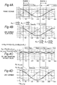
- Figs. 4A through 4D show the waveforms of parts based on the control principle of the direct conversion circuit with the dc link of the Technical Document 1.
- the phase voltages which correspond to either one of the two states of [two positive phases and one negative phase] and [two negative phases and one positive phase]
- the phase voltages can be divided into six regions every 60 degrees. In this case, a region 1 and a region 2 based on the c-phase are described.
- the c-phase of the minimum phase becomes conductive due to the switching circuit S cn
- the a-phase and b-phase of the maximum or intermediate phases are subjected to switching so as to have the following flow ratios d ac , d bc by using the switching circuits S ap , S bp
- the c-phase of the maximum phase becomes conductive due to the switching circuit S cp
- the a-phase and b-phase of the intermediate or minimum phases are subjected to switching so as to have the following flow ratios d ac , d bc by using the switching circuits S an , S bn .
- d ac cos ⁇ a cos ⁇ c
- d bc cos ⁇ b cos ⁇ c
- the flow ratios of the phases come to have the trapezoidal waveforms shown in Fig. 4B .
- the switching states of the upper arm and the lower arm on the converter side are shown. It is assumed that the upper arm becomes conductive when the flow ratio is positive and the lower arm becomes conductive when the flow ratio is negative.
- V dc 3 V m / 2 cos ⁇ in
- cos ⁇ in max cos ⁇ a cos ⁇ b cos ⁇ c by multiplying each dc link voltage by each flow ratio, and the dc link voltage comes to have a pulsating voltage waveform.
- the input currents respectively have a waveform obtained by multiplying the trapezoidal waveform flow ratio shown in Fig. 4B by the pulsating current, and therefore, are allowed to be the sine waves shown in Fig. 4D .
- the signals are shown based on the phase of the V uv line voltage as a reference in Technical
- V link max V uv V vw V wu
- Equation (7) the phase voltage instruction signals V u * *, V v **, V w ** are expressed by Equation (7) from the relation between the carrier amplitude and the output voltage of the following Equation (6) and is able to be further rewritten into Equation (8).
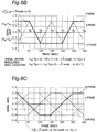
- Fig. 5A is the result of carrying out similar calculations for the six regions every phase angle of ⁇ /3, and a trapezoidal modulation waveform (phase voltage) of 120-degree electrification.
- the operational load of the control section can be reduced with a simple construction.
- the thus-obtained trapezoidal modulation waveform is equivalent to the line current instruction described in Technical Document 1. Since the line current of the current type corresponds to the line voltage of the voltage type, the line current instruction signals of Fig. 4B are compared with the trapezoidal modulation waveforms (line voltages) of Fig. 5C .
- the line voltage instruction signal generated by the power converter apparatus control method of the invention is equivalent to the line current instruction shown in Technical Document 1. Therefore, by applying, for example, the logical operation based on the duality (refer to Table 1 of Technical Document 3) of the voltage type and the current type shown in, for example, Technical Document 3 ( Takaharu Takeshita and two others, "PWM Scheme for Current Source Three-Phase Inverters and Converters", Trans. Inst. Elect. Engnr. Jpn. D, Vol.116, No.1, 1996 ), the current type PWM pattern can easily be generated from the voltage type.
- the method of generating the phase voltage instruction signal has been described above.
- the method can also be applied to a power converter apparatus of a spatial vector modulation system that uses a voltage vector besides the system with the triangular waveform carrier signal.
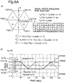
- Fig. 6A shows a vector diagram showing the spatial vectors of PWM modulation in the spatial vector modulation system and a chart showing the voltage vectors in Fig. 5A .
- V 1 - V 6 six states (V 1 - V 6 ) of eight states are vectors that are not zero, and the remaining two states (V 0 , V 7 ) are in the state of zero.
- FIG. 6A shows voltage vectors corresponding to the phase angle of 0 to ⁇ /3 in the line voltage control waveform of Fig. 5A .
- the voltage control factor ks is set to 0.5 in Fig. 6A .
- V st * 3 sin ⁇ ⁇ ⁇ / 6 / sin ⁇ + ⁇ / 3 + 1
- Fig. 7 shows the synchronous PWM modulation system described in JP 2004-266972 A by comparison to the modulation method of Technical Document 1.
- a carrier period t s a current instruction I(rt), a current instruction I(st), a flow ratio d rt , a flow ratio d st , input currents I r , I s , I t , a dc link current I dc , voltage instructions V 0 , V 4 , V 6 , a flow ratio d 0 corresponding to the voltage instruction V 0 , and a flow ratio d 4 corresponding to the voltage instruction V 4 .
- V u , V v , V w are the gate signals of the inverter.
- the carrier period on the converter side is divided into two switching states in which electrification of st, rt is effected. Further, since the flow ratios are varied, two carrier signals whose carrier amplitudes are varied every electrification period are used on the inverter side. Moreover, the signal wave to be compared with the carrier signal is corrected by the carrier amplitude by being multiplied by the flow ratio of the converter. Therefore, a complicated construction as described in JP 2004-266972 A results as a modulation circuit construction (description in the paragraphs [0021] through [0026] and Fig. 4 of JP 2004-266972 A ).
- FIG. 8 is a chart showing a PWM modulation system that uses a triangular waveform carrier signal of the power converter apparatus of the invention.
- a carrier period t s a current instruction I(rt), a current instruction I(st), a flow ratio d rt , a flow ratio d st , input currents I r , I s , I t , a dc link current I dc , voltage instructions V 0 , V 4 , V 6 , a flow ratio d 0 corresponding to the voltage instruction V 0 , and a flow ratio d 4 corresponding to the voltage instruction V 4 .
- V u , V v , V w are the gate signals of the upper arm
- /V u ', /V v ', /V w ' are the gate signals of the lower arm.
- an identical carrier signal is used on the converter side and the inverter side.
- one instruction signal is made to have an offset for comparison with the carrier signal, and the other instruction signal is inverted in polarity and compared with the carrier signal.
- a gate signal obtained by the operation is inverted.
- an inphase gate signal can be obtained by taking the logical sum of the gate signals in each period.
- Fig. 9 is a chart showing a PWM modulation system that uses a sawtooth waveform carrier signal of the power converter apparatus of the invention.
- a carrier period t s a current instruction I(rt), a current instruction I(st), a flow ratio d rt , a flow ratio d st , input currents I r , I s , I t , a dc link current I dc , voltage instructions V 0 , V 4 , V 6 , a flow ratio d 0 corresponding to the voltage instruction V 0 , a flow ratio d 4 corresponding to the voltage instruction V 4 , and a flow ratio d 6 corresponding to the voltage instruction V 6 .
- V u , V v , V w are the gate signals of the upper arm
- /V u ', /V v ', /V w ' are the gate signals of the lower arm.
- the power converter apparatus shown in Fig. 9 in which the carrier generation and modulation processing can be simplified, is suitable for software-oriented structure.
- the direct conversion circuit with the dc link described in Technical Document 1 needs to use the null vectors of both V 0 and V 7 to commutate the converter side in the null vector period, and this is disadvantageous in terms of three-phase modulation and loss on the inverter side.
- the frequency of the sawtooth wave becomes f with respect to the frequency 2f of the triangular wave of the principal component of the voltage spectrum due to the carrier, and it becomes inferior in terms of noise.
- the operational load in generating the instruction signals by the phase voltage instruction waveform on the carrier comparison basis (or the spatial vector modulation system) that causes no distortion in the line voltage (line current) with respect to the pulsating voltage (current) waveform can be reduced.
- the modulation circuit can be simplified.
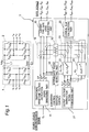
- Fig. 1 is a schematic diagram of the direct power converter apparatus with a dc link of the first embodiment of the invention.
- the direct power converter apparatus with a dc link of the first embodiment has no smoothing filter in the dc link portion that connects the converter section with the inverter section.
- the direct power converter apparatus has a converter section 1 constructed of switches S rp , S rn , S sp , S sn , S tp , S tn , an inverter section 2 constructed of switches S up , S un , S vp , S vn , S wp , S wn , and a control section 3 for outputting gate signals for turning on and off the switches S rp , S rn , S sp , S sn , S tp , S tn of the converter section 1 and the switches S up , S un , S vp , S vn , S wp , S wn of the inverter section 2.
- the switches S rp , S rn , S sp , S sn , S tp , S tn and the switches S up , S un , S vp , S vn , S wp , S wn are the switching circuits, which are each constituted by combining a plurality of switching elements.
- the phase voltage v r from a three-phase ac power source (not shown) is inputted to one terminal of the switch S rp and one terminal of the switch S rn , the phase voltage v s is inputted to one terminal of the switch S sp and one terminal of the switch S sn , and the phase voltage v t is inputted to one terminal of the switch S tp and one terminal of the switch S tn .
- the other terminal of the switches S rp , S sp , S tp is connected to a first dc link portion L1, while the other terminal of the switches S rn , S sn , S tn is connected to a second dc link portion L2.
- one terminal of the switch S up and one terminal of the switch S un are connected to the output terminal of the phase voltage v u of the three-phase ac output voltage
- one terminal of the switch S vp and one terminal of the switch S vn are connected to the output terminal of the phase voltage v v
- one terminal of the switch S wp and one terminal of the switch S wn are connected to the output terminal of the phase voltage v w .
- the other terminal of the switches S up , S vp , S wp is connected to the first dc link portion L1
- the other terminal of the switches S un , S vn , S wn is connected to the second dc link portion L2.
- the control section 3 has a trapezoidal waveform voltage instruction signal generating part 11 as one example of the instruction signal generating part for generating trapezoidal waveform voltage instruction signals V r *, V s *, V t * and the converter section instruction signal generating part on the basis of a power synchronization signal V r as one example of a reference signal for synchronization with the three-phase ac input voltage, a comparing part 12 for comparing the trapezoidal waveform voltage instruction signals V r *, V s *, V t * from the trapezoidal waveform voltage instruction signal generating part 11 with the carrier signal, a current type gate logic converting part 13 that outputs a gate signal on the basis of a comparison result from the comparing part 12, an intermediate phase detecting part 14 that detects flow ratios d rt , d st on the basis of the trapezoidal waveform voltage instruction signals V r *, V s *, V t * from the trapezoidal waveform voltage instruction signal generating part 11, a carrier signal generating
- the switches S rp , S rn , S sp , S sn , S tp , S tn of the converter section 1 are controlled to be turned on and off by the gate signal from the current type gate logic converting part 13, and the switches S up , S un , S vp , S vn , S wp , S wn of the inverter section 2 are controlled to be turned on and off by the gate signal from logical sum calculation part 25.
- the intermediate phase detecting part 14 and the calculation parts 22, 23 constitute an instruction signal correcting part.
- the comparing part 12 and the current type gate logic converting part 13 constitute a converter section PWM modulation signal generating part, while the comparing part 24 and the logical sum calculation part 25 constitute an inverter section PWM modulation signal generating part.
- the trapezoidal waveform voltage instruction signal generating part 11 generates sloped regions of the trapezoidal waveform voltage instruction signals V r *, V s *, V t * by using a prescribed table. In this case, as in Equation (8) described with reference to Figs.
- the phase angle ⁇ is synchronized with the phase voltage v r of the three-phase ac input voltage.
- the sloped regions of the trapezoidal waveform voltage instruction signals V r *, V s *, V t * may be obtained by using equations instead of the table.
- the output voltage instruction signals are corrected by the instruction signal correcting parts (14, 22, 23) so that no distortion occurs in the three-phase ac output voltage (current) with respect to the pulsating voltage (current) waveform of the dc voltage converted by the converter section 1.
- the dc voltage converted by the converter section 1 is converted into a prescribed three-phase ac output voltage on the basis of the corrected output voltage instruction signals.
- the trapezoidal waveform voltage instruction signal generating part 11 can reduce the operational load of the control section with a simple construction by generating the sloped regions of the trapezoidal waveform voltage instruction signals V r *, V s *, V t * by using the prescribed table (or the prescribed equation).
- the circuit of the control section can be simplified by enabling the PWM modulation by one carrier signal common to the converter section 1 and the inverter section 2.
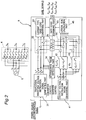
- Fig. 2 is a schematic diagram of a matrix converter as one example of the direct power converter apparatus of the second embodiment of the invention.
- the matrix converter has a converting section 4 constructed of switches S ur , S us , S ut , S vr , S vs , S vt , S wr , S ws , S wt , and a control section 5 that outputs gate signals for turning on and off the switches S ur , S us , S ut , S vr , S vs , S vt , S wr , S ws , Swt of the converting section 4.
- the converting section 4 corresponds to a virtual converter section and a virtual inverter section, and no smoothing filter is provided at a virtual dc link portion that connects the virtual converter section with the virtual inverter section.
- the switches S ur , S us , S ut , S vr , S vs , S vt , S wr , S ws , Swt are switching circuits constituted by combining a plurality of switching elements.
- the phase voltage v r of a three-phase ac input voltage from a three-phase ac power source 6 is inputted to one terminal of each of the switches S ur , S vr , S wr
- the phase voltage v s of the three-phase ac input voltage is inputted to one terminal of each of the switches S us , S vs , S ws
- the phase voltage v t of the three-phase ac input voltage is inputted to one terminal of each of the switches S ut , S vt , S wt .
- each of the switches S ur , S us , S ut is connected to the output terminal of the phase voltage v u
- the other terminal of each of the switches S vr , S vs , S vt is connected to the output terminal of the phase voltage v r
- the other terminal of each of the switches S wr , S ws , S wt is connected to the output terminal of the phase voltage v w .
- the control section 5 has a trapezoidal waveform voltage instruction signal generating part 31 as one example of the instruction signal generating part that generates trapezoidal waveform voltage instruction signals V r *, V s *, V t * and the converter section instruction signal generating part on the basis of a power synchronization signal V r as one example of the reference signal for synchronization with the three-phase ac input voltage, a comparing part 32 for comparing the trapezoidal waveform voltage instruction signals V r *, V s *, V t * from the trapezoidal waveform voltage instruction signal generating part 31 with a carrier signal, a current type gate logic converting part 33 that outputs a gate signal on the basis of a comparison result from the comparing part 32, an intermediate phase detecting part 34 that detects flow ratios d rt , d st on the basis of the trapezoidal waveform voltage instruction signals V r *, V s *, V t * from the trapezoidal waveform voltage instruction signal generating part 31, a carrier signal
- the switches S ur , S us , S ut , S vr , S vs , S vt , S wr , S ws , S wt of the converting section 4 are controlled to be turned on and off by the gate signals from the gate signal combining part 50.
- the intermediate phase detecting part 34 and the calculation parts 42, 43 constitute an instruction signal correcting part.
- the comparing part 32 and the current type gate logic converting part 33 constitute a converter section PWM modulation signal generating part, while the comparing part 44 and the logical sum calculation part 45 constitute an inverter section PWM modulation signal generating part.
- the trapezoidal waveform voltage instruction signal generating part 31 generates sloped regions of the trapezoidal waveform voltage instruction signals V r *, V s *, V t * by using a prescribed table. In this case, as in Equation (8) described with reference to Figs.
- the phase angle ⁇ is synchronized with the phase voltage v r of the three-phase ac input voltage.
- the sloped regions of the trapezoidal waveform voltage instruction signals V r *, V s *, V t * may be obtained by using equations instead of the table.
- the output voltage instruction signals are corrected by the instruction signal correcting parts (34, 42, 43) so that no distortion occurs in the three-phase ac output voltage (current) with respect to the pulsating voltage (current) waveform of the virtual dc voltage converted by the virtual converter section.
- the virtual dc voltage converted by the virtual converter section is converted into a prescribed three-phase ac output voltage by the virtual inverter section on the basis of the corrected output voltage instruction signals.
- the trapezoidal waveform voltage instruction signal generating part 31 can reduce the operational load of the control section with a simple construction by generating the sloped regions of the trapezoidal waveform voltage instruction signals V r *, V s *, V t * by using the prescribed table (or the prescribed equation).
- the circuit of the control section can be simplified by enabling the PWM modulation by one carrier signal common to the virtual converter section and the virtual inverter section.
- the invention may be applied to a power converter apparatus in which the trapezoidal waveform voltage instruction signals are applied to the inverter side.
- the power converter apparatuses, in which the trapezoidal waveform voltage instruction signals are applied to the inverter side are described by the following third and fourth embodiments.
- Fig. 10 shows a schematic diagram of the power converter apparatus of the third embodiment of the invention.
- the power converter apparatus of the third embodiment has a voltage output voltage type converter 101 as one example of the converter section that converts a three-phase ac voltage from a three-phase ac power source 100 into a dc voltage, an inverter section 102 that converts the dc voltage from the voltage output voltage type converter 101 and outputs the desired three-phase ac voltage to a motor 103, and a control section 110 that controls the voltage output voltage type converter 101 and the inverter section 102.
- a voltage output voltage type converter 101 as one example of the converter section that converts a three-phase ac voltage from a three-phase ac power source 100 into a dc voltage
- an inverter section 102 that converts the dc voltage from the voltage output voltage type converter 101 and outputs the desired three-phase ac voltage to a motor 103
- a control section 110 that controls the voltage output voltage type converter 101 and the inverter section 102.
- the emitter of a transistor S rp and the collector of a transistor S rn are connected to the output terminal of the phase voltage v r of the three-phase ac output voltage
- the emitter of a transistor S sp and the collector of a transistor S sn are connected to the output terminal of the phase voltage v s
- the emitter of a transistor S tp and the collector of a transistor S tn are connected to the output terminal of the phase voltage v t .
- the collectors of the transistors S rp , S sp , S tp are connected to a first dc link portion L101, while the emitters of the transistors S rn , S sn , S tn are connected to a second dc link portion L102.
- diodes D rp , D sp , D tp are reversely connected between the respective collectors and emitters of the transistors S rp , S sp , S tp
- diodes D rn , D sn , D tn are reversely connected between the respective collectors and emitters of the transistors S rn , S sn , S tn .
- control section 110 has a pulsating voltage instruction generating part 104 that outputs a pulsating voltage instruction signal to the voltage output voltage type converter 101 on the basis of an amplitude instruction ks and a phase instruction ⁇ , a trapezoidal phase voltage instruction generating part 105 that generates a trapezoidal phase voltage instruction signal on the basis of the phase instruction ⁇ , and a PWM modulation part 106 that outputs a PWM modulation signal to the inverter section 102 on the basis of the trapezoidal phase voltage instruction signal from the trapezoidal phase voltage instruction generating part 105.
- the PWM modulation part 106 has a carrier signal generating part 106a.
- the trapezoidal phase voltage instruction generating part 105 generates the sloped regions of trapezoidal waveform voltage instruction signals by using a prescribed table or obtains the sloped regions of trapezoidal waveform voltage instruction signals by using an equation instead of the table as in the trapezoidal waveform voltage instruction signal generating part 11 shown in Fig. 1 of the first embodiment and the trapezoidal waveform voltage instruction signal generating part 31 shown in Fig. 2 of the second embodiment.
- the three-phase ac output voltage (current) free of distortions can reliably be obtained while reducing the operational load.
- Fig. 12 shows the instruction waveforms of the above power converter apparatus, where Fig. 12A shows the waveform of the amplitude instruction, and Fig. 12B shows the phase voltage instruction waveforms. Fig. 12C shows the waveforms of the line current instructions when the converter of the current type is employed in place of the voltage output voltage type converter 101 shown in Fig. 10 .
- Fig. 11 shows a schematic diagram of the power converter apparatus of the fourth embodiment of the invention.
- the power converter apparatus of the fourth embodiment has a current output current type converter 201 as one example of the converter section that converts a three-phase ac voltage from a three-phase ac power source 200 into a dc voltage, an inverter section 202 that converts the dc voltage from the current output current type converter 201 and outputs the desired three-phase ac voltage to a motor 203, and a control section 210 that controls the current output current type converter 201 and the inverter section 202.
- One terminal of a first dc link portion L201 is connected to the positive pole terminal of the current output current type converter 201, while one terminal of a second dc link portion L202 is connected to the negative pole terminal of the current output current type converter 201.
- the collectors of transistors S rp , S sp , S tp are connected to the first dc link portion L201, and the anodes of diodes D rp , D sp , D tp are connected to the emitters of the transistors S rp , S sp , S tp , respectively.
- the cathodes of the diodes D rp , D sp , D tp are connected to the output terminals of the phase voltages v r , v s , v t , respectively.
- the emitters of the transistors S rn , S sn , S tn are connected to the second dc link portion L202, and the cathodes of diodes D rn , D sn , D tn are connected to the collectors of the transistor S rn , S sn , S tn , respectively.
- the anodes of the diodes D rn , D sn , D tn are connected to the output terminals of the phase voltage v r , v s , v t , respectively.
- control section 210 has a pulsating current instruction generating part 204 that outputs a pulsating current instruction signal to the current output current type converter 201 on the basis of the amplitude instruction ks and the phase instruction ⁇ , a trapezoidal phase voltage instruction generating part 205 that generates a trapezoidal phase voltage instruction signal on the basis of the phase instruction ⁇ , a PWM modulation part 207 that outputs a PWM modulation signal on the basis of the trapezoidal phase voltage instruction signal from the trapezoidal phase voltage instruction generating part 205, and a current type logic converting part 206 that logically converts the PWM modulation signal from the PWM modulation part 207 and outputs the resulting signal to the inverter section 202.
- the PWM modulation part 207 has a carrier signal generating part 207a.
- the trapezoidal phase voltage instruction generating part 205 generates the sloped regions of trapezoidal waveform voltage instruction signals by using a prescribed table or obtains the sloped regions of trapezoidal waveform voltage instruction signals by using an equation instead of the table as in the trapezoidal waveform voltage instruction signal generating part 11 shown in Fig. 1 of the first embodiment and the trapezoidal waveform voltage instruction signal generating part 31 shown in Fig. 2 of the second embodiment.
- a three-phase ac output voltage (current) free of distortions can reliably be obtained while reducing the operational load.
- Fig. 12 shows the instruction waveforms of the above power converter apparatus, where Fig. 12A shows the waveform of the amplitude instruction, and Fig. 12B shows the phase current instruction waveforms. Fig. 12C shows the line current instruction values that have been converted by the current type logic converting part 206 of Fig. 11 and given to the inverter section 202.
- Fig. 17 is a schematic diagram of the direct power converter apparatus with a dc link of the fifth embodiment of the invention.
- the direct power converter apparatus with the dc link of the fifth embodiment has no smoothing filter in the dc link portion that connects the converter section with the inverter section.
- the direct power converter apparatus of the fifth embodiment has a construction identical to that of the converter section and the inverter section of the direct power converter apparatus shown in Fig. 1 of a first comparative example except for the control section, and the converter section and the inverter section are not shown in Fig. 17 (the converter section and the inverter section are to be referred to Fig. 1 ).
- control section 303 has a trapezoidal waveform line current instruction signal generating part 311 as one example of the instruction signal generating part that generates trapezoidal waveform line current instruction signals d r *, d s *, d t * and the converter section instruction signal generating part on the basis of a power synchronization signal V r as one example of the reference signal for synchronization with the three-phase ac input voltage, a signal distributing part 316 that outputs signal waves d rpa *, d rpb *, d rna *, d rnb * corresponding to carrier signals A, B on the basis of the trapezoidal waveform line current instruction signals d r *, d s *, d t * from the trapezoidal waveform line current instruction signal generating part 311 and the power synchronization signal V r , a comparing part 312 for comparing the signal waves d rpa *, d rpb *, d rna
- a logical sum calculation part 313 that outputs a gate signal on the basis of a comparison result from the comparing part 312, a two-phase instruction detecting part 314 that detects flow ratios d rt , d st on the basis of the trapezoidal waveform line current instruction signals d r *, d s *, d t * from the trapezoidal waveform line current instruction signal generating part 311, a carrier signal generating part 315 that generates the carrier signals A, B, an output voltage instruction signal generating part 321 as one example of the inverter section instruction signal generating part that generates output voltage instruction signals V u *, V v *, V w * for the inverter section 2, a calculation part 322 that outputs: d rt + d st V ⁇ V ⁇ : voltage vector of each phase on the basis of the output voltage instruction signals V u *, V v *, V w * from the output voltage instruction signal generating part 321 and the flow ratios
- the switches S rp , S rn , S sp , S sn , S tp , S tn of the converter section 1 are controlled to be turned on and off by the gate signals from the logical sum calculation part 313, and the switches S up , S un , S vp , S vn , S wp , S wn of the inverter section 2 are controlled to be turned on and off by the gate signals from the logical sum calculation part 325.
- the two-phase instruction detecting part 314 and the calculation parts 322, 323 constitute an instruction signal correcting part.
- the comparing part 312 and the logical sum calculation part 313 constitute a converter section PWM modulation signal generating part
- the comparing part 324 and the logical sum calculation part 325 constitute an inverter section PWM modulation signal generating part.
- the trapezoidal waveform line current instruction signal generating part 311 generates the sloped regions of the trapezoidal waveform line current instruction signals d r *, d s *, d t * by using a prescribed table.
- the sloped regions of the trapezoidal waveform line current instruction signals d r *, d s *, d t * may be obtained by using the above equations instead of the table.
- Fig. 13 shows the line current flow ratios when carrier comparison is used, where Fig. 13A shows the phase voltage waveforms, and Fig. 13B shows the line current flow ratio waveforms.
- line current flow ratio instructions are generated by the sloped regions subjected to two-phase modulation on the basis of the above equations in the region of Mode 1 shown in Fig. 13 .
- the trapezoidal waveforms used in this case are equivalent to the line voltage waveforms of the trapezoidal waveform voltage instruction signals V r *, V s *, V t * of the first comparative example (corresponding to line current instructions due to the relativities of the voltage type and the current type).
- Table 1 shows the carrier signals to be subjected to comparison in every mode. Since the sum of the instruction values (d s *, d t *) of the two phases becomes one, it is proper to make selection so that the two phases are subjected to comparison with different carrier signals.
- the carrier signal A is selected by the rising waveforms of the trapezoidal waveform line current instruction signals d r *, d s *, d t *, and the carrier signal B is selected by the falling waveforms.
- Fig. 14 shows a chart for explaining the modulation system in Table 1.
- Fig. 14 shows the flow ratio instruction d r *, instruction d rp *, instruction d rn *, signal distribution signal C a , signal distribution signal C b , signal wave d rpa *, signal wave d rpb *, signal wave d rna *, signal wave d rnb *, gate signal S rp , and gate signal S rn from top to bottom.
- the flow ratio instruction d r * is separated into positive and negative instructions d rp *, d rn *, and thereafter, signal waves d rpa *, d rpb *, d rna *, d rnb * corresponding to the carrier signals A, B to be compared are obtained on the basis of signal distribution signals C a , C b obtained by advancing the phases of the waveforms of the instruction values by ⁇ /2.
- the signal wave d rpa * is obtained from the logical product of the instruction d rp * and the signal distribution signal C a
- the signal wave d rpb * is obtained from the logical product of the instruction d rp * and the signal distribution signal C b
- the signal wave d rna * is obtained from the logical product of the instruction d rn * and the signal distribution signal C a
- the signal wave d rnb * is obtained from the logical product of the instruction d rn * and the signal distribution signal C b .
- the signals obtained in this case are compared with the two carrier signals A, B in the comparing part 312, and thereafter, the gate signals S rp , S rn of the upper and lower arms are obtained by taking a logical sum in the logical sum calculation part 313.
- the gate signals S sp , S sn , S tp , S tn are obtained in the same manner.
- the gate signal S rp is obtained by the logical sum of the signal wave d rpa * and the signal wave d rpb *
- the gate signal S rn is obtained by the logical sum of the signal wave d rna * and the signal wave d rnb *.
- the output voltage instruction signals are corrected by the instruction signal correcting parts (314, 322, 323) so that no distortion occurs in the three-phase ac output voltage (current) with respect to the pulsating voltage (current) waveform of the dc voltage converted by the converter section 1.
- the dc voltage converted by the converter section 1 is converted into the prescribed three-phase ac output voltage on the basis of the corrected output voltage instruction signals.
- Fig. 15A shows the phase voltage waveforms.
- Fig. 15B shows the line current flow ratio waveforms.
- Fig. 16 shows current vectors by the PWM modulation in the current type spatial vector modulation system.
- phase currents which are trapezoidal waveform signal waves, and one phase is in the conductive state in the 60-degree period. Therefore, as shown in Figs. 15A and 15B , the phase currents can be supplied by giving electrification time of each current vector as expressed by the following equation on the basis of the line current flow ratios of two phases.
- ⁇ rs T 0 1 ⁇ 3 tan ⁇ ⁇ ⁇ / 6 / 2
- ⁇ rt T 0 1 + 3 tan ⁇ ⁇ ⁇ / 6 / 2
- Table 2 shows the output times of the current vectors by the PWM modulation in the current type spatial vector modulation system.
- Table 2 1 2 3 4 5 6 S rp O ⁇ rs X X X ⁇ rt S sp X ⁇ rt O ⁇ rs X X S tp X X X ⁇ rt O ⁇ rs S rn X X ⁇ rt O ⁇ rs X S sn ⁇ rs X X X ⁇ rt O S tn ⁇ rt O ⁇ rs X X X X X X ⁇ rt O S tn ⁇ rt O ⁇ rs X X X X X X X X ⁇ rt O S tn ⁇ rt O ⁇ rs X X X X X X X X X ⁇ rt O S t
- Fig. 18 is a schematic diagram of a matrix converter as one example of the direct power converter apparatus of the sixth embodiment of the invention.
- the direct power converter apparatus of the sixth embodiment has a construction identical to that of the converting section of the direct power converter apparatus shown in Fig. 2 of a second comparative example except for the control section, and the converting section is not shown in Fig. 18 (the converting section should be referred to Fig. 2 ).
- a point of difference resides in that the two-phase modulation waveform is used for synchronization in the virtual converter section and the virtual inverter section in contrast to the one-phase modulation waveform. Moreover, although carrier signals of two phases are used on the virtual converter section side, a point of difference resides in that the generation of the gate signal needs no logic converting part for conversion from the phase current to the line current.
- the control section 405 has a trapezoidal waveform line current instruction signal generating part 431 as one example of the instruction signal generating part that generates trapezoidal waveform line current instruction signals d r *, d s *, d t * and the converter section instruction signal generating part on the basis of a power synchronization signal V r as one example of the reference signal for synchronization with the three-phase ac input voltage, a signal distributing part 436 that outputs signal waves d rpa *, d rpb *, d rna *, d rnb * corresponding to carrier signals A, B on the basis of the trapezoidal waveform line current instruction signals d r *, d s *, d t * from the trapezoidal waveform line current instruction signal generating part 431 and the power synchronization signal V r , a comparing part 432 for comparing the signal waves d rpa *, d rpb *, d rna *,
- a logical sum calculation part 433 that outputs a gate signal on the basis of a comparison result from the comparing part 432, a two-phase instruction detecting part 434 that detects flow ratios d rt , d st on the basis of the trapezoidal waveform line current instruction signals d r *, d s *, d t * from the trapezoidal waveform line current instruction signal generating part 431, a carrier signal generating part 435 that generates the carrier signals A, B, an output voltage instruction signal generating part 441 as one example of the inverter section instruction signal generating part that generates output voltage instruction signals V u *, V v *, V w * for the converting section 4, a calculation part 442 that outputs: d rt + d st V ⁇ V ⁇ : voltage vector of each phase on the basis of the output voltage instruction signals V u *, V v *, V w * from the output voltage instruction signal generating part 441 and the flow ratios
- the switches S ur , S us , S ut , S vr , S vs , S vt , S wr , S ws , S wt of the converting section 4 are controlled to be turned on and off by the gate signals from the gate signal combining part 450.
- the two-phase instruction detecting part 434 and the calculation parts 442, 443 constitute an instruction signal correcting part.
- the comparing part 432 and the logical sum calculation part 433 constitute a converter section PWM modulation signal generating part, while the comparing part 444 and the logical sum calculation part 445 constitute an inverter section PWM modulation signal generating part.
- the trapezoidal waveform line current instruction signal generating part 431 generates the sloped regions of the trapezoidal waveform line current instruction signals d r *, d s *, d t * by using a prescribed table.
- values in the sloped regions of the trapezoidal waveform line current instruction signals d r *, d s *, d t * are preparatorily set in a table as in the fifth embodiment.
- the sloped regions of the trapezoidal waveform line current instruction signals d r *, d s *, d t * may be obtained by using the above equations instead of the table.
- the output voltage instruction signals are corrected by the instruction signal correcting parts (434, 442, 443) so that no distortion occurs in the three-phase ac output voltage (current) with respect to the pulsating voltage (current) waveform of the virtual dc voltage converted by the virtual converter section.
- the virtual inverter section converts the virtual dc voltage converted by the virtual converter section into a prescribed three-phase ac output voltage on the basis of the corrected output voltage instruction signals.
- the direct power converter apparatuses in which the trapezoidal waveform voltage instruction signals and the trapezoidal waveform line current instruction signals for obtaining the sloped regions by using the table or the equations are applied to the converter side, have been described.
- the invention may be applied to a power converter apparatus in which the trapezoidal waveform instruction signals are applied to the inverter side.
Landscapes
- Engineering & Computer Science (AREA)
- Power Engineering (AREA)
- Inverter Devices (AREA)
Claims (15)
- Stromwandlereinrichtung, umfassend:einen Anweisungssignalerzeugungsteil (11, 31, 105, 205, 311, 431), welcher konfiguriert ist, um ein Anweisungssignal mit trapezförmiger Wellenform auf der Basis eines Phasenwinkels ϕ eines Referenzsignals zu erzeugen;einen Trägersignalerzeugungsteil (15, 35, 106a, 207a, 315, 435), welcher konfiguriert ist, um ein Trägersignal zu erzeugen; undeinen Wandlungsabschnitt (1, 4, 102, 202), welcher konfiguriert ist, um auf der Basis des Anweisungssignals mit trapezförmiger Wellenform aus dem Anweisungssignalerzeugungsteil (11, 31, 105, 205, 311, 431) und des durch den Trägersignalerzeugungsteil (15, 35, 106a, 207a, 315, 435) erzeugten Trägersignals eine dreiphasige Eingangswechselspannung in eine Gleichspannung zu wandeln oder eine Gleichspannung in eine dreiphasige Ausgangswechselspannung zu wandeln, wobeider Anweisungssignalerzeugungsteil (11, 31, 105, 205, 311, 431) konfiguriert ist, um eine geneigte Region des Anweisungssignals mit trapezförmiger Wellenform unter Verwendung von vorgeschriebenen Formeln zu erzeugen,wobei das Referenzsignal mit der dreiphasigen Eingangswechselspannung synchronisiert ist oder ein Referenzsignal zum Herstellen der dreiphasigen Ausgangswechselspannung ist, wenn der Wandlungsabschnitt die Gleichspannung in dreiphasige Ausgangswechselspannung wandelt, dadurch gekennzeichnet, dassdie vorgeschriebenen Formeln lauten:
 vorausgesetzt, dass der Phasenwinkel ϕ 0 ≤ ϕ ≤ π/3 ist, und
 vorausgesetzt, dass der Phasenwinkel ϕ π ≤ ϕ ≤ 4π/3 ist.
 - Stromwandlereinrichtung nach Anspruch 1, wobei Werte in den geneigten Regionen der Anweisungssignale mit trapezförmiger Wellenform vorbereitend in einer Tabelle festgelegt sind.
- Stromwandlereinrichtung nach Anspruch 1 oder Anspruch 2, wobei:der Wandlungsabschnitt einen Wandlerabschnitt (1), welcher konfiguriert ist, um eine dreiphasige Eingangswechselspannung in eine Gleichspannung zu wandeln, einen Wechselrichterabschnitt (2), welcher konfiguriert ist, um die durch den Wandlerabschnitt (1) gewandelte Gleichspannung in eine vorgeschriebene dreiphasige Ausgangswechselspannung zu wandeln, und ein Gleichspannungsverknüpfungsstück, welches den Wandlerabschnitt (1) mit dem Wechselrichterabschnitt (2) verbindet und welches keinen Glättungsfilter aufweist, umfasst;der Anweisungssignalerzeugungsteil umfasst:einen Anweisungssignalerzeugungsteil des Wandlerabschnitts (11, 31, 311, 431), welcher konfiguriert ist, um ein Anweisungssignal des Wandlerabschnitts einer trapezförmigen Wellenform zu erzeugen, welche mit der dreiphasigen Eingangswechselspannung synchronisiert ist; undeinen Anweisungssignalerzeugungsteil des Wechselrichterabschnitts (21, 41, 321, 441), welcher konfiguriert ist, um ein Anweisungssignal des Wechselrichterabschnitts zum Ausgeben der vorgeschriebenen dreiphasigen Ausgangswechselspannung zu erzeugen;die Einrichtung einen Anweisungssignalkorrekturteil (14, 22, 23, 34, 42, 43, 314, 322, 323, 434, 442, 443) umfasst, welcher konfiguriert ist, um das durch den Anweisungssignalerzeugungsteil des Wechselrichterabschnitts (21, 41, 321, 441) erzeugte Anweisungssignal des Wechselrichterabschnitts auf der Basis des Anweisungssignals des Wandlerabschnitts der trapezförmigen Wellenform aus dem Anweisungssignalerzeugungsteil des Wandlerabschnitts (11, 31, 311, 431) zu korrigieren;der Wandlerabschnitt (1) konfiguriert ist, um die dreiphasige Eingangswechselspannung auf der Basis des Anweisungssignals des Wandlerabschnitts der trapezförmigen Wellenform aus dem Anweisungssignalerzeugungsteil des Wandlerabschnitts (11, 31, 311, 431) und des Trägersignals aus dem Trägersignalerzeugungsteil (15, 35, 315, 435) in die Gleichspannung zu wandeln;der Wechselrichterabschnitt (2) konfiguriert ist, um die durch den Wandlerabschnitt (1) gewandelte Gleichspannung auf der Basis des durch den Anweisungssignalkorrekturteil (14, 22, 23, 34, 42, 43, 314, 322, 323, 434, 442, 443) korrigierten Anweisungssignals des Wechselrichterabschnitts in die vorgeschriebene dreiphasige Ausgangswechselspannung zu wandeln; undder Anweisungssignalerzeugungsteil des Wandlerabschnitts (11, 31, 311, 431) konfiguriert ist, um eine geneigte Region des Anweisungssignals des Wandlerabschnitts der trapezförmigen Wellenform unter Verwendung der vorgeschriebenen Formeln zu erzeugen.
- Stromwandlereinrichtung nach Anspruch 3, umfassend:einen PWM-Modulationssignalerzeugungsteil des Wandlerabschnitts (12, 13, 32, 33), welcher konfiguriert ist, um das Anweisungssignal des Wandlerabschnitts aus dem Anweisungssignalerzeugungsteil des Wandlerabschnitts (11, 31) mit dem Trägersignal aus dem Trägersignalerzeugungsteil (15, 35) zu vergleichen, und konfiguriert ist, um ein PWM-Modulationssignal des Wandlerabschnitts zu erzeugen; undeinen PWM-Modulationssignalerzeugungsteil des Wechselrichterabschnitts (24, 25, 44, 45), welcher konfiguriert ist, um das Anweisungssignal des Wechselrichterabschnitts aus dem Anweisungssignalerzeugungsteil des Wechselrichterabschnitts (21, 41) mit dem Trägersignal, welches mit dem für den Wandlerabschnitt (1) verwendeten identisch ist, zu vergleichen, und konfiguriert ist, um ein PWM-Modulationssignal des Wechselrichterabschnitts zu erzeugen, wobeider Wandlerabschnitt (1) konfiguriert ist, um die dreiphasige Eingangswechselspannung auf der Basis des durch den PWM-Modulationssignalerzeugungsteil des Wandlerabschnitts (12, 13, 32, 33) erzeugten PWM-Modulationssignals des Wandlerabschnitts in die Gleichspannung zu wandeln, undder Wechselrichterabschnitt (2) konfiguriert ist, um die durch den Wandlerabschnitt (1) gewandelte Gleichspannung auf der Basis des durch den PWM-Modulationssignalerzeugungsteil des Wechselrichterabschnitts erzeugten PWM-Modulationssignal des Wechselrichterabschnitts (24, 25, 44, 45) in die vorgeschriebene dreiphasige Ausgangswechselspannung zu wandeln.
- Stromwandlereinrichtung nach Anspruch 4, wobei
das Trägersignal ein Signal mit Dreieckswellenform ist. - Stromwandlereinrichtung nach Anspruch 4, wobei
das Trägersignal ein Signal mit Sägezahnwellenform ist. - Stromwandlereinrichtung nach Anspruch 3, wobei
der Wandlerabschnitt (1) umfasst:drei Schaltkreise (Srp, Ssp, Stp) mit einem Anschluss, an welchen entsprechende Phasenspannungen der dreiphasigen Eingangswechselspannung eingegeben werden, und worin der andere Anschluss mit einem ersten Gleichspannungsverknüpfungsstück verbunden ist; unddrei Schaltkreise (Srn, Ssn, Stn) mit einem Anschluss, an welchen entsprechende Phasenspannungen der dreiphasigen Eingangswechselspannung eingegeben werden, und worin der andere Anschluss mit einem zweiten Gleichspannungsverknüpfungsstück verbunden ist; undder Wechselrichterabschnitt (2) umfasst:drei Schaltkreise (Sup, Svp, Swp), in welchen ein Anschluss mit entsprechenden Ausgangsanschlüssen der vorgeschriebenen dreiphasigen Ausgangswechselspannung verbunden ist und der andere Anschluss mit dem ersten Gleichspannungsverknüpfungsstück verbunden ist; unddrei Schaltkreise (Sun, Sun, Swn), in welchen ein Anschluss mit entsprechenden Ausgangsanschlüssen der vorgeschriebenen dreiphasigen Ausgangswechselspannung verbunden ist und der andere Anschluss mit dem zweiten Gleichspannungsverknüpfungsstück verbunden ist. - Stromwandlereinrichtung nach Anspruch 3, welche ein Matrixwandler ist, welcher einen virtuellen Wandlerabschnitt, welcher dem Wandlerabschnitt entspricht, einen virtuellen Wechselrichterabschnitt, welcher dem Wechselrichterabschnitt entspricht, und ein virtuelles Gleichspannungsverknüpfungsstück, welches dem Gleichspannungsverknüpfungsstück entspricht, aufweist, wobei
der virtuelle Wandlerabschnitt und der virtuelle Wechselrichterabschnitt umfasst:drei Schaltkreise (Sur, Svr, Swr) mit einem Anschluss, an welchen eine erste Phasenspannung der dreiphasigen Eingangswechselspannungen eingegeben wird, und worin der andere Anschluss mit entsprechenden Ausgangsanschlüssen der vorgeschriebenen dreiphasigen Ausgangswechselspannung verbunden ist;drei Schaltkreise (Sus, Svs, Sws) mit einem Anschluss, an welchen eine zweite Phasenspannung der dreiphasigen Eingangswechselspannungen eingegeben wird, und worin der andere Anschluss mit entsprechenden Ausgangsanschlüssen der vorgeschriebenen dreiphasigen Ausgangswechselspannung verbunden ist; unddrei Schaltkreise (Sut Svt, Swt) mit einem Anschluss, an welchen eine dritte Phasenspannung der dreiphasigen Eingangswechselspannungen eingegeben wird, und worin der andere Anschluss mit entsprechenden Ausgangsanschlüssen der vorgeschriebenen dreiphasigen Ausgangswechselspannung verbunden ist. - Stromwandlereinrichtung nach Anspruch 1, wobei
der Anweisungssignalerzeugungsteil (311, 431) konfiguriert ist, um eine geneigte Region des Anweisungssignals mit trapezförmiger Wellenform auf der Basis von


- Stromwandlereinrichtung nach Anspruch 3, wobei
der Anweisungssignalerzeugungsteil des Wandlerabschnitts (311, 431) konfiguriert ist, um eine geneigte Region des Anweisungssignals mit trapezförmiger Wellenform auf der Basis von


- Stromwandlereinrichtung nach Anspruch 10, wobei
der Wandlerabschnitt (1) umfasst:drei Schaltkreise (Srp, Ssp, Stp) mit einem Anschluss, an welchen entsprechende Phasenspannungen der dreiphasigen Eingangswechselspannung eingegeben werden, und worin der andere Anschluss mit einem ersten Gleichspannungsverknüpfungsstück verbunden ist; unddrei Schaltkreise (Srn, Ssn, Stn) mit einem Anschluss, an welchen entsprechende Phasenspannungen der dreiphasigen Eingangswechselspannung eingegeben werden, und worin der andere Anschluss mit einem zweiten Gleichspannungsverknüpfungsstück verbunden ist; undder Wechselrichterabschnitt (2) umfasst:drei Schaltkreise (Sup, Svp, Swp), in welchen ein Anschluss mit entsprechenden Ausgangsanschlüssen der vorgeschriebenen dreiphasigen Ausgangswechselspannung verbunden ist und der andere Anschluss mit dem ersten Gleichspannungsverknüpfungsstück verbunden ist; unddrei Schaltkreise (Sun, Svn, Swn), in welchen ein Anschluss mit entsprechenden Ausgangsanschlüssen der vorgeschriebenen dreiphasigen Ausgangswechselspannung verbunden ist und der andere Anschluss mit dem zweiten Gleichspannungsverknüpfungsstück verbunden ist. - Stromwandlereinrichtung nach Anspruch 10, welcher ein Matrixwandler ist, welcher einen virtuellen Wandlerabschnitt, welcher dem Wandlerabschnitt entspricht, einen virtuellen Wechselrichterabschnitt, welcher dem Wechselrichterabschnitt entspricht, und ein virtuelles Gleichspannungsverknüpfungsstück, welches dem Gleichspannungsverknüpfungsstück entspricht, aufweist, wobei
der virtuelle Wandlerabschnitt und der virtuelle Wechselrichterabschnitt umfasst:drei Schaltkreise (Sur, Svr, Swr) mit einem Anschluss, an welchen eine erste Phasenspannung der dreiphasigen Eingangswechselspannungen eingegeben wird, und worin der andere Anschluss mit entsprechenden Ausgangsanschlüssen der vorgeschriebenen dreiphasigen Ausgangswechselspannung verbunden ist;drei Schaltkreise (Sus, Svs, Sws) mit einem Anschluss, an welchen eine zweite Phasenspannung der dreiphasigen Eingangswechselspannungen eingegeben wird, und worin der andere Anschluss mit entsprechenden Ausgangsanschlüssen der vorgeschriebenen dreiphasigen Ausgangswechselspannung verbunden ist; unddrei Schaltkreise (Sut, Svt, Swt) mit einem Anschluss, an welchen eine dritte Phasenspannung der dreiphasigen Eingangswechselspannungen eingegeben wird, und worin der andere Anschluss mit entsprechenden Ausgangsanschlüssen der vorgeschriebenen dreiphasigen Ausgangswechselspannung verbunden ist. - Stromwandlereinrichtungssteuerungsverfahren, umfassend die folgenden Schritte:Erzeugen eines Anweisungssignals mit trapezförmiger Wellenform durch einen Anweisungssignalerzeugungsteil (11, 31, 105, 205, 311, 431) auf der Basis eines Phasenwinkels eines Referenzsignals;Erzeugen eines Trägersignals durch einen Trägersignalerzeugungsteil (15, 35, 106a, 207a, 315, 435);Wandeln einer dreiphasigen Eingangswechselspannung in eine Gleichspannung oder Wandeln einer Gleichspannung in eine dreiphasige Ausgangswechselspannung durch einen Wandlungsabschnitt (1, 4, 102, 202) auf der Basis des Anweisungssignals mit trapezförmiger Wellenform aus dem Anweisungssignalerzeugungsteil (11, 31, 105, 205, 311, 431) und des durch den Trägersignalerzeugungsteil (15, 35, 106a, 207a, 315, 435) erzeugten Trägersignals, wobeieine geneigte Region des Anweisungssignals mit trapezförmiger Wellenform unter Verwendung von vorgeschriebenen Formeln in dem Schritt des Erzeugens des Anweisungssignals mit trapezförmiger Wellenform durch den Anweisungssignalerzeugungsteil (11, 31, 105, 205, 311, 431) erzeugt wird,wobei das Referenzsignal mit der dreiphasigen Eingangswechselspannung synchronisiert ist oder ein Referenzsignal zum Herstellen der dreiphasigen Ausgangswechselspannung ist, wenn der Wandlungsabschnitt die Gleichspannung in dreiphasige Ausgangswechselspannung wandelt, wobei das Verfahren dadurch gekennzeichnet, dassdie vorgeschriebenen Formeln lauten:
 vorausgesetzt, dass der Phasenwinkel ϕ 0 ≤ ϕ ≤ π/3 ist, und
 vorausgesetzt, dass der Phasenwinkel ϕ π ≤ ϕ ≤ 4π/3 ist.
 - Stromwandlereinrichtungssteuerungsverfahren nach Anspruch 13,
für eine Stromwandlereinrichtung, welche einen Wandlungsabschnitt, umfassend einen Wandlerabschnitt (1), welcher eine dreiphasige Eingangswechselspannung in eine Gleichspannung wandelt, einen Wechselrichterabschnitt (2), welcher die durch den Wandlerabschnitt (1) gewandelte Gleichspannung in eine vorgeschriebene dreiphasige Ausgangswechselspannung wandelt, und ein Gleichspannungsverknüpfungsstück, welches den Wandlerabschnitt (1) mit dem Wechselrichterabschnitt (2) verbindet und welches keinen Glättungsfilter aufweist, umfasst, wobei das Verfahren die folgenden Schritte umfasst:Erzeugen eines Anweisungssignals des Wandlerabschnitts einer trapezförmigen Wellenform, welche mit der dreiphasigen Eingangswechselspannung synchronisiert ist, durch einen Anweisungssignalerzeugungsteil des Wandlerabschnitts (11, 31, 311, 431) des Anweisungssignalerzeugungsteils;Erzeugen eines Anweisungssignals des Wechselrichterabschnitts zum Ausgeben der vorgeschriebenen dreiphasigen Ausgangswechselspannung durch einen Anweisungssignalerzeugungsteil des Wechselrichterabschnitts (21, 41, 321, 441) des Anweisungssignalerzeugungsteils; undKorrigieren des durch den Anweisungssignalerzeugungsteil des Wechselrichterabschnitts (21, 41, 321, 441) erzeugten Anweisungssignals des Wechselrichterabschnitts durch einen Anweisungssignalkorrekturteil (14, 22, 23, 34, 42, 43, 314, 322, 323, 434, 442, 443) auf der Basis des Anweisungssignals des Wandlerabschnitts der trapezförmigen Wellenform aus dem Anweisungssignalerzeugungsteil des Wandlerabschnitts (11, 31, 311, 431);Wandeln der dreiphasigen Eingangswechselspannung in die Gleichspannung durch den Wandlerabschnitt (1) auf der Basis des Anweisungssignals des Wandlerabschnitts der trapezförmigen Wellenform aus dem Anweisungssignalerzeugungsteil des Wandlerabschnitts (11, 31, 311, 431) und des Trägersignals aus dem Trägersignalerzeugungsteil (15, 35, 315, 435); undWandeln der durch den Wandlerabschnitt (1) gewandelten Gleichspannung in die vorgeschriebene dreiphasige Ausgangswechselspannung durch den Wechselrichterabschnitt (2) auf der Basis des durch den Anweisungssignalkorrekturteil (14, 22, 23, 34, 42, 43, 314, 322, 323, 434, 442, 443) korrigierten Anweisungssignals des Wechselrichterabschnitts, wobeieine geneigte Region des Anweisungssignals des Wandlerabschnitts der trapezförmigen Wellenform unter Verwendung der vorgeschriebenen Formeln in dem Schritt des Erzeugens des Anweisungssignals des Wandlerabschnitts der trapezförmigen Wellenform durch den Anweisungssignalerzeugungsteil des Wandlerabschnitts (11, 31, 311, 431) erzeugt wird. - Stromwandlereinrichtungssteuerungsverfahren nach Anspruch 14, wobei
eine geneigte Region des Anweisungssignals des Wandlerabschnitts der trapezförmigen Wellenform auf der Basis von


Applications Claiming Priority (4)
| Application Number | Priority Date | Filing Date | Title |
|---|---|---|---|
| JP2006116722 | 2006-04-20 | ||
| JP2006321687A JP4135026B2 (ja) | 2006-04-20 | 2006-11-29 | 電力変換装置および電力変換装置の制御方法 |
| JP2006321703A JP4135027B2 (ja) | 2006-04-20 | 2006-11-29 | 電力変換装置および電力変換装置の制御方法 |
| PCT/JP2007/058337 WO2007123118A1 (ja) | 2006-04-20 | 2007-04-17 | 電力変換装置および電力変換装置の制御方法 |
Publications (3)
| Publication Number | Publication Date |
|---|---|
| EP2053731A1 EP2053731A1 (de) | 2009-04-29 |
| EP2053731A4 EP2053731A4 (de) | 2017-04-19 |
| EP2053731B1 true EP2053731B1 (de) | 2020-08-05 |
Family
ID=38625018
Family Applications (1)
| Application Number | Title | Priority Date | Filing Date |
|---|---|---|---|
| EP07741773.1A Active EP2053731B1 (de) | 2006-04-20 | 2007-04-17 | Stromwandlereinrichtung und steuerverfahren für die einrichtung |
Country Status (6)
| Country | Link |
|---|---|
| US (1) | US7944717B2 (de) |
| EP (1) | EP2053731B1 (de) |
| KR (1) | KR100982119B1 (de) |
| CN (3) | CN102170236B (de) |
| AU (2) | AU2007241931B2 (de) |
| WO (1) | WO2007123118A1 (de) |
Families Citing this family (26)
| Publication number | Priority date | Publication date | Assignee | Title |
|---|---|---|---|---|
| JP4029904B2 (ja) * | 2006-04-28 | 2008-01-09 | ダイキン工業株式会社 | マトリックスコンバータおよびマトリックスコンバータの制御方法 |
| JP5099305B2 (ja) * | 2006-07-31 | 2012-12-19 | 富士電機株式会社 | 直接形電力変換器の制御装置 |
| JP4240141B1 (ja) * | 2007-10-09 | 2009-03-18 | ダイキン工業株式会社 | 直接形交流電力変換装置 |
| DE112008003369T5 (de) * | 2007-12-11 | 2010-12-30 | Tokyo Institute Of Technology | Sanftschaltender Stromwandler |
| JP5304192B2 (ja) * | 2008-03-28 | 2013-10-02 | ダイキン工業株式会社 | 電力変換装置 |
| JP4390010B1 (ja) * | 2008-07-01 | 2009-12-24 | ダイキン工業株式会社 | 直接形変換装置及びその制御方法 |
| JP4471027B2 (ja) * | 2008-08-21 | 2010-06-02 | ダイキン工業株式会社 | 直接形変換装置及びその制御方法並びに制御信号生成装置 |
| CN102160274B (zh) * | 2008-09-22 | 2014-01-08 | 大金工业株式会社 | 电力变换器及其控制方法以及直接型矩阵变流器 |
| JP4488122B2 (ja) * | 2008-09-22 | 2010-06-23 | ダイキン工業株式会社 | 電力変換器及びその制御方法並びにダイレクトマトリックスコンバータ |
| US8730702B2 (en) * | 2009-03-03 | 2014-05-20 | Renewable Power Conversion, Inc. | Very high efficiency three phase power converter |
| US9276489B2 (en) | 2009-06-04 | 2016-03-01 | Daikin Industries, Ltd. | Power converter having clamp circuit with capacitor and component for limiting current flowing into capacitor |
| KR101343189B1 (ko) * | 2009-08-26 | 2013-12-19 | 다이킨 고교 가부시키가이샤 | 전력변환장치 및 그 제어방법 |
| JP4780234B1 (ja) * | 2010-04-07 | 2011-09-28 | ダイキン工業株式会社 | 交流/直流変換装置 |
| CN102263414A (zh) * | 2010-05-25 | 2011-11-30 | 新能动力(北京)电气科技有限公司 | 电能变换装置与系统 |
| JP4877411B1 (ja) | 2010-09-30 | 2012-02-15 | ダイキン工業株式会社 | リンク電圧測定方法 |
| US9350227B2 (en) * | 2011-09-26 | 2016-05-24 | Daikin Industries, Ltd. | Power converter control method |
| KR101345704B1 (ko) | 2011-09-29 | 2013-12-27 | (주)시지바이오 | 섬유상 탈회골 기질의 제조방법 |
| JP5299555B2 (ja) | 2011-11-28 | 2013-09-25 | ダイキン工業株式会社 | 電力変換制御装置 |
| US9385620B1 (en) | 2013-01-10 | 2016-07-05 | Lockheed Martin Corporation | AC link converter switch engine |
| KR101410731B1 (ko) | 2013-02-13 | 2014-06-24 | 한국전기연구원 | 고압직류송전용 모듈형 멀티레벨 컨버터의 순환전류 억제 방법 |
| BR112016030924B1 (pt) * | 2014-07-18 | 2022-05-24 | Daikin Industries, Ltd | Conversor de potência ca direto |
| JP6107860B2 (ja) * | 2015-03-18 | 2017-04-05 | ダイキン工業株式会社 | インバータの制御装置 |
| JP6765985B2 (ja) * | 2017-02-16 | 2020-10-07 | 日立オートモティブシステムズ株式会社 | インバータ装置および電動車両 |
| JP7067380B2 (ja) * | 2018-01-25 | 2022-05-16 | 株式会社豊田自動織機 | インバータ装置 |
| US10158299B1 (en) * | 2018-04-18 | 2018-12-18 | Rockwell Automation Technologies, Inc. | Common voltage reduction for active front end drives |
| US11211879B2 (en) | 2019-09-23 | 2021-12-28 | Rockwell Automation Technologies, Inc. | Capacitor size reduction and lifetime extension for cascaded H-bridge drives |
Family Cites Families (19)
| Publication number | Priority date | Publication date | Assignee | Title |
|---|---|---|---|---|
| JPS5917620B2 (ja) * | 1977-02-16 | 1984-04-23 | 株式会社日立製作所 | インバ−タの保護装置 |
| JPH0684514B2 (ja) | 1986-08-20 | 1994-10-26 | ライオン株式会社 | 浴室用液体洗浄剤組成物 |
| CA1313219C (en) * | 1988-10-07 | 1993-01-26 | Boon-Teck Ooi | Pulse width modulation high voltage direct current transmission system and converter |
| JPH0681514B2 (ja) | 1989-09-20 | 1994-10-12 | 株式会社日立製作所 | 電力変換装置とその制御方法 |
| JPH0834695B2 (ja) | 1990-09-07 | 1996-03-29 | 株式会社日立製作所 | 電力変換方法、電力変換装置およびその電力変換装置を用いた圧延システム |
| JPH0556655A (ja) * | 1991-08-26 | 1993-03-05 | Meidensha Corp | 電圧形インバータのpwm演算方法 |
| JPH06343266A (ja) * | 1993-05-31 | 1994-12-13 | Fuji Electric Co Ltd | コンバータの制御回路 |
| JPH08228488A (ja) * | 1995-02-21 | 1996-09-03 | Nippon Electric Ind Co Ltd | 高周波リンクdc/acコンバータのデッドタイム補正法 |
| US5657220A (en) * | 1995-12-04 | 1997-08-12 | Astec International, Ltd. | Electrical power inverter |
| US5736825A (en) * | 1996-06-25 | 1998-04-07 | Allen-Bradley Company, Inc. | Method and apparatus for linearizing pulse width modulation by modifying command voltges |
| JP3708292B2 (ja) * | 1997-06-17 | 2005-10-19 | 三菱電機株式会社 | Pwmインバータ装置の制御方法および制御装置 |
| JP2002017088A (ja) * | 2000-06-29 | 2002-01-18 | Toshiba Corp | 電力変換装置の制御装置 |
| JP4524882B2 (ja) * | 2000-08-16 | 2010-08-18 | 富士電機ホールディングス株式会社 | 電力変換システムの制御装置 |
| JP3841282B2 (ja) * | 2002-03-20 | 2006-11-01 | 株式会社安川電機 | Pwmインバータ装置 |
| JP4059083B2 (ja) * | 2003-01-09 | 2008-03-12 | 富士電機ホールディングス株式会社 | 電力変換装置 |
| JP4019979B2 (ja) | 2003-03-04 | 2007-12-12 | 富士電機ホールディングス株式会社 | 交流−交流電力変換装置 |
| JP4552466B2 (ja) * | 2004-03-12 | 2010-09-29 | 株式会社日立製作所 | 交流モータの制御装置,2チップインバータ及びワンチップインバータ。 |
| JP4240141B1 (ja) * | 2007-10-09 | 2009-03-18 | ダイキン工業株式会社 | 直接形交流電力変換装置 |
| US7738267B1 (en) * | 2009-01-07 | 2010-06-15 | Rockwell Automation Technologies, Inc. | Systems and methods for common-mode voltage reduction in AC drives |
-
2007
- 2007-04-17 EP EP07741773.1A patent/EP2053731B1/de active Active
- 2007-04-17 AU AU2007241931A patent/AU2007241931B2/en active Active
- 2007-04-17 US US12/297,845 patent/US7944717B2/en active Active
- 2007-04-17 CN CN2011101127646A patent/CN102170236B/zh active Active
- 2007-04-17 KR KR1020087023209A patent/KR100982119B1/ko not_active Expired - Fee Related
- 2007-04-17 WO PCT/JP2007/058337 patent/WO2007123118A1/ja not_active Ceased
- 2007-04-17 CN CN201210210587.XA patent/CN103051203B/zh active Active
- 2007-04-17 CN CN2007800127068A patent/CN101421911B/zh active Active
-
2010
- 2010-06-16 AU AU2010202505A patent/AU2010202505B2/en active Active
Non-Patent Citations (1)
| Title |
|---|
| None * |
Also Published As
| Publication number | Publication date |
|---|---|
| AU2007241931B2 (en) | 2010-08-12 |
| CN102170236A (zh) | 2011-08-31 |
| CN101421911B (zh) | 2012-02-01 |
| EP2053731A1 (de) | 2009-04-29 |
| US7944717B2 (en) | 2011-05-17 |
| WO2007123118A1 (ja) | 2007-11-01 |
| AU2007241931A1 (en) | 2007-11-01 |
| CN103051203B (zh) | 2015-11-04 |
| CN102170236B (zh) | 2013-01-30 |
| CN103051203A (zh) | 2013-04-17 |
| KR20080106286A (ko) | 2008-12-04 |
| AU2010202505B2 (en) | 2011-07-07 |
| KR100982119B1 (ko) | 2010-09-14 |
| AU2010202505A1 (en) | 2010-07-08 |
| US20090175059A1 (en) | 2009-07-09 |
| EP2053731A4 (de) | 2017-04-19 |
| CN101421911A (zh) | 2009-04-29 |
Similar Documents
| Publication | Publication Date | Title |
|---|---|---|
| EP2053731B1 (de) | Stromwandlereinrichtung und steuerverfahren für die einrichtung | |
| EP2204901B1 (de) | Stromwandler | |
| US8564997B2 (en) | Matrix converter space vector modulation method | |
| JP4135026B2 (ja) | 電力変換装置および電力変換装置の制御方法 | |
| US20190372453A1 (en) | Device for controlling inverter | |
| JP3226609B2 (ja) | 電力変換器の並列運転制御装置 | |
| WO2020105133A1 (ja) | 電力変換装置 | |
| EP4220931A1 (de) | Leistungswandler | |
| JP4135027B2 (ja) | 電力変換装置および電力変換装置の制御方法 | |
| JP2004222338A (ja) | 電力変換装置 | |
| JP3431472B2 (ja) | 電力変換装置 | |
| JP4582125B2 (ja) | 電力変換装置 | |
| US12418257B2 (en) | Power conversion device and motor module | |
| JP4582126B2 (ja) | 電力変換装置 | |
| US20240258906A1 (en) | Power conversion system and power conversion control method | |
| JP2017022882A (ja) | 電力変換装置 | |
| CN118944465A (zh) | 四象限三相pwm整流器电路拓扑结构及其控制方法 |
Legal Events
| Date | Code | Title | Description |
|---|---|---|---|
| PUAI | Public reference made under article 153(3) epc to a published international application that has entered the european phase |
Free format text: ORIGINAL CODE: 0009012 |
|
| 17P | Request for examination filed |
Effective date: 20081104 |
|
| AK | Designated contracting states |
Kind code of ref document: A1 Designated state(s): AT BE BG CH CY CZ DE DK EE ES FI FR GB GR HU IE IS IT LI LT LU LV MC MT NL PL PT RO SE SI SK TR |
|
| AX | Request for extension of the european patent |
Extension state: AL BA HR MK RS |
|
| DAX | Request for extension of the european patent (deleted) | ||
| RIC1 | Information provided on ipc code assigned before grant |
Ipc: H02M 7/12 20060101ALI20160825BHEP Ipc: H02M 7/5387 20070101AFI20160825BHEP Ipc: H02M 7/48 20070101ALI20160825BHEP |
|
| RA4 | Supplementary search report drawn up and despatched (corrected) |
Effective date: 20170202 |
|
| RIC1 | Information provided on ipc code assigned before grant |
Ipc: H02M 7/5387 20070101AFI20170127BHEP Ipc: H02M 7/48 20070101ALI20170127BHEP Ipc: H02M 7/12 20060101ALI20170127BHEP |
|
| RA4 | Supplementary search report drawn up and despatched (corrected) |
Effective date: 20170321 |
|
| STAA | Information on the status of an ep patent application or granted ep patent |
Free format text: STATUS: EXAMINATION IS IN PROGRESS |
|
| 17Q | First examination report despatched |
Effective date: 20180227 |
|
| GRAP | Despatch of communication of intention to grant a patent |
Free format text: ORIGINAL CODE: EPIDOSNIGR1 |
|
| STAA | Information on the status of an ep patent application or granted ep patent |
Free format text: STATUS: GRANT OF PATENT IS INTENDED |
|
| INTG | Intention to grant announced |
Effective date: 20200325 |
|
| RIN1 | Information on inventor provided before grant (corrected) |
Inventor name: SAKAKIBARA, KENICHI |
|
| GRAS | Grant fee paid |
Free format text: ORIGINAL CODE: EPIDOSNIGR3 |
|
| GRAA | (expected) grant |
Free format text: ORIGINAL CODE: 0009210 |
|
| STAA | Information on the status of an ep patent application or granted ep patent |
Free format text: STATUS: THE PATENT HAS BEEN GRANTED |
|
| AK | Designated contracting states |
Kind code of ref document: B1 Designated state(s): AT BE BG CH CY CZ DE DK EE ES FI FR GB GR HU IE IS IT LI LT LU LV MC MT NL PL PT RO SE SI SK TR |
|
| REG | Reference to a national code |
Ref country code: GB Ref legal event code: FG4D |
|
| REG | Reference to a national code |
Ref country code: CH Ref legal event code: EP |
|
| REG | Reference to a national code |
Ref country code: AT Ref legal event code: REF Ref document number: 1300127 Country of ref document: AT Kind code of ref document: T Effective date: 20200815 |
|
| REG | Reference to a national code |
Ref country code: DE Ref legal event code: R096 Ref document number: 602007060515 Country of ref document: DE |
|
| REG | Reference to a national code |
Ref country code: IE Ref legal event code: FG4D |
|
| REG | Reference to a national code |
Ref country code: LT Ref legal event code: MG4D |
|
| REG | Reference to a national code |
Ref country code: NL Ref legal event code: MP Effective date: 20200805 |
|
| REG | Reference to a national code |
Ref country code: AT Ref legal event code: MK05 Ref document number: 1300127 Country of ref document: AT Kind code of ref document: T Effective date: 20200805 |
|
| PG25 | Lapsed in a contracting state [announced via postgrant information from national office to epo] |
Ref country code: FI Free format text: LAPSE BECAUSE OF FAILURE TO SUBMIT A TRANSLATION OF THE DESCRIPTION OR TO PAY THE FEE WITHIN THE PRESCRIBED TIME-LIMIT Effective date: 20200805 Ref country code: LT Free format text: LAPSE BECAUSE OF FAILURE TO SUBMIT A TRANSLATION OF THE DESCRIPTION OR TO PAY THE FEE WITHIN THE PRESCRIBED TIME-LIMIT Effective date: 20200805 Ref country code: SE Free format text: LAPSE BECAUSE OF FAILURE TO SUBMIT A TRANSLATION OF THE DESCRIPTION OR TO PAY THE FEE WITHIN THE PRESCRIBED TIME-LIMIT Effective date: 20200805 Ref country code: PT Free format text: LAPSE BECAUSE OF FAILURE TO SUBMIT A TRANSLATION OF THE DESCRIPTION OR TO PAY THE FEE WITHIN THE PRESCRIBED TIME-LIMIT Effective date: 20201207 Ref country code: ES Free format text: LAPSE BECAUSE OF FAILURE TO SUBMIT A TRANSLATION OF THE DESCRIPTION OR TO PAY THE FEE WITHIN THE PRESCRIBED TIME-LIMIT Effective date: 20200805 Ref country code: GR Free format text: LAPSE BECAUSE OF FAILURE TO SUBMIT A TRANSLATION OF THE DESCRIPTION OR TO PAY THE FEE WITHIN THE PRESCRIBED TIME-LIMIT Effective date: 20201106 Ref country code: BG Free format text: LAPSE BECAUSE OF FAILURE TO SUBMIT A TRANSLATION OF THE DESCRIPTION OR TO PAY THE FEE WITHIN THE PRESCRIBED TIME-LIMIT Effective date: 20201105 Ref country code: AT Free format text: LAPSE BECAUSE OF FAILURE TO SUBMIT A TRANSLATION OF THE DESCRIPTION OR TO PAY THE FEE WITHIN THE PRESCRIBED TIME-LIMIT Effective date: 20200805 |
|
| PG25 | Lapsed in a contracting state [announced via postgrant information from national office to epo] |
Ref country code: NL Free format text: LAPSE BECAUSE OF FAILURE TO SUBMIT A TRANSLATION OF THE DESCRIPTION OR TO PAY THE FEE WITHIN THE PRESCRIBED TIME-LIMIT Effective date: 20200805 Ref country code: PL Free format text: LAPSE BECAUSE OF FAILURE TO SUBMIT A TRANSLATION OF THE DESCRIPTION OR TO PAY THE FEE WITHIN THE PRESCRIBED TIME-LIMIT Effective date: 20200805 Ref country code: LV Free format text: LAPSE BECAUSE OF FAILURE TO SUBMIT A TRANSLATION OF THE DESCRIPTION OR TO PAY THE FEE WITHIN THE PRESCRIBED TIME-LIMIT Effective date: 20200805 Ref country code: IS Free format text: LAPSE BECAUSE OF FAILURE TO SUBMIT A TRANSLATION OF THE DESCRIPTION OR TO PAY THE FEE WITHIN THE PRESCRIBED TIME-LIMIT Effective date: 20201205 |
|
| PG25 | Lapsed in a contracting state [announced via postgrant information from national office to epo] |
Ref country code: CZ Free format text: LAPSE BECAUSE OF FAILURE TO SUBMIT A TRANSLATION OF THE DESCRIPTION OR TO PAY THE FEE WITHIN THE PRESCRIBED TIME-LIMIT Effective date: 20200805 Ref country code: EE Free format text: LAPSE BECAUSE OF FAILURE TO SUBMIT A TRANSLATION OF THE DESCRIPTION OR TO PAY THE FEE WITHIN THE PRESCRIBED TIME-LIMIT Effective date: 20200805 Ref country code: DK Free format text: LAPSE BECAUSE OF FAILURE TO SUBMIT A TRANSLATION OF THE DESCRIPTION OR TO PAY THE FEE WITHIN THE PRESCRIBED TIME-LIMIT Effective date: 20200805 Ref country code: RO Free format text: LAPSE BECAUSE OF FAILURE TO SUBMIT A TRANSLATION OF THE DESCRIPTION OR TO PAY THE FEE WITHIN THE PRESCRIBED TIME-LIMIT Effective date: 20200805 |
|
| REG | Reference to a national code |
Ref country code: DE Ref legal event code: R097 Ref document number: 602007060515 Country of ref document: DE |
|
| PLBE | No opposition filed within time limit |
Free format text: ORIGINAL CODE: 0009261 |
|
| STAA | Information on the status of an ep patent application or granted ep patent |
Free format text: STATUS: NO OPPOSITION FILED WITHIN TIME LIMIT |
|
| PG25 | Lapsed in a contracting state [announced via postgrant information from national office to epo] |
Ref country code: SK Free format text: LAPSE BECAUSE OF FAILURE TO SUBMIT A TRANSLATION OF THE DESCRIPTION OR TO PAY THE FEE WITHIN THE PRESCRIBED TIME-LIMIT Effective date: 20200805 |
|
| 26N | No opposition filed |
Effective date: 20210507 |
|
| PG25 | Lapsed in a contracting state [announced via postgrant information from national office to epo] |
Ref country code: IT Free format text: LAPSE BECAUSE OF FAILURE TO SUBMIT A TRANSLATION OF THE DESCRIPTION OR TO PAY THE FEE WITHIN THE PRESCRIBED TIME-LIMIT Effective date: 20200805 |
|
| PG25 | Lapsed in a contracting state [announced via postgrant information from national office to epo] |
Ref country code: SI Free format text: LAPSE BECAUSE OF FAILURE TO SUBMIT A TRANSLATION OF THE DESCRIPTION OR TO PAY THE FEE WITHIN THE PRESCRIBED TIME-LIMIT Effective date: 20200805 |
|
| PG25 | Lapsed in a contracting state [announced via postgrant information from national office to epo] |
Ref country code: MC Free format text: LAPSE BECAUSE OF FAILURE TO SUBMIT A TRANSLATION OF THE DESCRIPTION OR TO PAY THE FEE WITHIN THE PRESCRIBED TIME-LIMIT Effective date: 20200805 |
|
| PG25 | Lapsed in a contracting state [announced via postgrant information from national office to epo] |
Ref country code: LU Free format text: LAPSE BECAUSE OF NON-PAYMENT OF DUE FEES Effective date: 20210417 |
|
| REG | Reference to a national code |
Ref country code: BE Ref legal event code: MM Effective date: 20210430 |
|
| PG25 | Lapsed in a contracting state [announced via postgrant information from national office to epo] |
Ref country code: CH Free format text: LAPSE BECAUSE OF NON-PAYMENT OF DUE FEES Effective date: 20210430 Ref country code: LI Free format text: LAPSE BECAUSE OF NON-PAYMENT OF DUE FEES Effective date: 20210430 |
|
| PG25 | Lapsed in a contracting state [announced via postgrant information from national office to epo] |
Ref country code: IE Free format text: LAPSE BECAUSE OF NON-PAYMENT OF DUE FEES Effective date: 20210417 |
|
| PG25 | Lapsed in a contracting state [announced via postgrant information from national office to epo] |
Ref country code: IS Free format text: LAPSE BECAUSE OF FAILURE TO SUBMIT A TRANSLATION OF THE DESCRIPTION OR TO PAY THE FEE WITHIN THE PRESCRIBED TIME-LIMIT Effective date: 20201205 |
|
| PG25 | Lapsed in a contracting state [announced via postgrant information from national office to epo] |
Ref country code: BE Free format text: LAPSE BECAUSE OF NON-PAYMENT OF DUE FEES Effective date: 20210430 |
|
| PG25 | Lapsed in a contracting state [announced via postgrant information from national office to epo] |
Ref country code: HU Free format text: LAPSE BECAUSE OF FAILURE TO SUBMIT A TRANSLATION OF THE DESCRIPTION OR TO PAY THE FEE WITHIN THE PRESCRIBED TIME-LIMIT; INVALID AB INITIO Effective date: 20070417 Ref country code: CY Free format text: LAPSE BECAUSE OF FAILURE TO SUBMIT A TRANSLATION OF THE DESCRIPTION OR TO PAY THE FEE WITHIN THE PRESCRIBED TIME-LIMIT Effective date: 20200805 |
|
| P01 | Opt-out of the competence of the unified patent court (upc) registered |
Effective date: 20230525 |
|
| PG25 | Lapsed in a contracting state [announced via postgrant information from national office to epo] |
Ref country code: MT Free format text: LAPSE BECAUSE OF FAILURE TO SUBMIT A TRANSLATION OF THE DESCRIPTION OR TO PAY THE FEE WITHIN THE PRESCRIBED TIME-LIMIT Effective date: 20200805 |
|
| PGFP | Annual fee paid to national office [announced via postgrant information from national office to epo] |
Ref country code: DE Payment date: 20250305 Year of fee payment: 19 |
|
| PG25 | Lapsed in a contracting state [announced via postgrant information from national office to epo] |
Ref country code: TR Free format text: LAPSE BECAUSE OF FAILURE TO SUBMIT A TRANSLATION OF THE DESCRIPTION OR TO PAY THE FEE WITHIN THE PRESCRIBED TIME-LIMIT Effective date: 20200805 |
|
| PGFP | Annual fee paid to national office [announced via postgrant information from national office to epo] |
Ref country code: GB Payment date: 20260313 Year of fee payment: 20 |
|
| PGFP | Annual fee paid to national office [announced via postgrant information from national office to epo] |
Ref country code: FR Payment date: 20260309 Year of fee payment: 20 |