EP2056014A2 - Réseau de DEL et procédé de fabrication de celui-ci - Google Patents
Réseau de DEL et procédé de fabrication de celui-ci Download PDFInfo
- Publication number
- EP2056014A2 EP2056014A2 EP08252829A EP08252829A EP2056014A2 EP 2056014 A2 EP2056014 A2 EP 2056014A2 EP 08252829 A EP08252829 A EP 08252829A EP 08252829 A EP08252829 A EP 08252829A EP 2056014 A2 EP2056014 A2 EP 2056014A2
- Authority
- EP
- European Patent Office
- Prior art keywords
- submount
- array
- leds
- attach pads
- arrays
- Prior art date
- Legal status (The legal status is an assumption and is not a legal conclusion. Google has not performed a legal analysis and makes no representation as to the accuracy of the status listed.)
- Granted
Links
Images


Classifications
-
- F—MECHANICAL ENGINEERING; LIGHTING; HEATING; WEAPONS; BLASTING
- F21—LIGHTING
- F21V—FUNCTIONAL FEATURES OR DETAILS OF LIGHTING DEVICES OR SYSTEMS THEREOF; STRUCTURAL COMBINATIONS OF LIGHTING DEVICES WITH OTHER ARTICLES, NOT OTHERWISE PROVIDED FOR
- F21V5/00—Refractors for light sources
- F21V5/007—Array of lenses or refractors for a cluster of light sources, e.g. for arrangement of multiple light sources in one plane
-
- F—MECHANICAL ENGINEERING; LIGHTING; HEATING; WEAPONS; BLASTING
- F21—LIGHTING
- F21K—NON-ELECTRIC LIGHT SOURCES USING LUMINESCENCE; LIGHT SOURCES USING ELECTROCHEMILUMINESCENCE; LIGHT SOURCES USING CHARGES OF COMBUSTIBLE MATERIAL; LIGHT SOURCES USING SEMICONDUCTOR DEVICES AS LIGHT-GENERATING ELEMENTS; LIGHT SOURCES NOT OTHERWISE PROVIDED FOR
- F21K9/00—Light sources using semiconductor devices as light-generating elements, e.g. using light-emitting diodes [LED] or lasers
-
- F—MECHANICAL ENGINEERING; LIGHTING; HEATING; WEAPONS; BLASTING
- F21—LIGHTING
- F21V—FUNCTIONAL FEATURES OR DETAILS OF LIGHTING DEVICES OR SYSTEMS THEREOF; STRUCTURAL COMBINATIONS OF LIGHTING DEVICES WITH OTHER ARTICLES, NOT OTHERWISE PROVIDED FOR
- F21V5/00—Refractors for light sources
- F21V5/04—Refractors for light sources of lens shape
-
- F—MECHANICAL ENGINEERING; LIGHTING; HEATING; WEAPONS; BLASTING
- F21—LIGHTING
- F21V—FUNCTIONAL FEATURES OR DETAILS OF LIGHTING DEVICES OR SYSTEMS THEREOF; STRUCTURAL COMBINATIONS OF LIGHTING DEVICES WITH OTHER ARTICLES, NOT OTHERWISE PROVIDED FOR
- F21V5/00—Refractors for light sources
- F21V5/10—Refractors for light sources comprising photoluminescent material
-
- F—MECHANICAL ENGINEERING; LIGHTING; HEATING; WEAPONS; BLASTING
- F21—LIGHTING
- F21S—NON-PORTABLE LIGHTING DEVICES; SYSTEMS THEREOF; VEHICLE LIGHTING DEVICES SPECIALLY ADAPTED FOR VEHICLE EXTERIORS
- F21S2/00—Systems of lighting devices, not provided for in main groups F21S4/00 - F21S10/00 or F21S19/00, e.g. of modular construction
- F21S2/005—Systems of lighting devices, not provided for in main groups F21S4/00 - F21S10/00 or F21S19/00, e.g. of modular construction of modular construction
-
- F—MECHANICAL ENGINEERING; LIGHTING; HEATING; WEAPONS; BLASTING
- F21—LIGHTING
- F21Y—INDEXING SCHEME ASSOCIATED WITH SUBCLASSES F21K, F21L, F21S and F21V, RELATING TO THE FORM OR THE KIND OF THE LIGHT SOURCES OR OF THE COLOUR OF THE LIGHT EMITTED
- F21Y2105/00—Planar light sources
- F21Y2105/10—Planar light sources comprising a two-dimensional [2D] array of point-like light-generating elements
-
- F—MECHANICAL ENGINEERING; LIGHTING; HEATING; WEAPONS; BLASTING
- F21—LIGHTING
- F21Y—INDEXING SCHEME ASSOCIATED WITH SUBCLASSES F21K, F21L, F21S and F21V, RELATING TO THE FORM OR THE KIND OF THE LIGHT SOURCES OR OF THE COLOUR OF THE LIGHT EMITTED
- F21Y2107/00—Light sources with three-dimensionally disposed light-generating elements
- F21Y2107/40—Light sources with three-dimensionally disposed light-generating elements on the sides of polyhedrons, e.g. cubes or pyramids
-
- F—MECHANICAL ENGINEERING; LIGHTING; HEATING; WEAPONS; BLASTING
- F21—LIGHTING
- F21Y—INDEXING SCHEME ASSOCIATED WITH SUBCLASSES F21K, F21L, F21S and F21V, RELATING TO THE FORM OR THE KIND OF THE LIGHT SOURCES OR OF THE COLOUR OF THE LIGHT EMITTED
- F21Y2113/00—Combination of light sources
-
- F—MECHANICAL ENGINEERING; LIGHTING; HEATING; WEAPONS; BLASTING
- F21—LIGHTING
- F21Y—INDEXING SCHEME ASSOCIATED WITH SUBCLASSES F21K, F21L, F21S and F21V, RELATING TO THE FORM OR THE KIND OF THE LIGHT SOURCES OR OF THE COLOUR OF THE LIGHT EMITTED
- F21Y2115/00—Light-generating elements of semiconductor light sources
- F21Y2115/10—Light-emitting diodes [LED]
-
- H—ELECTRICITY
- H10—SEMICONDUCTOR DEVICES; ELECTRIC SOLID-STATE DEVICES NOT OTHERWISE PROVIDED FOR
- H10H—INORGANIC LIGHT-EMITTING SEMICONDUCTOR DEVICES HAVING POTENTIAL BARRIERS
- H10H20/00—Individual inorganic light-emitting semiconductor devices having potential barriers, e.g. light-emitting diodes [LED]
- H10H20/80—Constructional details
- H10H20/85—Packages
- H10H20/857—Interconnections, e.g. lead-frames, bond wires or solder balls
-
- H—ELECTRICITY
- H10—SEMICONDUCTOR DEVICES; ELECTRIC SOLID-STATE DEVICES NOT OTHERWISE PROVIDED FOR
- H10W—GENERIC PACKAGES, INTERCONNECTIONS, CONNECTORS OR OTHER CONSTRUCTIONAL DETAILS OF DEVICES COVERED BY CLASS H10
- H10W90/00—Package configurations
Definitions
- the invention relates to lighting systems, and more particularly to interconnected light emitting diode (LED) arrays.
- LED light emitting diode
- LEDs are semiconductor photon sources that can serve as highly efficient electronic-to-photonic transducers. They are typically forward-biased p-n junctions fabricated from a semiconductor material that emits light via injection electroluminescence. Their small size, high efficiency, high reliability, and compatibility with electronic systems make them very useful for a multitude of applications. Recent advancements have yielded high-power LEDs in a range of colors. This new generation of LEDs is useful in applications requiring a higher intensity light output such as high-power flash lights, airplane lighting systems, fiber-optic communication systems, and optical data storage systems.
- High-flux lighting solutions are required by various modern applications such as street lighting, airport/airplane lighting systems, pool lighting systems, and many others.
- multiple LEDs are often arranged in various configurations or arrays. These arrays may take nearly any shape and usually include several individual LEDs.
- LED arrays may be grouped together on a surface. Providing the necessary electrical connections to power the LED arrays can be challenging. The layout of the individual LEDs on the array surface determines where the input and output connections must be located on the surface and how the LED arrays must be arranged so that they can be connected together.
- circuitry needed to connect the arrays can become complex and expensive.
- the circuit topology required to power the arrays often requires circuit elements that cannot be mounted on the surface of the arrays. This can result in circuit elements that obscure the light emitters and prevent the light from escaping to the outside environment, greatly decreasing the efficiency of the arrays.
- an emitter array comprises a submount having a plurality of edges, with input and output terminals and a plurality of attach pads on the submount.
- a plurality of solid state emitters is included, with at least one of each mounted on and electrically connected to each of the attach pads.
- the attach pads cover more of the submount than the emitters and laterally spread heat from the emitters to the surface of the submount.
- Electrical connections are also included that connect the emitters and attach pads with the input and output terminals.
- a plurality of lenses are also included each of which is molded over a respective one of the attach pads and each of which covers the emitters attached to the respective one of the attach pads.
- an LED array comprising a submount having a top surface, a bottom surface and a plurality of edges.
- Input and output terminals are disposed on the top surface, and a plurality of electrically and thermally conductive elements are on the top surface.
- a plurality of LEDs is attached to the conductive elements, so that an electrical signal applied to the conductive elements causes the LEDs to emit light. At least some of the conductive elements also spread heat from the LEDs across the top surface.
- a plurality of lenses is included each of which is molded over a respective one of the electrical elements.
- One embodiment of a lamp according to the present invention comprises a lamp body having an opening and a light source arranged within the body to radiate light out of the body through the opening.
- the light source comprising a plurality of arrays arranged in an expandable tiling on a surface, and a network of conductors connected to provide power to the arrays.
- Each of the arrays comprises an input and an output terminal on a submount with the terminals connected to the network.
- a plurality of top electrically and thermally conductive elements is included on a surface of the submount, and a plurality of LEDs is included at least one of which is attached to the top elements with power from the network causing the LEDs to emit light.
- the top elements also spread heat from the LEDs across the submount top surface.
- a plurality of lenses is also included each of which is molded to the submount over at least one of the LEDs.
- One embodiment of a method for fabricating an array according to the present invention comprises providing a submount and forming sets of electrically conductive features on one surface of the submount.
- a plurality of LEDs are attached to the electrically conductive features such that the LEDs are electrically connected by the plurality of conductive features.
- the conductive features are sized to spread heat from the LEDs into at least a portion of the submount.
- a plurality of lenses are molded on the submount with each of the lenses over one of the LEDs.
- Alternative methods can also be used to fabricate a plurality of arrays from a submount panel, including the step of singulating the panel to separate the individual arrays from the panel.
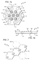
- FIG.1a is a top plan view of a light emitting device or array according to one embodiment of the present invention.
- FIG.1b is a side view of a light emitting device according to one embodiment of the present invention.
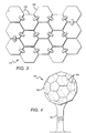
- FIG. 2 is a top plan view of a plurality of LED array elements arranged in a tiling on a flat surface according to one embodiment of the present invention.
- FIG. 3 is a top plan view of a plurality of LED array elements arranged in a tiling on a flat surface according to one embodiment of the present invention.
- FIG.4 is a perspective view of a plurality of LED array elements arranged in a tiling on a three-dimensional surface according to one embodiment of the present invention.
- FIG. 5a is a perspective view of another light emitting device or array according to the present invention.
- FIG. 5b is a plan view of the submount and conductive features for the device shown in FIG. 5a .
- FIG. 5c is a plan view of the submount shown in FIG. 5b with a solder mask.
- FIG. 5d is a perspective view of the device shown in FIG. 5a with secondary optics.
- FIG. 5e is plan view of the device shown in FIG. 5a with secondary optics.
- FIG. 5f is a sectional view of the device shown in FIG. 5e taken along section lines 5e - 5e.
- FIG. 6a is a perspective view of a submount that can be used in another embodiment of light emitting device or array according to the present invention.
- FIG. 6b is a perspective view of another embodiment of a light emitting device or array according to the present invention.
- FIG. 7 is a plan view of one embodiment of a light source utilizing arrays according to the present invention.
- FIG. 8 is one embodiment of a lamp that can utilize arrays according to the present invention.
- FIG. 9 is a flow diagram of one embodiment of a method of fabricating a light emitting device or array according to the present invention.
- the present invention is directed to compact, simple and efficient light emitting devices or arrays and methods for manufacturing same.
- Each array can comprise a submount with a plurality of LEDs coupled together to emit light simultaneously when an electrical signal is applied to the array.
- the arrays according to the present invention can include features to provide for improved thermal management including spreading heat from the LED into the submount from where the heat can then dissipate into a heat sink attached at the bottom of device or the ambient. This allows the arrays to operate under higher power and emit higher luminous flux without overheating.
- the submounts of the arrays are shaped so that multiple arrays can be mounted closely together and electrically connected to form a light source wherein all the arrays emit light in response to an electrical signal. Depending on the requirements for the particular application, different numbers of arrays can be coupled together.
- Arrays according to the present invention can also comprise lenses molded directly over their LEDs to protect the LED while still allowing for efficient emission characteristics. Secondary optics can also be included over the lenses to further shape or disperse the LED light.
- the present invention is also directed to methods for fabricating arrays that generally comprise molding lenses directly over the LEDs on the arrays.
- first, second, etc. may be used herein to describe various elements, components, regions, layers and/or sections, these elements, components, regions, layers and/or sections should not be limited by these terms. These terms are only used to distinguish one element, component, region, layer or section from another region, layer or section. Thus, a first element, component, region, layer or section discussed below could be termed a second element, component, region, layer or section without departing from the teachings of the present invention.
- Embodiments of the invention are described herein with reference to cross-sectional view illustrations that are schematic illustrations of idealized embodiments of the invention. As such, variations from the shapes of the illustrations as a result, for example, of manufacturing techniques and/or tolerances are expected. Embodiments of the invention should not be construed as limited to the particular shapes of the regions illustrated herein but are to include deviations in shapes that result, for example, from manufacturing. A region illustrated or described as square or rectangular will typically have rounded or curved features due to normal manufacturing tolerances. Thus, the regions illustrated in the figures are schematic in nature and their shapes are not intended to illustrate the precise shape of a region of a device and are not intended to limit the scope of the invention.
- the present invention can be used with many different solid state emitters with the embodiments of the invention below being described in relation to LEDs, and in particular to white emitting LEDs.
- the lighting devices or arrays utilizing the white emitting LEDs provide a white emitting light source. It is understood however that different LEDs emitting at different colors can also be used, so that the array emits the color from its LEDS. It is also understood that different colors of LEDs can be used in a single array to generate the desired color of light. For example, red emitting LEDs can be combined with white emitting LEDs so that the array emits a warm white light.
- the present invention can also be used in many different applications and the discussion of the present invention with reference to the following embodiment should not be construed as limiting to the that particular embodiment or similar embodiments.
- FIG. 1a shows one embodiment of a light emitting device or array 100 according to the present invention.
- Light emitting array 100 can serve as an array element when linking several of the devices together to increase luminescent output.
- Substrate/submount 102 comprises top surface 104 and a bottom surface (not shown).
- Various electronic and optical components can be mounted to top surface 104 including at least one light emitting element 106.
- a plurality of light emitting elements 106 are included on the submount 102.
- Such components may include vertical cavity surface emitting lasers (VCSELs), light emitting diodes (LEDs), or other semiconductor devices.
- the element 106 comprises an LED.
- LED structures and their fabrication and operation are generally known in the art and only briefly discussed herein.
- the layers of an LED can be fabricated using known processes with a suitable process being fabrication using metal organic chemical vapor deposition (MOCVD).
- MOCVD metal organic chemical vapor deposition
- the layers of LEDs generally comprise an active layer/region sandwiched between first and second oppositely doped epitaxial layers all of which are formed successively on a growth substrate. LEDs can be formed on a wafer and then singulated for mounting in a package. It is understood that the growth substrate can remain as part of the final singulated LED or the growth substrate can be fully or partially removed.
- the active region can comprise single quantum well (SQW), multiple quantum well (MQW), double heterostructure or super lattice structures.
- SQW single quantum well
- MQW multiple quantum well
- the active region and doped layers may be fabricated from different material systems, with preferred material systems being Group-III nitride based material systems.
- Group-III nitrides refer to those semiconductor compounds formed between nitrogen and the elements in the Group III of the periodic table, usually aluminum (Al), gallium (Ga), and indium (In).
- the term also refers to ternary and quaternary compounds such as aluminum gallium nitride (AlGaN) and aluminum indium gallium nitride (AlInGaN).
- the doped layers are gallium nitride (GaN) and the active region is InGaN.
- the doped layers may be AlGaN, aluminum gallium arsenide (AlGaAs) or aluminum gallium indium arsenide phosphide (AlGaInAsP).
- the growth substrate can be made of many materials such at sapphire, silicon carbide, aluminum nitride (AlN), GaN, with a suitable substrate being a 4H polytype of silicon carbide, although other silicon carbide polytypes can also be used including 3C, 6H and 15R polytypes.
- Silicon carbide has certain advantages, such as a closer crystal lattice match to Group III nitrides than sapphire and results in Group III nitride films of higher quality. Silicon carbide also has a very high thermal conductivity so that the total output power of Group-III nitride devices on silicon carbide are typically not limited by the thermal dissipation of the substrate (as may be the case with some devices formed on sapphire).
- SiC substrates are available from Cree Research, Inc., of Durham, North Carolina and methods for producing them are set forth in the scientific literature as well as in a U.S. Patents, Nos. Re. 34,861 ; 4,946,547 ; and 5,200,022 .
- the LED can also comprise a conductive current spreading structure and one or more wire bond pads on its top surface, both of which are made of a conductive material and can be deposited using known methods. Some materials that can be used for these elements include Au, Cu, Ni, In, Al, Ag or combinations thereof and conducting oxides and transparent conducting oxides.
- the current spreading structure generally comprises conductive fingers arranged in a grid on the LED with the fingers spaced to enhance current spreading from the pads into the LED's top surface. In operation, an electrical signal is applied to the pads through a wire bond as described below, and the electrical signal spreads through the fingers of the current spreading structure and the top surface into the LED. Current spreading structures are often used in LEDs where the top surface is p-type, but can also be used for n-type materials.
- the LED can be coated with one or more phosphors with the phosphors absorbing at least some of the LED light and emitting a different wavelength of light such that the LED emits a combination of light from the LED and the phosphor.
- the LED emits a white light combination of LED and phosphor light.
- the LED can be coated using many different methods, with one suitable method being described in U.S. Patent Applications Serial Nos. 11/656,759 and 11/899,790 , both entitled "Wafer Level Phosphor Coating Method and Devices Fabricated Utilizing Method", and both of which are incorporated herein by reference.
- the LEDs can be coated using other methods such as electrophoretic deposition (EPD), with a suitable EPD method described in U.S.
- LED packages according to the present invention can also have multiple LEDs of different colors, one or more of which may be white emitting.
- the light emitting elements 106 are mounted to top surface 104 and are shown connected in series via conductive features or traces 108 which is disposed on top surface 104.
- the traces 108 can be made of different conductive materials such as metals.
- the light emitting elements 106 can also be connected in a parallel configuration or in a combination of series and parallel connections.
- Input terminal 110 is located near the edge of submount 102.
- Output terminal 112 is located near the opposite edges of submount 102 across from input terminal 110.
- Current from a power source (not shown) flows from input terminal 110 through light emitting elements 106 to output terminal 112, illuminating the array 100.
- Submount 102 can have many different shapes with a preferred shape being a regular hexagon. However, submount 102 may also be shaped as a regular polygon such as a square, a pentagon, etc. Submount 102 may also be shaped as an irregular polygon. Submount 102 as shown in FIG.1a is a regular hexagon having six edges of equal length.
- input terminal 110 is disposed along three adjacent edges. Input terminal 110 comprises three input contact pads 114, each of which is located near to a corresponding one of the three input-side edges.
- Output terminal 112 comprises three output contact pads 116 which are located near the three adjacent edges on the output-side, opposite the input terminal 110.
- the input and output contact pads 114, 116 are disposed on top surface 104 along the edges to provide easy access to the input and output terminals 110, 112. This allows for flexibility when designing an array layout to connect several light emitting array elements.
- light emitting elements 106 may be mounted to top surface 104 and can be arranged in many different configurations on top surface 104.
- the light emitting elements can be connected in parallel, in series, or in a combination of both to achieve optimal light output.
- a preferred pattern comprises seven light emitting elements 106 arranged in a serial serpentine pattern as shown in FIG.1a . Current flows from input contact pad 114 through all of the light emitting elements 106 to output contact pad 116.
- Bore holes 118 are disposed near opposite vertices between the outer input and output contact pads 114, 116. Bore holes 118 are used to facilitate mounting the devices to a surface. They can be sized to accommodate a variety of screws or mounting pins.
- FIG. 1b is a side front view of a light emitting array 100 according to one embodiment of the present invention.
- Light emitting array 100 has a top surface 104 and a bottom surface 132.
- Lighting elements 106 are mounted to top surface and electrically connected.
- FIG. 1b illustrates one such design.
- Heat spreader 134 has a high thermal conductivity over a broad range of temperatures and is disposed beneath top surface 104. Heat spreader 134 may be made from copper, aluminum and ceramic, for example; although it could also be made from any high thermal conductivity material. In the design shown in FIG.1b , heat spreader 134 forms the bottom surface 132 of the device.
- the embodiment of light emitting array 100 as illustrated in FIG.1b is oriented such that input terminal 110 (not visible in this view) is on the left-hand side of the figure as indicated by the positive sign (+). Likewise the output terminal 112 (not visible in this view) is on the right-hand as indicated by the negative sign (-). In this embodiment viewed from this orientation, an output contact pad 116 (not visible in this view) is disposed near the front edge.
- Bore holes 136 are shown with dshed lines to indicate that they are set off a distance from the front edge of array 100.
- the holes 136 pass through top and bottom surfaces 104, 132, allowing array 100 to be easily mounted to other surfaces.
- devices 100 can be mounted to a surface in several different ways including but not limited to methods using screws, epoxy adhesives and solders.
- FIG.2 is a top plan view of a light source 150 according to the present invention having three light emitting devices or arrays 152, 154, 156 according to one embodiment of the present invention.
- Devices 152, 154, 156 are connected in a serial arrangement. The arrows indicate the direction of current flow through the devices. Current flows into 152 at one of the edges marked with a positive (+). The current then flows through the light emitters (not shown), out of device 152 at one of the edges marked with a negative sign (-), and into one of the positive edges of device 154.
- Device 156 is shown positioned adjacent to the middle negative edge of device 154.
- device 156 can also be disposed in either of two alternate positions 158 (shown with hashed lines). Because the positive and negative terminals are easily accessible from multiple sides of each device, there is a great deal of flexibility in designing the layout of the devices in an array and the path through which current will flow.
- the layout of FIG.2 is just one simple example of an array of devices and is meant to illustrate the additional freedom of design afforded by various embodiments of the invention.
- One of skill in the art will recognize that the devices can be easily rotated, shifted and expanded to achieve a desired layout and current flow. An example of such an array is described below and illustrated in FIG.3 .
- FIG.3 is a top plan view of an array 170 of light emitting devices 100 according to one embodiment of the present invention.
- Devices 100 function as array elements and are arranged in a tiling which can be expanded in all directions to accommodate luminescent output requirements.
- Devices 100 are oriented such that edges of the respective devices that face each other are parallel. Spacing between the devices 100 can vary according to design specifications, for example, to accommodate different types of conductors.
- the devices 100 are mounted on a flat surface.
- the design engineer has a great deal of flexibility in arranging the array elements.
- the array can be expanded in any direction, allowing for various circuit connection schemes and increasing output efficiency.
- array elements having different shapes such as squares, pentagons, or octagons, for example. Combinations of such shapes may also be used to develop a specific array layout.
- FIG.4 is a perspective view of a three-dimensional (3-D) array 180 of light emitting devices 184 according to one embodiment of the present invention.
- Devices 184 may be mounted to the surface of a 3-D structure 182 to achieve omnidirectional luminescence.
- This particular embodiment comprises hexagonal and pentagonal array elements 184 that correspond to the substantially spherical 3-D structure 182 on which the devices 184 are mounted.
- the structure 182 is mounted on a support 186.
- Current may be delivered from a power source (not shown) either external to the structure 182 or from within the structure 182 or the support 186.
- a power source external to the structure 182.
- Current flows through some or all of the array elements 184 and back out of the structure 182 as shown by the polarity arrows.
- Alternate embodiments may include structures having any 3-D shape. Array elements that are mounted to those structures may also come in any shape in order to efficiently cover part or all of the surface of the structure.
- FIGs. 5a through 5f show another embodiment of a light emitting device or array 200 comprising a substrate/submount 202 having a top surface 204 and bottom surface 206.
- the substrate/submount can be made of many different structures and materials such as a printed circuit board (PCB), metal core printed circuit board (MCPCB).
- PCB printed circuit board
- MCPCB metal core printed circuit board
- suitable materials include, but are not limited to ceramic materials such as aluminum oxide, aluminum nitride or organic insulators like polyimide(PI) and polyphthalamide(PPA) laminated with thermally and electrically conductive materials such as copper or other similar materials.
- the submount 202 can comprise a printed circuit board (PCB), sapphire or silicon or any other suitable material, such as T-Clad thermal clad insulated substrate material, available from The Bergquist Company of Chanhassen, Minn.
- PCB printed circuit board
- sapphire or silicon
- any other suitable material such as T-Clad thermal clad insulated substrate material, available from The Bergquist Company of Chanhassen, Minn.
- T-Clad thermal clad insulated substrate material available from The Bergquist Company of Chanhassen, Minn.
- PCB printed circuit board
- sapphire or silicon any other suitable material, such as T-Clad thermal clad insulated substrate material, available from The Bergquist Company of Chanhassen, Minn.
- T-Clad thermal clad insulated substrate material available from The Bergquist Company of Chanhassen, Minn.
- different PCB types can be used such as standard FR-4 PCB, metal core PCB, or any other type of printed circuit
- arrays according to the present invention can be fabricated using a method that utilizes a submount panel sized to accommodate a plurality of arrays. Multiple arrays can be formed on the panel, with the individual arrays being singulated from the panel. In other embodiments the arrays can be fabricated from separate submounts instead of a panel of submounts.
- the submount's top surface 204 comprises patterned conductive features 208 that can include a plurality of die attach pads 210 and interconnecting conductive traces 212.
- a plurality of LEDs 214 are provided that can be the same as the LEDs described above with reference to element 106 in FIGs. 1 and 2 .
- Each of the LEDs 214 are mounted to a respective one of the attach pads, with each approximately at the center of its pad 210. It is understood that in alternative embodiments multiple LEDs can be mounted to each of the respective one of the attached pads, with the LEDs emitting the same or different colors of light.
- Each of the LEDs can be electrically interconnected in a combination of serial and/or parallel connections.
- the LEDs on at least some of the attach pads can be connected in parallel, such that the array comprises a serial connection between the pads with the attach pads having a parallel connection.
- the patterned conductive features 208 provide conductive paths for electrical connection to the LEDs 214 using known contacting methods.
- the LEDs can be mounted to the attach pads 210 using known methods and materials such as using conventional solder materials that may or may not contain a flux material, or dispensed polymeric materials that may be thermally and electrically conductive.
- the attach pads 210 and traces 212 can comprise different materials such as metals or other conductive materials.
- the pads 210 and traces 212 can comprise copper deposited using known techniques such as plating. In typical plating processes a titanium adhesion layer and copper seed layer are sequentially sputtered onto a substrate. Then, approximately 75 microns of copper is plated onto the copper seed layer. The resulting copper layer being deposited can then be patterned using standard lithographic processes. In other embodiments the layer can be sputtered using a mask to form the desired pattern.
- some of the conductive features 208 can include only copper, with others of the features including additional materials.
- the attach pads 210 can be plated or coated with additional metals or materials to the make each more suitable for mounting LEDs 214.
- the attach pads 210 can be plated with adhesive or bonding materials, or reflective and barrier layers.
- a wire bond (not shown) can be included between each LED 214 and an adjacent one of the traces 212 such that all the LEDs are connected in series between the pads 210 and the traces 212.
- Other methods to connect the LEDs on the attach pad 210 with the traces 212 can comprise a flip-chip bonded LED with co-planar metal contacts (e.g. stud bumps) on the LED providing the connection between the attach pad 210, the traces 212, and the LED diode contacts.
- the conductive features 208 can also comprise input and output contact pads 216, 218, that can be made of the same materials and deposited in the same way as the other conductive features.
- the contact pads 216, 218 are typically on opposing sides of the submount with the input contact pad 216 coupled to a trace 212 leading to the first in the series of attach pads 210, and the output contact pad 218 coupled to the last in the series attach pads.
- a signal applied to the input contact pad 216 conducts through each of the LEDs 214, attach pads 210 and interconnecting traces 212, to the output contact pad 218.
- the signal could then be transmitted to another similar array 200 using known jumper methods.
- the attach pads 210 can provide thermally conductive paths to conduct heat away from the LEDs 214 such that heat can spread to other areas of the submount beyond the areas just below the LEDs 214.
- the attach pads 210 cover more of the surface of the top surface 204 than the LEDs 214, with the attach pads extending from the edges of the LEDs 214.
- each of the attach pads 210 are generally circular and extend radially from its respective one of the LEDs 214. It is understood that the contact pads 216, 218 can be many other shapes and in some embodiments it can extend further on the submount's top surface to improve thermal dissipation of heat generated in the LED 214.
- the submount 202 comprises a metal core printed circuit board
- adequate levels of heat can spread from the attach pads 210 through the submount 202.
- the submount comprises a material that is less thermally conductive, such as a ceramic
- additional elements can be included to further assist in heat dissipation.
- the submount's bottom surface 206 can comprise a separate thermal pad or sets of thermal pads that can be in vertical alignment with the attach pads on the top surface. The bottom thermal pads serve to dissipate heat or conduct heat to heat sink from where head is dissipated into the ambient.
- the metalized area can assist with this dissipation by allowing this heat to spread into the metalized area where it can dissipate more readily.
- the metalized layer can be made of known thermally conductive materials, such as metals, deposited using known techniques.
- the array can be arranged for surface mounting by having surface mount contacts (not shown) on the submount's bottom surface 206.
- the input and output contact pads 216, 218 can also be connected to the submount bottom surface using electrically conductive via connections.
- the arrays can be interconnected by using known printed circuit board and surface mount technology.
- the surface mount contacts are arranged to be compatible with surface mount processes, and can be in electrical contact with the conductive features on the submount's top surface 204.
- conductive vias can be included through the submount to provide this electrical connection.
- An optical elements or lenses 220 are formed on the submount's top surface 204, with each of the lenses being over a respective one of the LEDs 214 to provide both environmental and/or mechanical protection.
- the lenses 220 can be in different locations on the top surface 204 with the lenses located as shown with their respective one of the LEDs 214 at approximately the center of the lens base.
- each or some of the lenses 220 can be formed in direct contact with its one of the LEDs 214 and the submount's top surface 204. In other embodiments there may be an intervening material or layer between the LED 220 and/or top surface 204. Direct contact to the LED 214 provides certain advantages such as improved light extraction and ease of fabricating.
- the lenses 220 can be molded over the LEDs 214 using different molding techniques and the lens can be many different shapes depending on the desired shape of the light output.
- One suitable shape as shown is hemispheric, with some examples of alternative shapes being ellipsoid bullet, flat, hex-shaped and square.
- Many different materials can be used for the lens such as silicones, plastics, epoxies or glass, with a suitable material being compatible with molding processes. Silicone is suitable for molding and provides suitable optical transmission properties. It can also withstand subsequent reflow processes and does not significantly degrade over time. It is understood that one or more of the lenses 220 can also be textured to improve light extraction or can contain materials such as phosphors or scattering particles.
- the array can also comprise a protective layer (not shown) covering the submount's top surface 204 not covered by the lenses 220.
- the protective layer can provide additional protection to the elements on the top surface 204 to reduce damage and contamination during subsequent processing steps and use.
- the protective layer can be formed during formation of the lenses 220 and can comprise the same material as the lenses 220. Openings should be formed in the protective layer to provide access to the first and second contact pads 216, 218, with the openings formed using known processes.
- the arrangement of the lenses 220 is also easily adapted for use with secondary optics 222 that can be included over the lenses during fabrication of the array 200 or by the end user.
- the optics 222 can be included for different purposes such as to facilitate beam shaping or beam dispersion.
- Secondary optics are generally known in the art, with many of them being commercially available. They can be formed from many different materials such as plastics (PMMA, PC) and can be formed from processes such as injection molding. In other embodiments the lenses can be made of glass and can also be formed using known methods.
- the optics 222 can be integrated into a single assembly (as shown) that mounts as one piece over the lenses 220, or in other embodiments the optics can comprise individual pieces, each of which is mounted over a respective one of the lenses 220.
- the optics 222 can be mounted over the lenses using known mounting and bonding techniques.
- the array 200 also comprises registration thru-holes 224 arranged to assist in aligning the secondary optics 222 to the array 200 during mounting of the optics.
- Lockdown thru-holes 226 are also included for mounting the array 200 in place for use, such as to a heat sink in a lamp.
- the array 200 can also comprise elements to protect against damage from electrostatic discharge (ESD). These elements (not shown) can be mounted to the submount 202, and different elements can be used such as various vertical silicon (Si) Zener diodes, different LEDs arranged in parallel and reverse biased to the LEDs, surface mount varistors and lateral Si diodes.
- ESD electrostatic discharge
- a solder mask 236 can be included on the submount's top surface 204, at least partially over the attach pads 210 and the first and second contact pads 216, 218, and covering the traces 212.
- the solder mask 236 protects these features during subsequent processing steps and in particular mounting the LEDs 214 to the attach pads 210 and wire bonding. During these steps there can be a danger of solder or other materials depositing in undesired areas, which can result in damage to the areas or result in electrical shorting.
- the solder mask serves as an insulating and protective material that can reduce or prevent these dangers. It may also serve to promote the adhesion of the lenses to the submount surface 204.
- the solder mask comprises opening for mounting the LEDs 214 to the attach pads 210 and for attaching wire bonds to the traces 212. It also comprises side openings on the contact pads 216, 218 for connecting jumpers between adjacent arrays.
- FIGs. 6a and 6b show another embodiment of an array 250 according to the present invention having a submount 252 similar to the submount 102 shown in FIGs. 1-3 and described above, but also comprises molded lenses.
- the submount 252 has a top surface 254 having electrically conductive features 256 comprising die attach pads 258, interconnecting traces 260.
- LEDs 261 are mounted to the attach pads 258 as described above and electrically connected to their adjacent traces 260, so that the LEDs are connected in series or in parallel (not shown).
- the attach pads 258 are arranged to extend on the top surface of the submount 252 to facilitate lateral heat spreading from the LEDs 261, and to allow the heat to spread into the submount where it can dissipate.
- First and second contact pads 262, 264 are arranged on the top surface 254 to provide access to each of the pads 262, 264 from three edges of the submount 252. This provides flexibility in connecting several luminaries in an array.
- the array 250 further comprises lenses 266 and secondary optics 268 similar to the lenses 220 and secondary optics 222 described above in conjunction with FIGs. 5a through 5f .
- the array 250 can also comprise lock down thru holes for mounting by the end user, such as in a lamp.
- Contact pads 262, 264 are around three edges of the submount 252, which leaves less area for the attach pads around the edges. Accordingly, for these embodiments the attach pads can be located closer to the center of the submount compared to those embodiments not having contacts around the edges.
- Arrays according to the present invention can be arranged in many different ways from the arrays 100, 200, 250 described above, and can be include different elements or components beyond those described above.
- electrical drive circuits or electrical conditioning circuits can be included on the array either as discrete or integrated components.
- the arrays can also comprise other elements to enhance heat spreading such as heat fins or various heat sinks. Accordingly, the present invention should not be construed as limited to the embodiments shown and described.
- FIG.7 shows one embodiment of a light source 300 comprising luminaries 302 that are similar to those described above and shown in FIGs. 5a through 5f .
- Jumpers (not shown) can be included between contact pads of adjacent arrays 302, so that an electrical signal applied the first of the arrays 302 is conducted to the others.
- the interconnected arrays 302 are preferably mounted to a surface 304 that can also serve as a heat sink to draw heat away from the arrays.
- the light source 300 can be used in many different lighting applications, with one being the light source for a lamp.
- FIG. 8 shows one embodiment of a lamp 350 that can use the light source 300 and other array based light sources.
- the light source 300 is arranged within the lamp housing 352 so that light emits out through the housing opening 354.
- the opening 354 can have a cover to protect the light source 300 or an opening optical element to both protect the light source and shape the emitting light.
- the housing 352 can have heat dissipating fins 356 to help dissipate the heat from the light source 300.
- the light source 300 can be arranged to emit many different colors of light with different intensities. Different LEDs can be used on the arrays 302 for different colors and temperatures of light. In one embodiment the light source can emit 1000 lumens or more. In embodiments having LEDs emitting cool white light, the light source 300 emits at 4000 to 10,000 correlated color temperature (CCT). In embodiments where the arrays have LEDs emitting warm white light, the light source 300 emits at 2700 to 4000K CCT. The white light source can also have a color rendering index of 80 or greater.
- the lamp 350 can also be provided with an integrated power supply that allows it to operate with an efficiency of 90 lumens per Watt or greater.
- FIG. 9 shows one embodiment of an LED package fabrication method 400 according to the present invention.
- a substrate (submount) is provided that can have many different shapes but is preferably hexagon shaped, and sized to serve as the submount for a single array.
- a submount panel can be provided sized so that it can be diced in subsequent manufacturing steps to provide a plurality of individual submounts. This allows for simultaneous fabrication of a plurality of packages.
- a separate processing step is required for providing the conductive features either for the individual submount or for the panel.
- These features can include the attach pad, traces, contact pads and metalized are, some of which can be arranged to assist in dissipating heat generated by the LED as described above.
- the panel comprises a plurality of these features arranged in sets, each of the sets corresponding to one of the plurality of arrays to be formed from the panel.
- a plurality of LEDs are provided each of which is to be die attached to a respective one of the attach pads.
- the plurality of LEDs comprise white emitting LEDs chips, and many different white chips can be used with a suitable white chip being described in the patent applications mentioned above and incorporated herein.
- more than one LED can be provided for mounting to each of the attach pads.
- a plurality of ESD protection elements can also be provided, each of which can be mounted in conjunction with one of the attach pads to provide ESD protection for the LEDs. Many different mounting methods and materials can be used, such as mounting using conventional solder materials and methods.
- each of the ESD elements can also be mounted to a respective attach pad using the same mounting method and material. It is understood that the ESD element can also be mounted in other locations using other methods.
- electrical connections are formed between each of the LEDs on the attach pads and one of the adjacent traces so that the LEDs are connected in series between the attach pads.
- the ESD element can also be connected to the respective trace.
- Wire bond connections can be formed using known processes and can be made of known conductive materials such as gold. It is understood that flip-chip bonded LED or ESD elements with co-planar contacts to their respective electrodes can also be used as an alternative method for connecting the devices to the traces. Other methods include eutectic attach and solder attach processes.
- the LEDs can be provided and mounted to the panel without the desired white light conversion material.
- the conversion material can be deposited on the LED after wire bonding.
- the conversion material or phosphor is deposited on the LED, and many different known phosphor deposition methods can be used such as electrophoretic deposition (EPD), with a suitable EPD process described in the patent application mentioned above.
- the first encapsulant is formed over the LEDs by molding over each of the LEDs and many different molding methods can be used.
- a molding process is used that simultaneously forms lenses over the LEDs submount (or submount panel).
- One such molding process is referred to as compression molding processes wherein a mold is provided having a plurality of cavities each of which has an inverted shape of the lens. Each cavity is arranged to align with a respective one of the LEDs on a submount.
- the mold is loaded with a lens material in liquid form filling the cavities, with the preferred material being liquid curable silicone.
- the submount is inverted and moved toward the cavity with each of the LEDs being embedded in the liquid silicone within one a respective one of the cavities.
- a layer of silicone can also remain between adjacent lenses that provides a protective layer over the top surface of the submount.
- the liquid silicone can then be cured using known curing processes.
- the submount can then be removed from the mold and the submount can comprise a plurality of molded lenses, each of which is over a respective one of the LEDs.
- the lenses can be formed over the LEDs using known dispensing processing and then cured.
- optional 412 can be utilized to singulate the submount panel into individual arrays.
- an optical element can be mounted over the lenses in the form of secondary optics. These optics can be made of the materials described above, can be fabricated using the methods described above, and can be mounted over the lenses using known methods and materials.
- each of the arrays can be tested to be sure they are operating correctly and to measure each device output light characteristics.
- the LED packages can be shipped to the customer.
- the panel can be diced/singulated to separate the individual arrays and different methods can be used such as known saw singulation methods.
- a tape can be attached to the panel prior to singulation to hold and stabilize the panel and individual arrays. Following singulation, the arrays can be cleaned and dried.
Landscapes
- Engineering & Computer Science (AREA)
- General Engineering & Computer Science (AREA)
- Physics & Mathematics (AREA)
- Microelectronics & Electronic Packaging (AREA)
- Optics & Photonics (AREA)
- Led Device Packages (AREA)
- Devices For Indicating Variable Information By Combining Individual Elements (AREA)
- Led Devices (AREA)
Applications Claiming Priority (1)
| Application Number | Priority Date | Filing Date | Title |
|---|---|---|---|
| US11/982,276 US10295147B2 (en) | 2006-11-09 | 2007-10-31 | LED array and method for fabricating same |
Publications (3)
| Publication Number | Publication Date |
|---|---|
| EP2056014A2 true EP2056014A2 (fr) | 2009-05-06 |
| EP2056014A3 EP2056014A3 (fr) | 2014-04-02 |
| EP2056014B1 EP2056014B1 (fr) | 2018-08-01 |
Family
ID=40328464
Family Applications (1)
| Application Number | Title | Priority Date | Filing Date |
|---|---|---|---|
| EP08252829.0A Active EP2056014B1 (fr) | 2007-10-31 | 2008-08-27 | Réseau de DEL et procédé de fabrication de celui-ci |
Country Status (3)
| Country | Link |
|---|---|
| US (1) | US10295147B2 (fr) |
| EP (1) | EP2056014B1 (fr) |
| JP (1) | JP2009111346A (fr) |
Cited By (9)
| Publication number | Priority date | Publication date | Assignee | Title |
|---|---|---|---|---|
| GB2473185A (en) * | 2009-08-28 | 2011-03-09 | Ocean Led Ltd | Luminaire formed from PCB and cover. |
| WO2011051310A1 (fr) * | 2009-10-27 | 2011-05-05 | Ceramtec Gmbh | Matrice de supports en céramique modulables munis de diodes électroluminescentes |
| GB2476678A (en) * | 2010-01-05 | 2011-07-06 | Led Semiconductor Co Ltd | Polygonal light emitting diode module assembly |
| WO2011124666A3 (fr) * | 2010-04-09 | 2012-02-02 | Tridonic Jennersdorf Gmbh | Module de led pour des spots |
| WO2012101547A1 (fr) * | 2011-01-25 | 2012-08-02 | Koninklijke Philips Electronics N.V. | Ensemble modulaire à base de diodes électroluminescentes |
| GB2497283A (en) * | 2011-12-02 | 2013-06-12 | Tzu-Yu Liao | Method for assembling LEDs to a ceramic heat conductive member |
| CN103307477A (zh) * | 2012-01-31 | 2013-09-18 | Lg伊诺特有限公司 | 照明装置 |
| US9353914B2 (en) | 2011-09-02 | 2016-05-31 | Lg Innotek Co., Ltd. | Lighting device |
| USRE47425E1 (en) | 2012-05-07 | 2019-06-04 | Lg Innotek Co., Ltd. | Lighting device having reflectors for indirect light emission |
Families Citing this family (108)
| Publication number | Priority date | Publication date | Assignee | Title |
|---|---|---|---|---|
| US9793247B2 (en) * | 2005-01-10 | 2017-10-17 | Cree, Inc. | Solid state lighting component |
| US7564180B2 (en) | 2005-01-10 | 2009-07-21 | Cree, Inc. | Light emission device and method utilizing multiple emitters and multiple phosphors |
| US9070850B2 (en) | 2007-10-31 | 2015-06-30 | Cree, Inc. | Light emitting diode package and method for fabricating same |
| US7821023B2 (en) | 2005-01-10 | 2010-10-26 | Cree, Inc. | Solid state lighting component |
| US8125137B2 (en) | 2005-01-10 | 2012-02-28 | Cree, Inc. | Multi-chip light emitting device lamps for providing high-CRI warm white light and light fixtures including the same |
| DE102005043819A1 (de) * | 2005-09-13 | 2007-03-29 | Doctor Optics Gmbh | Scheinwerferlinse für einen Kraftfahrzeugscheinwerfer |
| EP1963743B1 (fr) | 2005-12-21 | 2016-09-07 | Cree, Inc. | Dispositif d'eclairage |
| EP2372223A3 (fr) | 2005-12-21 | 2012-08-01 | Cree, Inc. | Dispositif d'éclairage et procédé d'éclairage |
| EP1969633B1 (fr) | 2005-12-22 | 2018-08-29 | Cree, Inc. | Dispositif d' eclairage |
| US8513875B2 (en) | 2006-04-18 | 2013-08-20 | Cree, Inc. | Lighting device and lighting method |
| US9084328B2 (en) | 2006-12-01 | 2015-07-14 | Cree, Inc. | Lighting device and lighting method |
| US9335006B2 (en) * | 2006-04-18 | 2016-05-10 | Cree, Inc. | Saturated yellow phosphor converted LED and blue converted red LED |
| EP2052589A4 (fr) | 2006-04-18 | 2012-09-19 | Cree Inc | Dispositif et procede d'eclairage |
| KR101517244B1 (ko) | 2006-04-20 | 2015-05-04 | 크리, 인코포레이티드 | 조명 기기 및 조명 방법 |
| US8596819B2 (en) | 2006-05-31 | 2013-12-03 | Cree, Inc. | Lighting device and method of lighting |
| US9443903B2 (en) | 2006-06-30 | 2016-09-13 | Cree, Inc. | Low temperature high strength metal stack for die attachment |
| US8698184B2 (en) * | 2011-01-21 | 2014-04-15 | Cree, Inc. | Light emitting diodes with low junction temperature and solid state backlight components including light emitting diodes with low junction temperature |
| US7665862B2 (en) * | 2006-09-12 | 2010-02-23 | Cree, Inc. | LED lighting fixture |
| US7766508B2 (en) * | 2006-09-12 | 2010-08-03 | Cree, Inc. | LED lighting fixture |
| US8029155B2 (en) | 2006-11-07 | 2011-10-04 | Cree, Inc. | Lighting device and lighting method |
| US10295147B2 (en) | 2006-11-09 | 2019-05-21 | Cree, Inc. | LED array and method for fabricating same |
| US9441793B2 (en) | 2006-12-01 | 2016-09-13 | Cree, Inc. | High efficiency lighting device including one or more solid state light emitters, and method of lighting |
| KR20080049947A (ko) * | 2006-12-01 | 2008-06-05 | 엘지전자 주식회사 | 방송 시스템, 인터페이스 방법, 및 데이터 구조 |
| EP2089654B1 (fr) | 2006-12-07 | 2016-08-03 | Cree, Inc. | Dispositif et procédé d'éclairage |
| US8258682B2 (en) * | 2007-02-12 | 2012-09-04 | Cree, Inc. | High thermal conductivity packaging for solid state light emitting apparatus and associated assembling methods |
| KR101499269B1 (ko) | 2007-02-22 | 2015-03-09 | 크리, 인코포레이티드 | 발광 장치, 발광 방법, 광 필터 및 광 필터링 방법 |
| US7824070B2 (en) | 2007-03-22 | 2010-11-02 | Cree, Inc. | LED lighting fixture |
| US7896521B2 (en) * | 2007-05-04 | 2011-03-01 | Abl Ip Holding Llc | Adjustable light distribution system |
| WO2008137975A1 (fr) | 2007-05-08 | 2008-11-13 | Cree Led Lighting Solutions, Inc. | Dispositif et procédé d'éclairage |
| KR20100020464A (ko) | 2007-05-08 | 2010-02-22 | 크리 엘이디 라이팅 솔루션즈, 인크. | 조명 장치 및 조명 방법 |
| US7901107B2 (en) | 2007-05-08 | 2011-03-08 | Cree, Inc. | Lighting device and lighting method |
| KR101460832B1 (ko) | 2007-05-08 | 2014-11-12 | 크리, 인코포레이티드 | 조명 장치 및 조명 방법 |
| TWI422785B (zh) | 2007-05-08 | 2014-01-11 | 克里公司 | 照明裝置及照明方法 |
| US20090002979A1 (en) * | 2007-06-27 | 2009-01-01 | Cree, Inc. | Light emitting device (led) lighting systems for emitting light in multiple directions and related methods |
| US8042971B2 (en) | 2007-06-27 | 2011-10-25 | Cree, Inc. | Light emitting device (LED) lighting systems for emitting light in multiple directions and related methods |
| US7863635B2 (en) | 2007-08-07 | 2011-01-04 | Cree, Inc. | Semiconductor light emitting devices with applied wavelength conversion materials |
| KR101722265B1 (ko) | 2007-10-10 | 2017-03-31 | 크리, 인코포레이티드 | 조명 장치 및 그 제조 방법 |
| US8240875B2 (en) | 2008-06-25 | 2012-08-14 | Cree, Inc. | Solid state linear array modules for general illumination |
| GB2458972B (en) * | 2008-08-05 | 2010-09-01 | Photonstar Led Ltd | Thermally optimised led chip-on-board module |
| US20100046221A1 (en) * | 2008-08-19 | 2010-02-25 | Jason Loomis Posselt | LED Source Adapted for Light Bulbs and the Like |
| DE102008051044A1 (de) * | 2008-10-09 | 2010-04-15 | Osram Opto Semiconductors Gmbh | Optoelektronisches Bauteil |
| US9425172B2 (en) | 2008-10-24 | 2016-08-23 | Cree, Inc. | Light emitter array |
| US8309973B2 (en) * | 2009-02-12 | 2012-11-13 | Taiwan Semiconductor Manufacturing Company, Ltd. | Silicon-based sub-mount for an opto-electronic device |
| US8096671B1 (en) | 2009-04-06 | 2012-01-17 | Nmera, Llc | Light emitting diode illumination system |
| US8921876B2 (en) | 2009-06-02 | 2014-12-30 | Cree, Inc. | Lighting devices with discrete lumiphor-bearing regions within or on a surface of remote elements |
| JP4686625B2 (ja) * | 2009-08-03 | 2011-05-25 | 株式会社東芝 | 半導体発光装置の製造方法 |
| US8598809B2 (en) * | 2009-08-19 | 2013-12-03 | Cree, Inc. | White light color changing solid state lighting and methods |
| JP2011066133A (ja) * | 2009-09-16 | 2011-03-31 | Koito Mfg Co Ltd | 発光モジュール及び車輌用灯具 |
| WO2011033433A1 (fr) * | 2009-09-17 | 2011-03-24 | Koninklijke Philips Electronics N.V. | Module d'éclairage et dispositif électroluminescent |
| US9385285B2 (en) | 2009-09-17 | 2016-07-05 | Koninklijke Philips N.V. | LED module with high index lens |
| WO2011037877A1 (fr) | 2009-09-25 | 2011-03-31 | Cree, Inc. | Dispositif d'éclairage à faible éblouissement et à grande uniformité du niveau de lumière |
| JP5375552B2 (ja) * | 2009-11-24 | 2013-12-25 | 東芝ライテック株式会社 | 発光装置及びこれを備えた照明器具 |
| US8511851B2 (en) * | 2009-12-21 | 2013-08-20 | Cree, Inc. | High CRI adjustable color temperature lighting devices |
| TWM409543U (en) | 2010-01-13 | 2011-08-11 | Molex Inc | Holder assembly |
| US9275979B2 (en) | 2010-03-03 | 2016-03-01 | Cree, Inc. | Enhanced color rendering index emitter through phosphor separation |
| TWM387368U (en) * | 2010-04-29 | 2010-08-21 | Shin Zu Shing Co Ltd | LED module |
| KR101064036B1 (ko) * | 2010-06-01 | 2011-09-08 | 엘지이노텍 주식회사 | 발광 소자 패키지 및 조명 시스템 |
| JP5545848B2 (ja) * | 2010-06-24 | 2014-07-09 | シチズン電子株式会社 | 半導体発光装置 |
| CN103080641A (zh) * | 2010-07-06 | 2013-05-01 | 克利公司 | 具有综合热管理的紧凑光学有效固态光源 |
| US9293678B2 (en) | 2010-07-15 | 2016-03-22 | Micron Technology, Inc. | Solid-state light emitters having substrates with thermal and electrical conductivity enhancements and method of manufacture |
| JP5587095B2 (ja) * | 2010-08-18 | 2014-09-10 | 日東光学株式会社 | レンズ製造システム、レンズアレイおよびled照明装置 |
| US20120074432A1 (en) * | 2010-09-29 | 2012-03-29 | Amtran Technology Co., Ltd | Led package module and manufacturing method thereof |
| TWI472058B (zh) | 2010-10-13 | 2015-02-01 | 英特明光能股份有限公司 | 發光二極體裝置 |
| EP2630408A2 (fr) | 2010-10-21 | 2013-08-28 | Koninklijke Philips Electronics N.V. | Puits de chaleur multifonctionnel de faible coût destiné à des réseaux de diodes électroluminescentes |
| US8455895B2 (en) * | 2010-11-08 | 2013-06-04 | Bridgelux, Inc. | LED-based light source utilizing asymmetric conductors |
| US20150062915A1 (en) * | 2013-09-05 | 2015-03-05 | Cree, Inc. | Light emitting diode devices and methods with reflective material for increased light output |
| IT1402806B1 (it) * | 2010-11-29 | 2013-09-18 | St Microelectronics Srl | Dispositivo fotomoltiplicatore incapsulato di materiale semiconduttore, in particolare per l'utilizzo in macchine per l'esecuzione della tomografia ad emissione di positroni. |
| CN102130239B (zh) * | 2011-01-31 | 2012-11-07 | 郑榕彬 | 全方位采光的led封装方法及led封装件 |
| US9786811B2 (en) | 2011-02-04 | 2017-10-10 | Cree, Inc. | Tilted emission LED array |
| DE102011004086C5 (de) * | 2011-02-14 | 2016-07-14 | Automotive Lighting Reutlingen Gmbh | Verfahren zur Herstellung einer farbkorrigierenden Projektionsoptik |
| US11251164B2 (en) | 2011-02-16 | 2022-02-15 | Creeled, Inc. | Multi-layer conversion material for down conversion in solid state lighting |
| USD700584S1 (en) | 2011-07-06 | 2014-03-04 | Cree, Inc. | LED component |
| US10842016B2 (en) * | 2011-07-06 | 2020-11-17 | Cree, Inc. | Compact optically efficient solid state light source with integrated thermal management |
| JP5866703B2 (ja) * | 2011-07-07 | 2016-02-17 | 株式会社マリンコムズ琉球 | 可視光通信方法及び可視光通信装置 |
| JP5726680B2 (ja) * | 2011-08-29 | 2015-06-03 | 日立アプライアンス株式会社 | Led照明装置 |
| US10043960B2 (en) * | 2011-11-15 | 2018-08-07 | Cree, Inc. | Light emitting diode (LED) packages and related methods |
| US9115876B1 (en) * | 2011-12-30 | 2015-08-25 | Global Tech Led Holdings, Llc | LED light having LED cluster arrangements |
| TWD151017S (zh) * | 2012-01-20 | 2012-12-21 | 隆達電子股份有限公司 | 發光二極體模組 |
| US9863616B2 (en) * | 2012-01-30 | 2018-01-09 | Bridgelux Inc. | Circuit board for LED applications |
| TWD152723S (zh) * | 2012-03-15 | 2013-04-01 | 隆達電子股份有限公司 | 發光二極體模組 |
| DE102012219364A1 (de) | 2012-10-23 | 2014-04-24 | Allnet Gmbh | Verbindbare LED-Module und Verfahren zum Verbinden von LED-Modulen |
| EP2725284A1 (fr) | 2012-10-23 | 2014-04-30 | Allnet GmbH | Modules à DEL interconnectables et procédé d'interconnexion de modules à DEL |
| JP6026315B2 (ja) * | 2013-02-20 | 2016-11-16 | スタンレー電気株式会社 | 発光素子モジュール |
| USD714488S1 (en) * | 2013-02-26 | 2014-09-30 | Shanghai Sansi Electronics Engineering Co., Ltd. | Chessboard shaped LED lamp |
| US10295124B2 (en) * | 2013-02-27 | 2019-05-21 | Cree, Inc. | Light emitter packages and methods |
| WO2014141009A1 (fr) * | 2013-03-15 | 2014-09-18 | Koninklijke Philips N.V. | Structure électroluminescente et monture |
| US9470395B2 (en) | 2013-03-15 | 2016-10-18 | Abl Ip Holding Llc | Optic for a light source |
| US9303821B2 (en) * | 2013-03-29 | 2016-04-05 | Uniled Lighting Tw., Inc. | Air-cooled LED lamp bulb |
| US10807329B2 (en) | 2013-05-10 | 2020-10-20 | Abl Ip Holding Llc | Silicone optics |
| CN104241262B (zh) | 2013-06-14 | 2020-11-06 | 惠州科锐半导体照明有限公司 | 发光装置以及显示装置 |
| TWI556478B (zh) * | 2014-06-30 | 2016-11-01 | 億光電子工業股份有限公司 | 發光二極體裝置 |
| AT516416B1 (de) * | 2014-10-21 | 2019-12-15 | Zkw Group Gmbh | Leiterplatte mit einer Mehrzahl von an der Leiterplatte in zumindest einer Gruppe angeordneter elektronischer Bauteile |
| JP6156402B2 (ja) | 2015-02-13 | 2017-07-05 | 日亜化学工業株式会社 | 発光装置 |
| USD793971S1 (en) | 2015-03-27 | 2017-08-08 | Veeco Instruments Inc. | Wafer carrier with a 14-pocket configuration |
| USD793972S1 (en) * | 2015-03-27 | 2017-08-08 | Veeco Instruments Inc. | Wafer carrier with a 31-pocket configuration |
| USD778247S1 (en) | 2015-04-16 | 2017-02-07 | Veeco Instruments Inc. | Wafer carrier with a multi-pocket configuration |
| US10522730B2 (en) * | 2016-03-18 | 2019-12-31 | Rohm Co., Ltd. | LED lighting apparatus |
| JP2018142436A (ja) * | 2017-02-27 | 2018-09-13 | パナソニックIpマネジメント株式会社 | 光源モジュール、照明装置、および移動体 |
| US10914445B2 (en) * | 2017-04-27 | 2021-02-09 | Lg Electronics Inc. | Vehicle lamp using semiconductor light emitting device |
| US10746916B2 (en) * | 2018-05-02 | 2020-08-18 | Huizhou China Star Optoelectronics Technology Co., Ltd. | Backlight module and LCD device |
| DE102018211723A1 (de) * | 2018-07-13 | 2020-01-16 | Osram Gmbh | Led-anordnung und beleuchtungsvorrichtung |
| US10687478B2 (en) | 2018-09-21 | 2020-06-23 | Austin Rouse | Optimized LED lighting array for horticultural applications |
| RU189452U1 (ru) * | 2018-10-17 | 2019-05-22 | Закрытое акционерное общество "БТМ" | Светодиодный светильник |
| JP7210305B2 (ja) * | 2019-01-31 | 2023-01-23 | 日機装株式会社 | 流体殺菌装置 |
| US11626448B2 (en) * | 2019-03-29 | 2023-04-11 | Lumileds Llc | Fan-out light-emitting diode (LED) device substrate with embedded backplane, lighting system and method of manufacture |
| KR20220000710A (ko) | 2020-06-26 | 2022-01-04 | 삼성전자주식회사 | 디스플레이 장치 및 그 제조 방법 |
| US11603986B2 (en) * | 2020-07-09 | 2023-03-14 | Pentair Water Pool And Spa, Inc. | Underwater light assembly and method |
| CN117279237A (zh) * | 2023-10-30 | 2023-12-22 | 厦门普为光电科技有限公司 | 高可靠性光源模块制造方法 |
Citations (6)
| Publication number | Priority date | Publication date | Assignee | Title |
|---|---|---|---|---|
| US4946547A (en) | 1989-10-13 | 1990-08-07 | Cree Research, Inc. | Method of preparing silicon carbide surfaces for crystal growth |
| US5200022A (en) | 1990-10-03 | 1993-04-06 | Cree Research, Inc. | Method of improving mechanically prepared substrate surfaces of alpha silicon carbide for deposition of beta silicon carbide thereon and resulting product |
| USRE34861E (en) | 1987-10-26 | 1995-02-14 | North Carolina State University | Sublimation of silicon carbide to produce large, device quality single crystals of silicon carbide |
| US20070158668A1 (en) | 2005-08-25 | 2007-07-12 | Cree, Inc. | Close loop electrophoretic deposition of semiconductor devices |
| US20080173884A1 (en) | 2007-01-22 | 2008-07-24 | Cree, Inc. | Wafer level phosphor coating method and devices fabricated utilizing method |
| US20080179611A1 (en) | 2007-01-22 | 2008-07-31 | Cree, Inc. | Wafer level phosphor coating method and devices fabricated utilizing method |
Family Cites Families (354)
| Publication number | Priority date | Publication date | Assignee | Title |
|---|---|---|---|---|
| US674990A (en) * | 1900-09-15 | 1901-05-28 | August N Ritz | Paste-receptacle. |
| US3674990A (en) | 1970-05-12 | 1972-07-04 | Sumitomo Electric Industries | Moving object identification system |
| JPS48102585A (fr) * | 1972-04-04 | 1973-12-22 | ||
| DE2315709A1 (de) | 1973-03-29 | 1974-10-10 | Licentia Gmbh | Strahlung abgebende halbleiteranordnung mit hoher strahlungsleistung |
| US3900863A (en) | 1974-05-13 | 1975-08-19 | Westinghouse Electric Corp | Light-emitting diode which generates light in three dimensions |
| JPS604991B2 (ja) * | 1979-05-11 | 1985-02-07 | 株式会社東芝 | ディスプレイ装置 |
| US4500914A (en) | 1981-08-01 | 1985-02-19 | Sharp Kabushiki Kaisha | Color imaging array and color imaging device |
| US5184114A (en) | 1982-11-04 | 1993-02-02 | Integrated Systems Engineering, Inc. | Solid state color display system and light emitting diode pixels therefor |
| US4733335A (en) | 1984-12-28 | 1988-03-22 | Koito Manufacturing Co., Ltd. | Vehicular lamp |
| JPS6284942U (fr) | 1985-11-19 | 1987-05-30 | ||
| US4935665A (en) | 1987-12-24 | 1990-06-19 | Mitsubishi Cable Industries Ltd. | Light emitting diode lamp |
| CA1337918C (fr) | 1988-03-16 | 1996-01-16 | Norihisa Osaka | Compositions pour suspensions fluorescentes; revetements fluorescents obtenus a l'aide de ces compositions |
| US5027168A (en) | 1988-12-14 | 1991-06-25 | Cree Research, Inc. | Blue light emitting diode formed in silicon carbide |
| US4918497A (en) | 1988-12-14 | 1990-04-17 | Cree Research, Inc. | Blue light emitting diode formed in silicon carbide |
| US4992704A (en) | 1989-04-17 | 1991-02-12 | Basic Electronics, Inc. | Variable color light emitting diode |
| US4966862A (en) | 1989-08-28 | 1990-10-30 | Cree Research, Inc. | Method of production of light emitting diodes |
| JP2650236B2 (ja) | 1990-01-11 | 1997-09-03 | ローム 株式会社 | Ledアレイ光源の製造方法 |
| US5210051A (en) | 1990-03-27 | 1993-05-11 | Cree Research, Inc. | High efficiency light emitting diodes from bipolar gallium nitride |
| US5300788A (en) | 1991-01-18 | 1994-04-05 | Kopin Corporation | Light emitting diode bars and arrays and method of making same |
| JPH05308107A (ja) * | 1991-07-01 | 1993-11-19 | Sumitomo Electric Ind Ltd | 半導体装置及びその製作方法 |
| JPH0545812A (ja) | 1991-08-16 | 1993-02-26 | Konica Corp | ハロゲン化銀カラー感光材料 |
| US5278432A (en) | 1992-08-27 | 1994-01-11 | Quantam Devices, Inc. | Apparatus for providing radiant energy |
| JP2783093B2 (ja) * | 1992-10-21 | 1998-08-06 | 日本電気株式会社 | プリント配線板 |
| FR2704690B1 (fr) | 1993-04-27 | 1995-06-23 | Thomson Csf | Procédé d'encapsulation de pastilles semi-conductrices, dispositif obtenu par ce procédé et application à l'interconnexion de pastilles en trois dimensions. |
| US5416342A (en) | 1993-06-23 | 1995-05-16 | Cree Research, Inc. | Blue light-emitting diode with high external quantum efficiency |
| US5338944A (en) | 1993-09-22 | 1994-08-16 | Cree Research, Inc. | Blue light-emitting diode with degenerate junction structure |
| US5393993A (en) | 1993-12-13 | 1995-02-28 | Cree Research, Inc. | Buffer structure between silicon carbide and gallium nitride and resulting semiconductor devices |
| US5604135A (en) | 1994-08-12 | 1997-02-18 | Cree Research, Inc. | Method of forming green light emitting diode in silicon carbide |
| US5523589A (en) | 1994-09-20 | 1996-06-04 | Cree Research, Inc. | Vertical geometry light emitting diode with group III nitride active layer and extended lifetime |
| US5631190A (en) | 1994-10-07 | 1997-05-20 | Cree Research, Inc. | Method for producing high efficiency light-emitting diodes and resulting diode structures |
| DE19509262C2 (de) | 1995-03-15 | 2001-11-29 | Siemens Ag | Halbleiterbauelement mit Kunststoffumhüllung und Verfahren zu dessen Herstellung |
| US5614131A (en) | 1995-05-01 | 1997-03-25 | Motorola, Inc. | Method of making an optoelectronic device |
| US5739554A (en) | 1995-05-08 | 1998-04-14 | Cree Research, Inc. | Double heterojunction light emitting diode with gallium nitride active layer |
| US5766987A (en) | 1995-09-22 | 1998-06-16 | Tessera, Inc. | Microelectronic encapsulation methods and equipment |
| DE19536438A1 (de) | 1995-09-29 | 1997-04-03 | Siemens Ag | Halbleiterbauelement und Herstellverfahren |
| JP2947156B2 (ja) | 1996-02-29 | 1999-09-13 | 双葉電子工業株式会社 | 蛍光体の製造方法 |
| JPH09246602A (ja) | 1996-03-05 | 1997-09-19 | Matsushita Electron Corp | 発光ダイオード整列光源 |
| US6001671A (en) | 1996-04-18 | 1999-12-14 | Tessera, Inc. | Methods for manufacturing a semiconductor package having a sacrificial layer |
| US5803579A (en) | 1996-06-13 | 1998-09-08 | Gentex Corporation | Illuminator assembly incorporating light emitting diodes |
| DE29724847U1 (de) | 1996-06-26 | 2004-09-30 | Osram Opto Semiconductors Gmbh | Lichtabstrahlendes Halbleiterbauelement mit Lumineszenzkonversionselement |
| JPH1012915A (ja) | 1996-06-26 | 1998-01-16 | Oki Electric Ind Co Ltd | 光学式パターン読取りセンサ |
| DE19638667C2 (de) | 1996-09-20 | 2001-05-17 | Osram Opto Semiconductors Gmbh | Mischfarbiges Licht abstrahlendes Halbleiterbauelement mit Lumineszenzkonversionselement |
| TW383508B (en) | 1996-07-29 | 2000-03-01 | Nichia Kagaku Kogyo Kk | Light emitting device and display |
| JP3504079B2 (ja) | 1996-08-31 | 2004-03-08 | 株式会社東芝 | 半導体発光ダイオード素子の製造方法 |
| US5833903A (en) | 1996-12-10 | 1998-11-10 | Great American Gumball Corporation | Injection molding encapsulation for an electronic device directly onto a substrate |
| JP3492178B2 (ja) | 1997-01-15 | 2004-02-03 | 株式会社東芝 | 半導体発光装置及びその製造方法 |
| US6583444B2 (en) | 1997-02-18 | 2003-06-24 | Tessera, Inc. | Semiconductor packages having light-sensitive chips |
| JPH10244706A (ja) | 1997-03-06 | 1998-09-14 | Oki Data:Kk | Ledヘッド |
| US6093940A (en) * | 1997-04-14 | 2000-07-25 | Rohm Co., Ltd. | Light-emitting diode chip component and a light-emitting device |
| JP3351706B2 (ja) | 1997-05-14 | 2002-12-03 | 株式会社東芝 | 半導体装置およびその製造方法 |
| US5813753A (en) | 1997-05-27 | 1998-09-29 | Philips Electronics North America Corporation | UV/blue led-phosphor device with efficient conversion of UV/blues light to visible light |
| FR2764111A1 (fr) | 1997-06-03 | 1998-12-04 | Sgs Thomson Microelectronics | Procede de fabrication de boitiers semi-conducteurs comprenant un circuit integre |
| JP3920461B2 (ja) | 1998-06-15 | 2007-05-30 | 大日本印刷株式会社 | レンズおよびその製造方法 |
| US6201262B1 (en) | 1997-10-07 | 2001-03-13 | Cree, Inc. | Group III nitride photonic devices on silicon carbide substrates with conductive buffer interlay structure |
| TW408497B (en) | 1997-11-25 | 2000-10-11 | Matsushita Electric Works Ltd | LED illuminating apparatus |
| US6252254B1 (en) | 1998-02-06 | 2001-06-26 | General Electric Company | Light emitting device with phosphor composition |
| US6329224B1 (en) | 1998-04-28 | 2001-12-11 | Tessera, Inc. | Encapsulation of microelectronic assemblies |
| JP3585097B2 (ja) | 1998-06-04 | 2004-11-04 | セイコーエプソン株式会社 | 光源装置,光学装置および液晶表示装置 |
| US6266476B1 (en) | 1998-08-25 | 2001-07-24 | Physical Optics Corporation | Optical element having an integral surface diffuser |
| US7066628B2 (en) | 2001-03-29 | 2006-06-27 | Fiber Optic Designs, Inc. | Jacketed LED assemblies and light strings containing same |
| US5959316A (en) | 1998-09-01 | 1999-09-28 | Hewlett-Packard Company | Multiple encapsulation of phosphor-LED devices |
| DE19848078C2 (de) | 1998-10-19 | 2003-08-14 | Insta Elektro Gmbh | Anordnung von Platinen zur beliebigen Erstellung von Leuchtdioden-Beleuchtungseinheiten |
| US6404125B1 (en) | 1998-10-21 | 2002-06-11 | Sarnoff Corporation | Method and apparatus for performing wavelength-conversion using phosphors with light emitting diodes |
| US5988925A (en) | 1998-10-26 | 1999-11-23 | Baggett; R. Sherman | Stacked paper fastener |
| US6184465B1 (en) | 1998-11-12 | 2001-02-06 | Micron Technology, Inc. | Semiconductor package |
| US6429583B1 (en) | 1998-11-30 | 2002-08-06 | General Electric Company | Light emitting device with ba2mgsi2o7:eu2+, ba2sio4:eu2+, or (srxcay ba1-x-y)(a1zga1-z)2sr:eu2+phosphors |
| US6495964B1 (en) | 1998-12-18 | 2002-12-17 | Koninklijke Philips Electronics N.V. | LED luminaire with electrically adjusted color balance using photodetector |
| JP4256968B2 (ja) | 1999-01-14 | 2009-04-22 | スタンレー電気株式会社 | 発光ダイオードの製造方法 |
| JP2000349348A (ja) * | 1999-03-31 | 2000-12-15 | Toyoda Gosei Co Ltd | 短波長ledランプユニット |
| DE19918370B4 (de) | 1999-04-22 | 2006-06-08 | Osram Opto Semiconductors Gmbh | LED-Weißlichtquelle mit Linse |
| JP4412787B2 (ja) | 1999-06-09 | 2010-02-10 | 三洋電機株式会社 | 金属基板を採用した照射装置および照射モジュール |
| EP1059668A3 (fr) | 1999-06-09 | 2007-07-18 | Sanyo Electric Co., Ltd. | Dispositif à circuit intégré hybride |
| JP2001000043A (ja) | 1999-06-18 | 2001-01-09 | Mitsubishi Chemicals Corp | 栽培用光源 |
| US6367949B1 (en) | 1999-08-04 | 2002-04-09 | 911 Emergency Products, Inc. | Par 36 LED utility lamp |
| US6590152B1 (en) * | 1999-08-26 | 2003-07-08 | Rohm Co., Ltd. | Electromagnetic shield cap and infrared data communication module |
| US6696703B2 (en) | 1999-09-27 | 2004-02-24 | Lumileds Lighting U.S., Llc | Thin film phosphor-converted light emitting diode device |
| US6338813B1 (en) | 1999-10-15 | 2002-01-15 | Advanced Semiconductor Engineering, Inc. | Molding method for BGA semiconductor chip package |
| KR20010044907A (ko) | 1999-11-01 | 2001-06-05 | 김순택 | 저전압 구동용 고휘도 형광체막 및 그 제조 방법 |
| US6885035B2 (en) | 1999-12-22 | 2005-04-26 | Lumileds Lighting U.S., Llc | Multi-chip semiconductor LED assembly |
| US6573537B1 (en) * | 1999-12-22 | 2003-06-03 | Lumileds Lighting, U.S., Llc | Highly reflective ohmic contacts to III-nitride flip-chip LEDs |
| DE19964252A1 (de) | 1999-12-30 | 2002-06-06 | Osram Opto Semiconductors Gmbh | Oberflächenmontierbares Bauelement für eine LED-Weißlichtquelle |
| DE10010638A1 (de) | 2000-03-03 | 2001-09-13 | Osram Opto Semiconductors Gmbh | Verfahren zur Herstellung eines lichtabstrahlenden Halbleiterkörpers mit Lumineszenzkonversionselement |
| US6793371B2 (en) | 2000-03-09 | 2004-09-21 | Mongo Light Co. Inc. | LED lamp assembly |
| DE10012734C1 (de) * | 2000-03-16 | 2001-09-27 | Bjb Gmbh & Co Kg | Illuminationsbausatz für Beleuchtungs-, Anzeige- oder Hinweiszwecke sowie Steckverbinder für einen solchen Illuminationsbausatz |
| GB2360459B (en) | 2000-03-23 | 2002-08-07 | Photo Therapeutics Ltd | Therapeutic light source and method |
| US6522065B1 (en) | 2000-03-27 | 2003-02-18 | General Electric Company | Single phosphor for creating white light with high luminosity and high CRI in a UV led device |
| TWI257711B (en) | 2000-03-31 | 2006-07-01 | Toyoda Gosei Kk | Method for dicing semiconductor wafer into chips |
| US6661029B1 (en) | 2000-03-31 | 2003-12-09 | General Electric Company | Color tunable organic electroluminescent light source |
| JP2001351404A (ja) | 2000-04-06 | 2001-12-21 | Kansai Tlo Kk | 発光ダイオードを用いた面発光装置 |
| US6653765B1 (en) | 2000-04-17 | 2003-11-25 | General Electric Company | Uniform angular light distribution from LEDs |
| US6621211B1 (en) | 2000-05-15 | 2003-09-16 | General Electric Company | White light emitting phosphor blends for LED devices |
| US6501100B1 (en) | 2000-05-15 | 2002-12-31 | General Electric Company | White light emitting phosphor blend for LED devices |
| JP2001326390A (ja) * | 2000-05-18 | 2001-11-22 | Rohm Co Ltd | 裏面発光チップ型発光素子およびそれに用いる絶縁性基板 |
| US6577073B2 (en) | 2000-05-31 | 2003-06-10 | Matsushita Electric Industrial Co., Ltd. | Led lamp |
| GB0013394D0 (en) | 2000-06-01 | 2000-07-26 | Microemissive Displays Ltd | A method of creating a color optoelectronic device |
| JP2002083506A (ja) | 2000-06-21 | 2002-03-22 | Moritex Corp | Led照明装置およびその製造方法 |
| JP2002009097A (ja) | 2000-06-22 | 2002-01-11 | Oki Electric Ind Co Ltd | 半導体装置とその製造方法 |
| DE10033502A1 (de) * | 2000-07-10 | 2002-01-31 | Osram Opto Semiconductors Gmbh | Optoelektronisches Modul, Verfahren zu dessen Herstellung und dessen Verwendung |
| DE10034886A1 (de) * | 2000-07-18 | 2002-02-07 | Osram Opto Semiconductors Gmbh | Optisches Mehrfachbauteil, insbesondere zur Verwendung mit Leuchtdioden |
| JP2002050799A (ja) | 2000-08-04 | 2002-02-15 | Stanley Electric Co Ltd | Ledランプおよびその製造方法 |
| DE10038213A1 (de) | 2000-08-04 | 2002-03-07 | Osram Opto Semiconductors Gmbh | Strahlungsquelle und Verfahren zur Herstellung einer Linsensform |
| US6614103B1 (en) | 2000-09-01 | 2003-09-02 | General Electric Company | Plastic packaging of LED arrays |
| US6650044B1 (en) | 2000-10-13 | 2003-11-18 | Lumileds Lighting U.S., Llc | Stenciling phosphor layers on light emitting diodes |
| DE10051159C2 (de) | 2000-10-16 | 2002-09-19 | Osram Opto Semiconductors Gmbh | LED-Modul, z.B. Weißlichtquelle |
| DE10051242A1 (de) | 2000-10-17 | 2002-04-25 | Philips Corp Intellectual Pty | Lichtemittierende Vorrichtung mit beschichtetem Leuchtstoff |
| JP2002184207A (ja) | 2000-12-15 | 2002-06-28 | Matsushita Electric Ind Co Ltd | Led照明用電球 |
| JP3614776B2 (ja) | 2000-12-19 | 2005-01-26 | シャープ株式会社 | チップ部品型ledとその製造方法 |
| JP5110744B2 (ja) | 2000-12-21 | 2012-12-26 | フィリップス ルミレッズ ライティング カンパニー リミテッド ライアビリティ カンパニー | 発光装置及びその製造方法 |
| AT410266B (de) | 2000-12-28 | 2003-03-25 | Tridonic Optoelectronics Gmbh | Lichtquelle mit einem lichtemittierenden element |
| US6734571B2 (en) | 2001-01-23 | 2004-05-11 | Micron Technology, Inc. | Semiconductor assembly encapsulation mold |
| JP3851174B2 (ja) | 2001-01-25 | 2006-11-29 | 松下電器産業株式会社 | 発光ユニット、発光ユニット組合せ体、および照明装置 |
| US6891200B2 (en) | 2001-01-25 | 2005-05-10 | Matsushita Electric Industrial Co., Ltd. | Light-emitting unit, light-emitting unit assembly, and lighting apparatus produced using a plurality of light-emitting units |
| US6791119B2 (en) | 2001-02-01 | 2004-09-14 | Cree, Inc. | Light emitting diodes including modifications for light extraction |
| JP4341245B2 (ja) | 2001-02-09 | 2009-10-07 | 日亜化学工業株式会社 | Led表示灯 |
| US6297598B1 (en) * | 2001-02-20 | 2001-10-02 | Harvatek Corp. | Single-side mounted light emitting diode module |
| US6507159B2 (en) | 2001-03-29 | 2003-01-14 | Koninklijke Philips Electronics N.V. | Controlling method and system for RGB based LED luminary |
| DE50213922D1 (de) | 2001-04-03 | 2009-11-26 | Werth Messtechnik Gmbh | Messgerät |
| WO2002089221A1 (fr) | 2001-04-23 | 2002-11-07 | Matsushita Electric Works, Ltd. | Dispositif electroluminescent comprenant une puce de diode electroluminescente (del) |
| EP1386357A1 (fr) | 2001-04-23 | 2004-02-04 | Plasma Ireland Limited | Illuminateur |
| EP2241803B1 (fr) | 2001-05-26 | 2018-11-07 | GE Lighting Solutions, LLC | Lampe DEL de grande puissance pour un éclairage à spot |
| US6958497B2 (en) | 2001-05-30 | 2005-10-25 | Cree, Inc. | Group III nitride based light emitting diode structures with a quantum well and superlattice, group III nitride based quantum well structures and group III nitride based superlattice structures |
| US6642652B2 (en) | 2001-06-11 | 2003-11-04 | Lumileds Lighting U.S., Llc | Phosphor-converted light emitting device |
| DE10133255A1 (de) * | 2001-07-09 | 2003-01-30 | Osram Opto Semiconductors Gmbh | LED-Modul für Beleuchtungsvorrichtungen |
| US6617795B2 (en) | 2001-07-26 | 2003-09-09 | Koninklijke Philips Electronics N.V. | Multichip LED package with in-package quantitative and spectral sensing capability and digital signal output |
| CN1464953A (zh) | 2001-08-09 | 2003-12-31 | 松下电器产业株式会社 | Led照明装置和卡型led照明光源 |
| TW511303B (en) | 2001-08-21 | 2002-11-21 | Wen-Jr He | A light mixing layer and method |
| PL373724A1 (en) | 2001-08-23 | 2005-09-05 | Yukiyasu Okumura | Color temperature-regulable led light |
| WO2003021668A1 (fr) | 2001-08-31 | 2003-03-13 | Hitachi Chemical Co.,Ltd. | Tableau de connexions, dispositif a semi-conducteur et leur procede de production |
| JP3749243B2 (ja) | 2001-09-03 | 2006-02-22 | 松下電器産業株式会社 | 半導体発光デバイス,発光装置及び半導体発光デバイスの製造方法 |
| US6759266B1 (en) | 2001-09-04 | 2004-07-06 | Amkor Technology, Inc. | Quick sealing glass-lidded package fabrication method |
| EP1451872B1 (fr) * | 2001-09-13 | 2007-03-07 | Lucea AG | Panneau luminescent a diodes electroluminescentes et plaque support |
| US6773139B2 (en) | 2001-09-17 | 2004-08-10 | Gelcore Llp | Variable optics spot module |
| JP4067802B2 (ja) | 2001-09-18 | 2008-03-26 | 松下電器産業株式会社 | 照明装置 |
| US6739735B2 (en) * | 2001-09-20 | 2004-05-25 | Illuminated Guidance Systems, Inc. | Lighting strip for direction and guidance systems |
| JP3993854B2 (ja) | 2001-10-01 | 2007-10-17 | 松下電器産業株式会社 | 半導体発光素子とこれを用いた発光装置 |
| TW517356B (en) | 2001-10-09 | 2003-01-11 | Delta Optoelectronics Inc | Package structure of display device and its packaging method |
| US6531328B1 (en) | 2001-10-11 | 2003-03-11 | Solidlite Corporation | Packaging of light-emitting diode |
| US6734465B1 (en) | 2001-11-19 | 2004-05-11 | Nanocrystals Technology Lp | Nanocrystalline based phosphors and photonic structures for solid state lighting |
| JP4055405B2 (ja) | 2001-12-03 | 2008-03-05 | ソニー株式会社 | 電子部品及びその製造方法 |
| JP2003170465A (ja) | 2001-12-04 | 2003-06-17 | Matsushita Electric Ind Co Ltd | 半導体パッケージの製造方法およびそのための封止金型 |
| KR100439402B1 (ko) | 2001-12-24 | 2004-07-09 | 삼성전기주식회사 | 발광다이오드 패키지 |
| JP4057302B2 (ja) * | 2002-01-28 | 2008-03-05 | 古河電気工業株式会社 | レーザダイオードモジュールからなる小型光源 |
| TW518775B (en) | 2002-01-29 | 2003-01-21 | Chi-Hsing Hsu | Immersion cooling type light emitting diode and its packaging method |
| US6924514B2 (en) | 2002-02-19 | 2005-08-02 | Nichia Corporation | Light-emitting device and process for producing thereof |
| JP4269709B2 (ja) | 2002-02-19 | 2009-05-27 | 日亜化学工業株式会社 | 発光装置およびその製造方法 |
| JP3801931B2 (ja) | 2002-03-05 | 2006-07-26 | ローム株式会社 | Ledチップを使用した発光装置の構造及び製造方法 |
| JP3616608B2 (ja) | 2002-03-05 | 2005-02-02 | Necパーソナルプロダクツ株式会社 | 標的装置 |
| US6949389B2 (en) | 2002-05-02 | 2005-09-27 | Osram Opto Semiconductors Gmbh | Encapsulation for organic light emitting diodes devices |
| US7002546B1 (en) | 2002-05-15 | 2006-02-21 | Rockwell Collins, Inc. | Luminance and chromaticity control of an LCD backlight |
| US6841802B2 (en) | 2002-06-26 | 2005-01-11 | Oriol, Inc. | Thin film light emitting diode |
| KR101030068B1 (ko) | 2002-07-08 | 2011-04-19 | 니치아 카가쿠 고교 가부시키가이샤 | 질화물 반도체 소자의 제조방법 및 질화물 반도체 소자 |
| JP4118742B2 (ja) | 2002-07-17 | 2008-07-16 | シャープ株式会社 | 発光ダイオードランプおよび発光ダイオード表示装置 |
| DE10237084A1 (de) | 2002-08-05 | 2004-02-19 | Osram Opto Semiconductors Gmbh | Verfahren zum Herstellen eines elektrischen Leiterrahmens und Verfahren zum Herstellen eines oberflächenmontierbaren Halbleiterbauelements |
| US20040038442A1 (en) | 2002-08-26 | 2004-02-26 | Kinsman Larry D. | Optically interactive device packages and methods of assembly |
| KR100697803B1 (ko) | 2002-08-29 | 2007-03-20 | 시로 사카이 | 복수의 발광 소자를 갖는 발광 장치 |
| JP2004095580A (ja) | 2002-08-29 | 2004-03-25 | Citizen Electronics Co Ltd | 半導体装置の製造方法 |
| US7078737B2 (en) | 2002-09-02 | 2006-07-18 | Matsushita Electric Industrial Co., Ltd. | Light-emitting device |
| US7244965B2 (en) | 2002-09-04 | 2007-07-17 | Cree Inc, | Power surface mount light emitting die package |
| US7264378B2 (en) | 2002-09-04 | 2007-09-04 | Cree, Inc. | Power surface mount light emitting die package |
| AU2003276867A1 (en) | 2002-09-19 | 2004-04-08 | Cree, Inc. | Phosphor-coated light emitting diodes including tapered sidewalls, and fabrication methods therefor |
| US6682331B1 (en) * | 2002-09-20 | 2004-01-27 | Agilent Technologies, Inc. | Molding apparatus for molding light emitting diode lamps |
| US6890107B1 (en) * | 2002-10-09 | 2005-05-10 | Cypress Semiconductor Corp. | Electro-optical apparatus |
| US7180099B2 (en) * | 2002-11-11 | 2007-02-20 | Oki Data Corporation | Semiconductor apparatus with thin semiconductor film |
| TW578280B (en) * | 2002-11-21 | 2004-03-01 | United Epitaxy Co Ltd | Light emitting diode and package scheme and method thereof |
| DE10258193B4 (de) | 2002-12-12 | 2014-04-10 | Osram Opto Semiconductors Gmbh | Verfahren zum Herstellen von Leuchtdioden-Lichtquellen mit Lumineszenz-Konversionselement |
| JP3716252B2 (ja) | 2002-12-26 | 2005-11-16 | ローム株式会社 | 発光装置及び照明装置 |
| US7148632B2 (en) | 2003-01-15 | 2006-12-12 | Luminator Holding, L.P. | LED lighting system |
| EP2262006A3 (fr) | 2003-02-26 | 2012-03-21 | Cree, Inc. | Source de lumière blanche composite et son procédé d'obtention |
| US7423296B2 (en) | 2003-02-26 | 2008-09-09 | Avago Technologies Ecbu Ip Pte Ltd | Apparatus for producing a spectrally-shifted light output from a light emitting device utilizing thin-film luminescent layers |
| JP2004266168A (ja) | 2003-03-03 | 2004-09-24 | Sanyu Rec Co Ltd | 発光体を備えた電子機器及びその製造方法 |
| JP4303550B2 (ja) | 2003-09-30 | 2009-07-29 | 豊田合成株式会社 | 発光装置 |
| US20040184272A1 (en) * | 2003-03-20 | 2004-09-23 | Wright Steven A. | Substrate for light-emitting diode (LED) mounting including heat dissipation structures, and lighting assembly including same |
| US20040188696A1 (en) | 2003-03-28 | 2004-09-30 | Gelcore, Llc | LED power package |
| KR20040092512A (ko) | 2003-04-24 | 2004-11-04 | (주)그래픽테크노재팬 | 방열 기능을 갖는 반사판이 구비된 반도체 발광장치 |
| US20070013057A1 (en) | 2003-05-05 | 2007-01-18 | Joseph Mazzochette | Multicolor LED assembly with improved color mixing |
| US7095053B2 (en) | 2003-05-05 | 2006-08-22 | Lamina Ceramics, Inc. | Light emitting diodes packaged for high temperature operation |
| US7528421B2 (en) | 2003-05-05 | 2009-05-05 | Lamina Lighting, Inc. | Surface mountable light emitting diode assemblies packaged for high temperature operation |
| JP2005158957A (ja) | 2003-11-25 | 2005-06-16 | Matsushita Electric Works Ltd | 発光装置 |
| US6919584B2 (en) | 2003-06-19 | 2005-07-19 | Harvatek Corporation | White light source |
| US6921929B2 (en) | 2003-06-27 | 2005-07-26 | Lockheed Martin Corporation | Light-emitting diode (LED) with amorphous fluoropolymer encapsulant and lens |
| US7200009B2 (en) | 2003-07-01 | 2007-04-03 | Nokia Corporation | Integrated electromechanical arrangement and method of production |
| JP4503950B2 (ja) | 2003-07-11 | 2010-07-14 | スタンレー電気株式会社 | 蛍光体一体型ledランプの製造方法 |
| JP2007529105A (ja) | 2003-07-16 | 2007-10-18 | 松下電器産業株式会社 | 半導体発光装置とその製造方法、照明装置および表示装置 |
| US7473934B2 (en) | 2003-07-30 | 2009-01-06 | Panasonic Corporation | Semiconductor light emitting device, light emitting module and lighting apparatus |
| US7029935B2 (en) | 2003-09-09 | 2006-04-18 | Cree, Inc. | Transmissive optical elements including transparent plastic shell having a phosphor dispersed therein, and methods of fabricating same |
| US7183587B2 (en) | 2003-09-09 | 2007-02-27 | Cree, Inc. | Solid metal block mounting substrates for semiconductor light emitting devices |
| US7204607B2 (en) | 2003-09-16 | 2007-04-17 | Matsushita Electric Industrial Co., Ltd. | LED lamp |
| US7965031B2 (en) | 2003-09-24 | 2011-06-21 | Osram Gesellschaft mit beschränkter Haftung | White-emitting LED having a defined color temperature |
| US6942360B2 (en) | 2003-10-01 | 2005-09-13 | Enertron, Inc. | Methods and apparatus for an LED light engine |
| US6956210B2 (en) | 2003-10-15 | 2005-10-18 | Micron Tchnology, Inc. | Methods for preparing samples for atom probe analysis |
| KR100587328B1 (ko) | 2003-10-16 | 2006-06-08 | 엘지전자 주식회사 | Led 면광원 |
| US20050093422A1 (en) | 2003-10-31 | 2005-05-05 | Chien-Yuan Wang | White light-emitting device |
| JP2005142311A (ja) | 2003-11-06 | 2005-06-02 | Tzu-Chi Cheng | 発光装置 |
| DE10353293A1 (de) | 2003-11-14 | 2005-06-16 | Signal-Construct Elektro-Optische Anzeigen Und Systeme Gmbh | LED-Leuchte für Medien mit wellenlängenabhängiger Lichtabsorption und -streuung |
| TWI236647B (en) * | 2003-12-02 | 2005-07-21 | Yuan Lin | Lamp body structure of a reflective device and the method of fabricating the same |
| US7196459B2 (en) | 2003-12-05 | 2007-03-27 | International Resistive Co. Of Texas, L.P. | Light emitting assembly with heat dissipating support |
| US7344279B2 (en) | 2003-12-11 | 2008-03-18 | Philips Solid-State Lighting Solutions, Inc. | Thermal management methods and apparatus for lighting devices |
| KR100576855B1 (ko) * | 2003-12-20 | 2006-05-10 | 삼성전기주식회사 | 고출력 플립 칩 발광다이오드 |
| JP4370158B2 (ja) | 2003-12-24 | 2009-11-25 | シャープ株式会社 | 光結合器およびそれを用いた電子機器 |
| TWI239108B (en) | 2004-01-19 | 2005-09-01 | Chi Mei Optoelectronics Corp | LED array and direct type back light module |
| JP2005228695A (ja) | 2004-02-16 | 2005-08-25 | Seiko Epson Corp | 照明装置及びプロジェクタ |
| US7355562B2 (en) * | 2004-02-17 | 2008-04-08 | Thomas Schubert | Electronic interlocking graphics panel formed of modular interconnecting parts |
| US20050179041A1 (en) | 2004-02-18 | 2005-08-18 | Lumileds Lighting U.S., Llc | Illumination system with LEDs |
| WO2005078048A1 (fr) | 2004-02-18 | 2005-08-25 | Showa Denko K.K. | Luminophore, procédé de production de celui-ci et appareil électroluminescent utilisant le luminophore |
| JP2005259847A (ja) | 2004-03-10 | 2005-09-22 | Nitto Denko Corp | 光半導体装置の製造方法 |
| US20050211991A1 (en) | 2004-03-26 | 2005-09-29 | Kyocera Corporation | Light-emitting apparatus and illuminating apparatus |
| US7517728B2 (en) | 2004-03-31 | 2009-04-14 | Cree, Inc. | Semiconductor light emitting devices including a luminescent conversion element |
| US20050280894A1 (en) | 2004-04-02 | 2005-12-22 | David Hartkop | Apparatus for creating a scanning-column backlight in a scanning aperture display device |
| US7868343B2 (en) | 2004-04-06 | 2011-01-11 | Cree, Inc. | Light-emitting devices having multiple encapsulation layers with at least one of the encapsulation layers including nanoparticles and methods of forming the same |
| US20050225976A1 (en) | 2004-04-08 | 2005-10-13 | Integrated Illumination Systems, Inc. | Marine LED lighting network and driver |
| US7514867B2 (en) | 2004-04-19 | 2009-04-07 | Panasonic Corporation | LED lamp provided with optical diffusion layer having increased thickness and method of manufacturing thereof |
| KR20070058380A (ko) | 2004-04-23 | 2007-06-08 | 라이트 프리스크립션즈 이노베이터즈, 엘엘씨 | 발광 다이오드를 위한 광학 매니폴드 |
| WO2005106973A1 (fr) | 2004-04-27 | 2005-11-10 | Kyocera Corporation | Tableau de connexions pour élément émetteur de lumière |
| US20050247944A1 (en) | 2004-05-05 | 2005-11-10 | Haque Ashim S | Semiconductor light emitting device with flexible substrate |
| EP1759145A1 (fr) | 2004-05-28 | 2007-03-07 | Tir Systems Ltd. | Appareil pour ameliorer la luminance et procede correspondant |
| JP2005352205A (ja) * | 2004-06-10 | 2005-12-22 | Fujinon Corp | 照明装置 |
| US20070295975A1 (en) | 2004-06-25 | 2007-12-27 | Sanyo Electric Co., Ltd. | Light-Emitting Device |
| EP1790199B1 (fr) | 2004-06-29 | 2013-08-14 | Panasonic Corporation | Source d"éclairage |
| KR20060000544A (ko) | 2004-06-29 | 2006-01-06 | 삼성전자주식회사 | 표시 장치용 백라이트, 표시 장치용 광원, 광원용 발광다이오드 |
| US7534633B2 (en) | 2004-07-02 | 2009-05-19 | Cree, Inc. | LED with substrate modifications for enhanced light extraction and method of making same |
| KR100616595B1 (ko) | 2004-07-02 | 2006-08-28 | 삼성전기주식회사 | Led 패키지 및 이를 구비한 광원 |
| JP2006019598A (ja) | 2004-07-05 | 2006-01-19 | Citizen Electronics Co Ltd | 発光ダイオード |
| US7252408B2 (en) | 2004-07-19 | 2007-08-07 | Lamina Ceramics, Inc. | LED array package with internal feedback and control |
| US7088059B2 (en) | 2004-07-21 | 2006-08-08 | Boca Flasher | Modulated control circuit and method for current-limited dimming and color mixing of display and illumination systems |
| JP4688594B2 (ja) | 2004-08-06 | 2011-05-25 | パナソニック株式会社 | 発光光源、照明装置及び表示装置 |
| US20080298059A1 (en) | 2004-08-06 | 2008-12-04 | Koninklijke Philips Electronics, N.V. | Led Lamp System |
| JP5060017B2 (ja) | 2004-08-12 | 2012-10-31 | セイコーエプソン株式会社 | プロジェクタ |
| US7173383B2 (en) | 2004-09-08 | 2007-02-06 | Emteq, Inc. | Lighting apparatus having a plurality of independently controlled sources of different colors of light |
| US7217583B2 (en) | 2004-09-21 | 2007-05-15 | Cree, Inc. | Methods of coating semiconductor light emitting elements by evaporating solvent from a suspension |
| US7372198B2 (en) | 2004-09-23 | 2008-05-13 | Cree, Inc. | Semiconductor light emitting devices including patternable films comprising transparent silicone and phosphor |
| DE102004060358A1 (de) | 2004-09-30 | 2006-04-13 | Osram Opto Semiconductors Gmbh | Verfahren zum Herstellen von Lumineszenzdiodenchips und Lumineszenzdiodenchip |
| KR100867970B1 (ko) | 2004-10-04 | 2008-11-11 | 가부시끼가이샤 도시바 | 발광 장치 및 그것을 이용한 조명 기구 또는 액정표시장치 |
| JP4635551B2 (ja) | 2004-10-06 | 2011-02-23 | ソニー株式会社 | カラー液晶表示装置 |
| JP4172455B2 (ja) | 2004-10-08 | 2008-10-29 | ソニー株式会社 | バックライト用光源ユニット、液晶表示用バックライト装置及び透過型カラー液晶表示装置 |
| JP2006114854A (ja) | 2004-10-18 | 2006-04-27 | Sharp Corp | 半導体発光装置、液晶表示装置用のバックライト装置 |
| JP2006128512A (ja) | 2004-10-29 | 2006-05-18 | Ngk Spark Plug Co Ltd | 発光素子用セラミック基板 |
| US7772609B2 (en) | 2004-10-29 | 2010-08-10 | Ledengin, Inc. (Cayman) | LED package with structure and materials for high heat dissipation |
| US8134292B2 (en) | 2004-10-29 | 2012-03-13 | Ledengin, Inc. | Light emitting device with a thermal insulating and refractive index matching material |
| JP4670315B2 (ja) | 2004-11-09 | 2011-04-13 | ソニー株式会社 | バックライト装置及び表示装置 |
| US7419839B2 (en) | 2004-11-12 | 2008-09-02 | Philips Lumileds Lighting Company, Llc | Bonding an optical element to a light emitting device |
| US7462502B2 (en) | 2004-11-12 | 2008-12-09 | Philips Lumileds Lighting Company, Llc | Color control by alteration of wavelength converting element |
| US7352011B2 (en) | 2004-11-15 | 2008-04-01 | Philips Lumileds Lighting Company, Llc | Wide emitting lens for LED useful for backlighting |
| US7452737B2 (en) | 2004-11-15 | 2008-11-18 | Philips Lumileds Lighting Company, Llc | Molded lens over LED die |
| ATE519227T1 (de) | 2004-11-19 | 2011-08-15 | Koninkl Philips Electronics Nv | Zusammengesetzte led-module |
| JP2006173271A (ja) | 2004-12-14 | 2006-06-29 | Matsushita Electric Ind Co Ltd | 半導体発光装置、照明装置、携帯通信機器、及びカメラ |
| TWI374553B (en) | 2004-12-22 | 2012-10-11 | Panasonic Corp | Semiconductor light emitting device, illumination module, illumination apparatus, method for manufacturing semiconductor light emitting device, and method for manufacturing semiconductor light emitting element |
| US20060139580A1 (en) | 2004-12-29 | 2006-06-29 | Conner Arlie R | Illumination system using multiple light sources with integrating tunnel and projection systems using same |
| US7821023B2 (en) | 2005-01-10 | 2010-10-26 | Cree, Inc. | Solid state lighting component |
| US9793247B2 (en) | 2005-01-10 | 2017-10-17 | Cree, Inc. | Solid state lighting component |
| US8125137B2 (en) | 2005-01-10 | 2012-02-28 | Cree, Inc. | Multi-chip light emitting device lamps for providing high-CRI warm white light and light fixtures including the same |
| US7195944B2 (en) | 2005-01-11 | 2007-03-27 | Semileds Corporation | Systems and methods for producing white-light emitting diodes |
| US7221044B2 (en) | 2005-01-21 | 2007-05-22 | Ac Led Lighting, L.L.C. | Heterogeneous integrated high voltage DC/AC light emitter |
| DE102005059362A1 (de) | 2005-02-01 | 2006-09-07 | Helmut Dipl.-Ing. Grantz | Farblich einstellbare Tageslichtquelle |
| DE102005041065A1 (de) | 2005-02-16 | 2006-08-24 | Patent-Treuhand-Gesellschaft für elektrische Glühlampen mbH | Beleuchtungseinrichtung |
| US7381995B2 (en) | 2005-03-16 | 2008-06-03 | Industrial Technology Research Institute | Lighting device with flipped side-structure of LEDs |
| JP2006261375A (ja) | 2005-03-17 | 2006-09-28 | Toyoda Gosei Co Ltd | Led光源装置 |
| JP4486535B2 (ja) | 2005-03-18 | 2010-06-23 | 小泉産業株式会社 | 照明装置および多点光源ユニット |
| US20080296589A1 (en) * | 2005-03-24 | 2008-12-04 | Ingo Speier | Solid-State Lighting Device Package |
| JP2006294898A (ja) | 2005-04-12 | 2006-10-26 | Sumitomo Metal Electronics Devices Inc | 発光素子収納用パッケージ |
| WO2006111805A1 (fr) | 2005-04-16 | 2006-10-26 | Acol Technologies Sa | Photosource optique aux axes decales |
| KR101047683B1 (ko) | 2005-05-17 | 2011-07-08 | 엘지이노텍 주식회사 | 와이어 본딩이 불필요한 발광소자 패키징 방법 |
| US8272757B1 (en) * | 2005-06-03 | 2012-09-25 | Ac Led Lighting, L.L.C. | Light emitting diode lamp capable of high AC/DC voltage operation |
| JP2006344690A (ja) | 2005-06-07 | 2006-12-21 | Fujikura Ltd | 発光素子実装用ホーロー基板、発光素子モジュール、照明装置、表示装置及び交通信号機 |
| TWI413276B (zh) | 2005-06-15 | 2013-10-21 | 日亞化學工業股份有限公司 | 發光裝置 |
| DE102005028403B4 (de) | 2005-06-20 | 2013-11-21 | Austriamicrosystems Ag | Stromquellenanordnung und Verfahren zum Betreiben einer elektrischen Last |
| KR100780198B1 (ko) | 2005-07-11 | 2007-11-27 | 삼성전기주식회사 | 색 얼룩 특성이 개선된 led 면 광원 및 이를 구비하는lcd 백라이트 유닛 |
| KR100665219B1 (ko) | 2005-07-14 | 2007-01-09 | 삼성전기주식회사 | 파장변환형 발광다이오드 패키지 |
| JP2007042901A (ja) | 2005-08-04 | 2007-02-15 | Rohm Co Ltd | 発光モジュールおよび発光ユニット |
| US7365371B2 (en) | 2005-08-04 | 2008-04-29 | Cree, Inc. | Packages for semiconductor light emitting devices utilizing dispensed encapsulants |
| US8163580B2 (en) | 2005-08-10 | 2012-04-24 | Philips Lumileds Lighting Company Llc | Multiple die LED and lens optical system |
| JP4492486B2 (ja) | 2005-08-24 | 2010-06-30 | パナソニック電工株式会社 | Ledを用いた照明器具 |
| JP2007059260A (ja) | 2005-08-25 | 2007-03-08 | Toshiba Lighting & Technology Corp | 照明装置及び照明器具 |
| US7317403B2 (en) | 2005-08-26 | 2008-01-08 | Philips Lumileds Lighting Company, Llc | LED light source for backlighting with integrated electronics |
| JP2007067103A (ja) | 2005-08-30 | 2007-03-15 | Toshiba Lighting & Technology Corp | 発光ダイオード装置 |
| JP4678388B2 (ja) | 2005-09-20 | 2011-04-27 | パナソニック電工株式会社 | 発光装置 |
| DE102005062514A1 (de) | 2005-09-28 | 2007-03-29 | Osram Opto Semiconductors Gmbh | Optoelektronisches Bauelement |
| CN1945822B (zh) | 2005-10-07 | 2012-05-23 | 日立麦克赛尔株式会社 | 半导体器件、半导体模块及半导体模块的制造方法 |
| DE102005049579A1 (de) | 2005-10-17 | 2007-04-19 | Patent-Treuhand-Gesellschaft für elektrische Glühlampen mbH | Lichtquelle, die mischfarbiges Licht aussendet, und Verfahren zur Steuerung des Farbortes einer solchen Lichtquelle |
| US7344952B2 (en) | 2005-10-28 | 2008-03-18 | Philips Lumileds Lighting Company, Llc | Laminating encapsulant film containing phosphor over LEDs |
| KR100618941B1 (ko) | 2005-11-08 | 2006-09-01 | 김성규 | 투명발광장치 및 그 제조방법 |
| KR101171186B1 (ko) | 2005-11-10 | 2012-08-06 | 삼성전자주식회사 | 고휘도 발광 다이오드 및 이를 이용한 액정 표시 장치 |
| JP4724618B2 (ja) | 2005-11-11 | 2011-07-13 | 株式会社 日立ディスプレイズ | 照明装置及びそれを用いた液晶表示装置 |
| US7621655B2 (en) | 2005-11-18 | 2009-11-24 | Cree, Inc. | LED lighting units and assemblies with edge connectors |
| JP5166278B2 (ja) | 2005-11-18 | 2013-03-21 | クリー インコーポレイテッド | 固体素子照明タイル |
| US7213940B1 (en) | 2005-12-21 | 2007-05-08 | Led Lighting Fixtures, Inc. | Lighting device and lighting method |
| EP2372223A3 (fr) | 2005-12-21 | 2012-08-01 | Cree, Inc. | Dispositif d'éclairage et procédé d'éclairage |
| KR100723247B1 (ko) | 2006-01-10 | 2007-05-29 | 삼성전기주식회사 | 칩코팅형 led 패키지 및 그 제조방법 |
| TW200728848A (en) | 2006-01-20 | 2007-08-01 | Au Optronics Corp | Light diffusion module and backlight module using the same |
| JP5357379B2 (ja) | 2006-02-23 | 2013-12-04 | パナソニック株式会社 | 発光装置 |
| JP2009528556A (ja) | 2006-02-27 | 2009-08-06 | イルミネーション マネジメント ソリューションズ インコーポレイテッド | 幅広ビーム生成のための改良ledデバイス |
| US9084328B2 (en) | 2006-12-01 | 2015-07-14 | Cree, Inc. | Lighting device and lighting method |
| US8513875B2 (en) | 2006-04-18 | 2013-08-20 | Cree, Inc. | Lighting device and lighting method |
| US8998444B2 (en) | 2006-04-18 | 2015-04-07 | Cree, Inc. | Solid state lighting devices including light mixtures |
| WO2007121486A2 (fr) | 2006-04-18 | 2007-10-25 | Lamina Lighting, Inc. | Dispositifs optiques pour mélange de couleurs régulé |
| US7777166B2 (en) | 2006-04-21 | 2010-08-17 | Cree, Inc. | Solid state luminaires for general illumination including closed loop feedback control |
| US11210971B2 (en) | 2009-07-06 | 2021-12-28 | Cree Huizhou Solid State Lighting Company Limited | Light emitting diode display with tilted peak emission pattern |
| US7655957B2 (en) | 2006-04-27 | 2010-02-02 | Cree, Inc. | Submounts for semiconductor light emitting device packages and semiconductor light emitting device packages including the same |
| US7829899B2 (en) | 2006-05-03 | 2010-11-09 | Cree, Inc. | Multi-element LED lamp package |
| JP4805026B2 (ja) | 2006-05-29 | 2011-11-02 | シャープ株式会社 | 発光装置、表示装置及び発光装置の制御方法 |
| JP4182989B2 (ja) | 2006-05-30 | 2008-11-19 | ソニー株式会社 | 照明装置および液晶表示装置 |
| TWI319629B (en) | 2006-06-27 | 2010-01-11 | Au Optronics Corp | Light emitting diode module |
| JP4300223B2 (ja) | 2006-06-30 | 2009-07-22 | 株式会社 日立ディスプレイズ | 照明装置および照明装置を用いた表示装置 |
| TWI308401B (en) | 2006-07-04 | 2009-04-01 | Epistar Corp | High efficient phosphor-converted light emitting diode |
| KR20090031446A (ko) | 2006-07-06 | 2009-03-25 | 티아이알 테크놀로지 엘피 | 조명 디바이스 패키지 |
| JP4151717B2 (ja) | 2006-07-21 | 2008-09-17 | ソニー株式会社 | 光源モジュール、光源装置及び液晶表示装置 |
| JP4981390B2 (ja) | 2006-09-20 | 2012-07-18 | オスラム・メルコ株式会社 | Ledランプ |
| KR20080038878A (ko) | 2006-10-31 | 2008-05-07 | 삼성전자주식회사 | 광원장치와 이를 포함하는 액정표시장치 |
| US8029155B2 (en) | 2006-11-07 | 2011-10-04 | Cree, Inc. | Lighting device and lighting method |
| US7897980B2 (en) | 2006-11-09 | 2011-03-01 | Cree, Inc. | Expandable LED array interconnect |
| US10295147B2 (en) | 2006-11-09 | 2019-05-21 | Cree, Inc. | LED array and method for fabricating same |
| JP4264558B2 (ja) | 2006-11-10 | 2009-05-20 | ソニー株式会社 | バックライト装置、バックライト駆動方法及びカラー画像表示装置 |
| JP2008140704A (ja) | 2006-12-04 | 2008-06-19 | Stanley Electric Co Ltd | Ledバックライト |
| KR100930171B1 (ko) | 2006-12-05 | 2009-12-07 | 삼성전기주식회사 | 백색 발광장치 및 이를 이용한 백색 광원 모듈 |
| US7723744B2 (en) | 2006-12-08 | 2010-05-25 | Evident Technologies, Inc. | Light-emitting device having semiconductor nanocrystal complexes |
| US7902560B2 (en) | 2006-12-15 | 2011-03-08 | Koninklijke Philips Electronics N.V. | Tunable white point light source using a wavelength converting element |
| US7688526B2 (en) | 2007-01-18 | 2010-03-30 | Hong Kong Applied Science And Technology Research Institute Co. Ltd. | Light-emitting devices and lens therefor |
| US8013538B2 (en) | 2007-01-26 | 2011-09-06 | Integrated Illumination Systems, Inc. | TRI-light |
| JP5473609B2 (ja) | 2007-02-13 | 2014-04-16 | スリーエム イノベイティブ プロパティズ カンパニー | レンズを有するledデバイス及びその作製方法 |
| US20080204366A1 (en) | 2007-02-26 | 2008-08-28 | Kane Paul J | Broad color gamut display |
| JP2008218486A (ja) | 2007-02-28 | 2008-09-18 | Toshiba Lighting & Technology Corp | 発光装置 |
| US20080212332A1 (en) | 2007-03-01 | 2008-09-04 | Medinis David M | LED cooling system |
| US7478922B2 (en) | 2007-03-14 | 2009-01-20 | Renaissance Lighting, Inc. | Set-point validation for color/intensity settings of light fixtures |
| JP4970095B2 (ja) | 2007-03-19 | 2012-07-04 | 富士フイルム株式会社 | 照明装置及びその発光方法、並びに撮影装置 |
| KR101350605B1 (ko) | 2007-03-19 | 2014-01-10 | 엘지디스플레이 주식회사 | 액정표시장치 및 그의 구동방법 |
| US7568815B2 (en) | 2007-03-26 | 2009-08-04 | Avago Technologies Ecbu Ip (Singapore) Pte. Ltd. | Light source having a plurality of white LEDs with different output spectra |
| JP2008252262A (ja) | 2007-03-29 | 2008-10-16 | Nec Electronics Corp | 符号化装置及び動画像の変化点検出方法 |
| US7618163B2 (en) | 2007-04-02 | 2009-11-17 | Ruud Lighting, Inc. | Light-directing LED apparatus |
| KR101289069B1 (ko) | 2007-05-09 | 2013-07-22 | 엘지디스플레이 주식회사 | 2중 렌즈구조의 led 패키지 및 이를 구비한액정표시장치 |
| US20090008662A1 (en) | 2007-07-05 | 2009-01-08 | Ian Ashdown | Lighting device package |
| US8098364B2 (en) | 2007-10-19 | 2012-01-17 | Taiwan Semiconductor Manufacturing Company, Ltd. | Exposure apparatus and method for photolithography process |
| CN201119078Y (zh) | 2007-10-26 | 2008-09-17 | 精碟科技股份有限公司 | 可调整色温的发光装置 |
| US8866410B2 (en) | 2007-11-28 | 2014-10-21 | Cree, Inc. | Solid state lighting devices and methods of manufacturing the same |
| CN101217840B (zh) | 2007-12-29 | 2011-05-25 | 友达光电股份有限公司 | 发光二极管光源系统的色彩控制方法 |
| JP5212785B2 (ja) | 2008-02-22 | 2013-06-19 | スタンレー電気株式会社 | 車両用前照灯 |
| US20090231832A1 (en) | 2008-03-15 | 2009-09-17 | Arturas Zukauskas | Solid-state lamps with complete conversion in phosphors for rendering an enhanced number of colors |
| JP5279329B2 (ja) | 2008-04-24 | 2013-09-04 | パナソニック株式会社 | レンズ付発光ユニット |
| US8348475B2 (en) | 2008-05-23 | 2013-01-08 | Ruud Lighting, Inc. | Lens with controlled backlight management |
| WO2009157999A1 (fr) | 2008-06-25 | 2009-12-30 | Cree, Inc. | Appareils d'éclairage à semi-conducteurs comprenant des mélanges de lumière |
| US7891835B2 (en) | 2008-07-15 | 2011-02-22 | Ruud Lighting, Inc. | Light-directing apparatus with protected reflector-shield and lighting fixture utilizing same |
| KR100924912B1 (ko) | 2008-07-29 | 2009-11-03 | 서울반도체 주식회사 | 웜화이트 발광장치 및 그것을 포함하는 백라이트 모듈 |
| GB2458972B (en) | 2008-08-05 | 2010-09-01 | Photonstar Led Ltd | Thermally optimised led chip-on-board module |
| US8022626B2 (en) | 2008-09-16 | 2011-09-20 | Osram Sylvania Inc. | Lighting module |
| JP5327601B2 (ja) | 2008-12-12 | 2013-10-30 | 東芝ライテック株式会社 | 発光モジュールおよび照明装置 |
| US10431567B2 (en) | 2010-11-03 | 2019-10-01 | Cree, Inc. | White ceramic LED package |
| FI20095567A0 (fi) | 2009-05-22 | 2009-05-22 | Ooo Optogan | Valonlähteen valmistaminen |
| CN102032526B (zh) | 2009-09-30 | 2013-08-07 | 富准精密工业(深圳)有限公司 | 发光二极管模组 |
| KR101081069B1 (ko) | 2009-12-21 | 2011-11-07 | 엘지이노텍 주식회사 | 발광소자 및 그를 이용한 라이트 유닛 |
| JP5703561B2 (ja) | 2009-12-29 | 2015-04-22 | オムロン株式会社 | 照明装置および照明装置の製造方法 |
| CN102116453A (zh) | 2010-01-05 | 2011-07-06 | 富士迈半导体精密工业(上海)有限公司 | 光学透镜以及照明装置 |
| US20110242807A1 (en) | 2010-03-31 | 2011-10-06 | Aphos Lighting Llc | Light cover and illuminating apparatus applying the same |
| CA2800994C (fr) | 2010-05-31 | 2015-12-08 | Mitsubishi Heavy Industries, Ltd. | Systeme et procede de traitement de gaz d'echappement |
| KR101064036B1 (ko) | 2010-06-01 | 2011-09-08 | 엘지이노텍 주식회사 | 발광 소자 패키지 및 조명 시스템 |
| CN102418848A (zh) | 2010-09-27 | 2012-04-18 | 展晶科技(深圳)有限公司 | 发光二极管灯泡 |
| WO2014043148A1 (fr) | 2012-09-14 | 2014-03-20 | Dow Agrosciences Llc | Procédé amélioré pour la préparation de 2-amino-5,8-diméthoxy[1,2,4]triazolo[1,5-c]pyrimidine à partir de 4-amino-2,5-diméthoxypyrimidine |
-
2007
- 2007-10-31 US US11/982,276 patent/US10295147B2/en active Active
-
2008
- 2008-08-27 EP EP08252829.0A patent/EP2056014B1/fr active Active
- 2008-08-29 JP JP2008221738A patent/JP2009111346A/ja active Pending
Patent Citations (6)
| Publication number | Priority date | Publication date | Assignee | Title |
|---|---|---|---|---|
| USRE34861E (en) | 1987-10-26 | 1995-02-14 | North Carolina State University | Sublimation of silicon carbide to produce large, device quality single crystals of silicon carbide |
| US4946547A (en) | 1989-10-13 | 1990-08-07 | Cree Research, Inc. | Method of preparing silicon carbide surfaces for crystal growth |
| US5200022A (en) | 1990-10-03 | 1993-04-06 | Cree Research, Inc. | Method of improving mechanically prepared substrate surfaces of alpha silicon carbide for deposition of beta silicon carbide thereon and resulting product |
| US20070158668A1 (en) | 2005-08-25 | 2007-07-12 | Cree, Inc. | Close loop electrophoretic deposition of semiconductor devices |
| US20080173884A1 (en) | 2007-01-22 | 2008-07-24 | Cree, Inc. | Wafer level phosphor coating method and devices fabricated utilizing method |
| US20080179611A1 (en) | 2007-01-22 | 2008-07-31 | Cree, Inc. | Wafer level phosphor coating method and devices fabricated utilizing method |
Cited By (20)
| Publication number | Priority date | Publication date | Assignee | Title |
|---|---|---|---|---|
| GB2473185B (en) * | 2009-08-28 | 2012-05-30 | Ocean Led Ltd | Luminaire |
| GB2473185A (en) * | 2009-08-28 | 2011-03-09 | Ocean Led Ltd | Luminaire formed from PCB and cover. |
| US8545054B2 (en) | 2009-10-27 | 2013-10-01 | Ceramtec Gmbh | Array of scalable ceramic diode carriers with LEDs |
| WO2011051310A1 (fr) * | 2009-10-27 | 2011-05-05 | Ceramtec Gmbh | Matrice de supports en céramique modulables munis de diodes électroluminescentes |
| RU2563245C2 (ru) * | 2009-10-27 | 2015-09-20 | Керамтек Гмбх | Матрица из масштабируемых керамических носителей диодов со светодиодами |
| GB2476678A (en) * | 2010-01-05 | 2011-07-06 | Led Semiconductor Co Ltd | Polygonal light emitting diode module assembly |
| WO2011124666A3 (fr) * | 2010-04-09 | 2012-02-02 | Tridonic Jennersdorf Gmbh | Module de led pour des spots |
| US8960952B2 (en) | 2010-04-09 | 2015-02-24 | Tridonic Jennersdorf Gmbh | LED module for spotlights |
| US9103532B2 (en) | 2011-01-25 | 2015-08-11 | Koninklijke Philips N.V. | LED-based modular assembly |
| WO2012101547A1 (fr) * | 2011-01-25 | 2012-08-02 | Koninklijke Philips Electronics N.V. | Ensemble modulaire à base de diodes électroluminescentes |
| RU2589033C2 (ru) * | 2011-01-25 | 2016-07-10 | Конинклейке Филипс Электроникс Н.В. | Модульная сборка на основе сид |
| US9353914B2 (en) | 2011-09-02 | 2016-05-31 | Lg Innotek Co., Ltd. | Lighting device |
| US9719671B2 (en) | 2011-09-02 | 2017-08-01 | Lg Innotek Co., Ltd. | Lighting device |
| US9970644B2 (en) | 2011-09-02 | 2018-05-15 | Lg Innotek Co., Ltd. | Lighting device |
| US10260724B2 (en) | 2011-09-02 | 2019-04-16 | Lg Innotek Co., Ltd. | Lighting device |
| GB2497283A (en) * | 2011-12-02 | 2013-06-12 | Tzu-Yu Liao | Method for assembling LEDs to a ceramic heat conductive member |
| CN103307477A (zh) * | 2012-01-31 | 2013-09-18 | Lg伊诺特有限公司 | 照明装置 |
| US9303822B2 (en) | 2012-01-31 | 2016-04-05 | Lg Innotek Co., Ltd. | Lighting device |
| US9557010B2 (en) | 2012-01-31 | 2017-01-31 | Lg Innotek Co., Ltd. | Lighting device |
| USRE47425E1 (en) | 2012-05-07 | 2019-06-04 | Lg Innotek Co., Ltd. | Lighting device having reflectors for indirect light emission |
Also Published As
| Publication number | Publication date |
|---|---|
| US20080170396A1 (en) | 2008-07-17 |
| EP2056014A3 (fr) | 2014-04-02 |
| JP2009111346A (ja) | 2009-05-21 |
| US10295147B2 (en) | 2019-05-21 |
| EP2056014B1 (fr) | 2018-08-01 |
Similar Documents
| Publication | Publication Date | Title |
|---|---|---|
| EP2056014B1 (fr) | Réseau de DEL et procédé de fabrication de celui-ci | |
| US8791471B2 (en) | Multi-chip light emitting diode modules | |
| US7821023B2 (en) | Solid state lighting component | |
| US9793247B2 (en) | Solid state lighting component | |
| EP2301071B1 (fr) | Source lumineuse à mélange dans le champ proche | |
| US9484329B2 (en) | Light emitter array layout for color mixing | |
| US10842016B2 (en) | Compact optically efficient solid state light source with integrated thermal management | |
| US9082921B2 (en) | Multi-die LED package | |
| US8772798B2 (en) | LED based lighting system |
Legal Events
| Date | Code | Title | Description |
|---|---|---|---|
| PUAI | Public reference made under article 153(3) epc to a published international application that has entered the european phase |
Free format text: ORIGINAL CODE: 0009012 |
|
| AK | Designated contracting states |
Kind code of ref document: A2 Designated state(s): AT BE BG CH CY CZ DE DK EE ES FI FR GB GR HR HU IE IS IT LI LT LU LV MC MT NL NO PL PT RO SE SI SK TR |
|
| AX | Request for extension of the european patent |
Extension state: AL BA MK RS |
|
| PUAL | Search report despatched |
Free format text: ORIGINAL CODE: 0009013 |
|
| AK | Designated contracting states |
Kind code of ref document: A3 Designated state(s): AT BE BG CH CY CZ DE DK EE ES FI FR GB GR HR HU IE IS IT LI LT LU LV MC MT NL NO PL PT RO SE SI SK TR |
|
| AX | Request for extension of the european patent |
Extension state: AL BA MK RS |
|
| RIC1 | Information provided on ipc code assigned before grant |
Ipc: F21K 99/00 20100101ALI20140224BHEP Ipc: F21S 2/00 20060101ALN20140224BHEP Ipc: F21Y 101/02 20060101ALN20140224BHEP Ipc: F21Y 105/00 20060101ALN20140224BHEP Ipc: H01L 25/075 20060101AFI20140224BHEP Ipc: F21V 5/04 20060101ALN20140224BHEP Ipc: H01L 33/62 20100101ALN20140224BHEP |
|
| 17P | Request for examination filed |
Effective date: 20141001 |
|
| RBV | Designated contracting states (corrected) |
Designated state(s): AT BE BG CH CY CZ DE DK EE ES FI FR GB GR HR HU IE IS IT LI LT LU LV MC MT NL NO PL PT RO SE SI SK TR |
|
| RBV | Designated contracting states (corrected) |
Designated state(s): AT BE BG CH CY CZ DE DK EE ES FI FR GB GR HR HU IE IS IT LI LT LU LV MC MT NL NO PL PT RO SE SI SK TR |
|
| AKX | Designation fees paid |
Designated state(s): AT BE BG CH CY CZ DE DK EE ES FI FR GB GR HR HU IE IS IT LI LT LU LV MC MT NL NO PL PT RO SE SI SK TR |
|
| AXX | Extension fees paid |
Extension state: BA Extension state: AL Extension state: RS Extension state: MK |
|
| 17Q | First examination report despatched |
Effective date: 20160302 |
|
| REG | Reference to a national code |
Ref country code: DE Ref legal event code: R079 Ref document number: 602008056229 Country of ref document: DE Free format text: PREVIOUS MAIN CLASS: F21K0007000000 Ipc: H01L0025075000 |
|
| GRAP | Despatch of communication of intention to grant a patent |
Free format text: ORIGINAL CODE: EPIDOSNIGR1 |
|
| RIC1 | Information provided on ipc code assigned before grant |
Ipc: F21Y 113/00 20160101ALN20180119BHEP Ipc: F21V 5/00 20180101ALN20180119BHEP Ipc: F21Y 105/10 20160101ALN20180119BHEP Ipc: F21Y 115/10 20160101ALN20180119BHEP Ipc: F21K 9/00 20160101ALI20180119BHEP Ipc: H01L 25/075 20060101AFI20180119BHEP Ipc: F21Y 107/40 20160101ALN20180119BHEP Ipc: F21V 5/04 20060101ALN20180119BHEP Ipc: F21S 2/00 20160101ALN20180119BHEP Ipc: F21Y 105/00 20160101ALN20180119BHEP Ipc: H01L 33/62 20100101ALN20180119BHEP |
|
| RIC1 | Information provided on ipc code assigned before grant |
Ipc: F21Y 107/40 20160101ALN20180131BHEP Ipc: H01L 25/075 20060101AFI20180131BHEP Ipc: F21V 5/00 20180101ALN20180131BHEP Ipc: F21K 9/00 20160101ALI20180131BHEP Ipc: F21Y 113/00 20160101ALN20180131BHEP Ipc: F21S 2/00 20160101ALN20180131BHEP Ipc: F21Y 105/00 20160101ALN20180131BHEP Ipc: F21Y 115/10 20160101ALN20180131BHEP Ipc: F21Y 105/10 20160101ALN20180131BHEP Ipc: F21V 5/04 20060101ALN20180131BHEP Ipc: H01L 33/62 20100101ALN20180131BHEP |
|
| INTG | Intention to grant announced |
Effective date: 20180215 |
|
| GRAS | Grant fee paid |
Free format text: ORIGINAL CODE: EPIDOSNIGR3 |
|
| GRAA | (expected) grant |
Free format text: ORIGINAL CODE: 0009210 |
|
| AK | Designated contracting states |
Kind code of ref document: B1 Designated state(s): AT BE BG CH CY CZ DE DK EE ES FI FR GB GR HR HU IE IS IT LI LT LU LV MC MT NL NO PL PT RO SE SI SK TR |
|
| REG | Reference to a national code |
Ref country code: GB Ref legal event code: FG4D |
|
| REG | Reference to a national code |
Ref country code: CH Ref legal event code: EP Ref country code: AT Ref legal event code: REF Ref document number: 1025331 Country of ref document: AT Kind code of ref document: T Effective date: 20180815 |
|
| REG | Reference to a national code |
Ref country code: IE Ref legal event code: FG4D |
|
| REG | Reference to a national code |
Ref country code: DE Ref legal event code: R096 Ref document number: 602008056229 Country of ref document: DE |
|
| REG | Reference to a national code |
Ref country code: NL Ref legal event code: MP Effective date: 20180801 |
|
| REG | Reference to a national code |
Ref country code: LT Ref legal event code: MG4D |
|
| REG | Reference to a national code |
Ref country code: AT Ref legal event code: MK05 Ref document number: 1025331 Country of ref document: AT Kind code of ref document: T Effective date: 20180801 |
|
| PG25 | Lapsed in a contracting state [announced via postgrant information from national office to epo] |
Ref country code: IS Free format text: LAPSE BECAUSE OF FAILURE TO SUBMIT A TRANSLATION OF THE DESCRIPTION OR TO PAY THE FEE WITHIN THE PRESCRIBED TIME-LIMIT Effective date: 20181201 Ref country code: PL Free format text: LAPSE BECAUSE OF FAILURE TO SUBMIT A TRANSLATION OF THE DESCRIPTION OR TO PAY THE FEE WITHIN THE PRESCRIBED TIME-LIMIT Effective date: 20180801 Ref country code: NL Free format text: LAPSE BECAUSE OF FAILURE TO SUBMIT A TRANSLATION OF THE DESCRIPTION OR TO PAY THE FEE WITHIN THE PRESCRIBED TIME-LIMIT Effective date: 20180801 Ref country code: BG Free format text: LAPSE BECAUSE OF FAILURE TO SUBMIT A TRANSLATION OF THE DESCRIPTION OR TO PAY THE FEE WITHIN THE PRESCRIBED TIME-LIMIT Effective date: 20181101 Ref country code: LT Free format text: LAPSE BECAUSE OF FAILURE TO SUBMIT A TRANSLATION OF THE DESCRIPTION OR TO PAY THE FEE WITHIN THE PRESCRIBED TIME-LIMIT Effective date: 20180801 Ref country code: GR Free format text: LAPSE BECAUSE OF FAILURE TO SUBMIT A TRANSLATION OF THE DESCRIPTION OR TO PAY THE FEE WITHIN THE PRESCRIBED TIME-LIMIT Effective date: 20181102 Ref country code: FI Free format text: LAPSE BECAUSE OF FAILURE TO SUBMIT A TRANSLATION OF THE DESCRIPTION OR TO PAY THE FEE WITHIN THE PRESCRIBED TIME-LIMIT Effective date: 20180801 Ref country code: SE Free format text: LAPSE BECAUSE OF FAILURE TO SUBMIT A TRANSLATION OF THE DESCRIPTION OR TO PAY THE FEE WITHIN THE PRESCRIBED TIME-LIMIT Effective date: 20180801 Ref country code: NO Free format text: LAPSE BECAUSE OF FAILURE TO SUBMIT A TRANSLATION OF THE DESCRIPTION OR TO PAY THE FEE WITHIN THE PRESCRIBED TIME-LIMIT Effective date: 20181101 Ref country code: AT Free format text: LAPSE BECAUSE OF FAILURE TO SUBMIT A TRANSLATION OF THE DESCRIPTION OR TO PAY THE FEE WITHIN THE PRESCRIBED TIME-LIMIT Effective date: 20180801 |
|
| REG | Reference to a national code |
Ref country code: CH Ref legal event code: PK Free format text: BERICHTIGUNGEN |
|
| RIC2 | Information provided on ipc code assigned after grant |
Ipc: F21S 2/00 20160101ALN20180131BHEP Ipc: F21Y 113/00 20160101ALN20180131BHEP Ipc: H01L 33/62 20100101ALN20180131BHEP Ipc: F21Y 105/00 20160101ALN20180131BHEP Ipc: F21Y 115/10 20160101ALN20180131BHEP Ipc: H01L 25/075 20060101AFI20180131BHEP Ipc: F21Y 107/40 20160101ALN20180131BHEP Ipc: F21Y 105/10 20160101ALN20180131BHEP Ipc: F21K 9/00 20160101ALI20180131BHEP Ipc: F21V 5/00 20180101ALN20180131BHEP Ipc: F21V 5/04 20060101ALN20180131BHEP |
|
| PG25 | Lapsed in a contracting state [announced via postgrant information from national office to epo] |
Ref country code: HR Free format text: LAPSE BECAUSE OF FAILURE TO SUBMIT A TRANSLATION OF THE DESCRIPTION OR TO PAY THE FEE WITHIN THE PRESCRIBED TIME-LIMIT Effective date: 20180801 Ref country code: LV Free format text: LAPSE BECAUSE OF FAILURE TO SUBMIT A TRANSLATION OF THE DESCRIPTION OR TO PAY THE FEE WITHIN THE PRESCRIBED TIME-LIMIT Effective date: 20180801 Ref country code: ES Free format text: LAPSE BECAUSE OF FAILURE TO SUBMIT A TRANSLATION OF THE DESCRIPTION OR TO PAY THE FEE WITHIN THE PRESCRIBED TIME-LIMIT Effective date: 20180801 |
|
| REG | Reference to a national code |
Ref country code: CH Ref legal event code: PL |
|
| PG25 | Lapsed in a contracting state [announced via postgrant information from national office to epo] |
Ref country code: RO Free format text: LAPSE BECAUSE OF FAILURE TO SUBMIT A TRANSLATION OF THE DESCRIPTION OR TO PAY THE FEE WITHIN THE PRESCRIBED TIME-LIMIT Effective date: 20180801 Ref country code: IT Free format text: LAPSE BECAUSE OF FAILURE TO SUBMIT A TRANSLATION OF THE DESCRIPTION OR TO PAY THE FEE WITHIN THE PRESCRIBED TIME-LIMIT Effective date: 20180801 Ref country code: CH Free format text: LAPSE BECAUSE OF NON-PAYMENT OF DUE FEES Effective date: 20180831 Ref country code: LI Free format text: LAPSE BECAUSE OF NON-PAYMENT OF DUE FEES Effective date: 20180831 Ref country code: EE Free format text: LAPSE BECAUSE OF FAILURE TO SUBMIT A TRANSLATION OF THE DESCRIPTION OR TO PAY THE FEE WITHIN THE PRESCRIBED TIME-LIMIT Effective date: 20180801 Ref country code: CZ Free format text: LAPSE BECAUSE OF FAILURE TO SUBMIT A TRANSLATION OF THE DESCRIPTION OR TO PAY THE FEE WITHIN THE PRESCRIBED TIME-LIMIT Effective date: 20180801 Ref country code: LU Free format text: LAPSE BECAUSE OF NON-PAYMENT OF DUE FEES Effective date: 20180827 Ref country code: MC Free format text: LAPSE BECAUSE OF FAILURE TO SUBMIT A TRANSLATION OF THE DESCRIPTION OR TO PAY THE FEE WITHIN THE PRESCRIBED TIME-LIMIT Effective date: 20180801 |
|
| REG | Reference to a national code |
Ref country code: DE Ref legal event code: R097 Ref document number: 602008056229 Country of ref document: DE |
|
| REG | Reference to a national code |
Ref country code: BE Ref legal event code: MM Effective date: 20180831 |
|
| PG25 | Lapsed in a contracting state [announced via postgrant information from national office to epo] |
Ref country code: SK Free format text: LAPSE BECAUSE OF FAILURE TO SUBMIT A TRANSLATION OF THE DESCRIPTION OR TO PAY THE FEE WITHIN THE PRESCRIBED TIME-LIMIT Effective date: 20180801 Ref country code: DK Free format text: LAPSE BECAUSE OF FAILURE TO SUBMIT A TRANSLATION OF THE DESCRIPTION OR TO PAY THE FEE WITHIN THE PRESCRIBED TIME-LIMIT Effective date: 20180801 |
|
| PLBE | No opposition filed within time limit |
Free format text: ORIGINAL CODE: 0009261 |
|
| STAA | Information on the status of an ep patent application or granted ep patent |
Free format text: STATUS: NO OPPOSITION FILED WITHIN TIME LIMIT |
|
| 26N | No opposition filed |
Effective date: 20190503 |
|
| GBPC | Gb: european patent ceased through non-payment of renewal fee |
Effective date: 20181101 |
|
| PG25 | Lapsed in a contracting state [announced via postgrant information from national office to epo] |
Ref country code: BE Free format text: LAPSE BECAUSE OF NON-PAYMENT OF DUE FEES Effective date: 20180831 Ref country code: FR Free format text: LAPSE BECAUSE OF NON-PAYMENT OF DUE FEES Effective date: 20181001 Ref country code: SI Free format text: LAPSE BECAUSE OF FAILURE TO SUBMIT A TRANSLATION OF THE DESCRIPTION OR TO PAY THE FEE WITHIN THE PRESCRIBED TIME-LIMIT Effective date: 20180801 |
|
| PG25 | Lapsed in a contracting state [announced via postgrant information from national office to epo] |
Ref country code: GB Free format text: LAPSE BECAUSE OF NON-PAYMENT OF DUE FEES Effective date: 20181101 |
|
| PG25 | Lapsed in a contracting state [announced via postgrant information from national office to epo] |
Ref country code: MT Free format text: LAPSE BECAUSE OF NON-PAYMENT OF DUE FEES Effective date: 20180827 |
|
| PG25 | Lapsed in a contracting state [announced via postgrant information from national office to epo] |
Ref country code: TR Free format text: LAPSE BECAUSE OF FAILURE TO SUBMIT A TRANSLATION OF THE DESCRIPTION OR TO PAY THE FEE WITHIN THE PRESCRIBED TIME-LIMIT Effective date: 20180801 |
|
| PG25 | Lapsed in a contracting state [announced via postgrant information from national office to epo] |
Ref country code: PT Free format text: LAPSE BECAUSE OF FAILURE TO SUBMIT A TRANSLATION OF THE DESCRIPTION OR TO PAY THE FEE WITHIN THE PRESCRIBED TIME-LIMIT Effective date: 20180801 Ref country code: HU Free format text: LAPSE BECAUSE OF FAILURE TO SUBMIT A TRANSLATION OF THE DESCRIPTION OR TO PAY THE FEE WITHIN THE PRESCRIBED TIME-LIMIT; INVALID AB INITIO Effective date: 20080827 |
|
| PG25 | Lapsed in a contracting state [announced via postgrant information from national office to epo] |
Ref country code: CY Free format text: LAPSE BECAUSE OF FAILURE TO SUBMIT A TRANSLATION OF THE DESCRIPTION OR TO PAY THE FEE WITHIN THE PRESCRIBED TIME-LIMIT Effective date: 20180801 Ref country code: IE Free format text: LAPSE BECAUSE OF NON-PAYMENT OF DUE FEES Effective date: 20180827 |
|
| P01 | Opt-out of the competence of the unified patent court (upc) registered |
Effective date: 20230601 |
|
| REG | Reference to a national code |
Ref country code: DE Ref legal event code: R079 Ref document number: 602008056229 Country of ref document: DE Free format text: PREVIOUS MAIN CLASS: H01L0025075000 Ipc: H10H0029240000 |
|
| PGFP | Annual fee paid to national office [announced via postgrant information from national office to epo] |
Ref country code: DE Payment date: 20250827 Year of fee payment: 18 |