EP2056452A2 - Signalerzeugungsvorrichtung und Klasse-D-Verstärkungsvorrichtung - Google Patents
Signalerzeugungsvorrichtung und Klasse-D-Verstärkungsvorrichtung Download PDFInfo
- Publication number
- EP2056452A2 EP2056452A2 EP08018577A EP08018577A EP2056452A2 EP 2056452 A2 EP2056452 A2 EP 2056452A2 EP 08018577 A EP08018577 A EP 08018577A EP 08018577 A EP08018577 A EP 08018577A EP 2056452 A2 EP2056452 A2 EP 2056452A2
- Authority
- EP
- European Patent Office
- Prior art keywords
- pulse
- data
- width modulation
- modulation signal
- signal
- Prior art date
- Legal status (The legal status is an assumption and is not a legal conclusion. Google has not performed a legal analysis and makes no representation as to the accuracy of the status listed.)
- Withdrawn
Links
- 238000005070 sampling Methods 0.000 claims abstract description 25
- 239000010752 BS 2869 Class D Substances 0.000 claims description 10
- 238000006243 chemical reaction Methods 0.000 description 13
- 230000004048 modification Effects 0.000 description 8
- 238000012986 modification Methods 0.000 description 8
- 238000007493 shaping process Methods 0.000 description 7
- 238000010586 diagram Methods 0.000 description 5
- 101100243108 Saccharomyces cerevisiae (strain ATCC 204508 / S288c) PDI1 gene Proteins 0.000 description 2
- 238000011144 upstream manufacturing Methods 0.000 description 2
- 230000003247 decreasing effect Effects 0.000 description 1
- 230000003111 delayed effect Effects 0.000 description 1
- 230000000694 effects Effects 0.000 description 1
- 230000005669 field effect Effects 0.000 description 1
- 238000000034 method Methods 0.000 description 1
- 230000000630 rising effect Effects 0.000 description 1
Images
Classifications
-
- H—ELECTRICITY
- H03—ELECTRONIC CIRCUITRY
- H03F—AMPLIFIERS
- H03F3/00—Amplifiers with only discharge tubes or only semiconductor devices as amplifying elements
- H03F3/20—Power amplifiers, e.g. Class B amplifiers, Class C amplifiers
- H03F3/21—Power amplifiers, e.g. Class B amplifiers, Class C amplifiers with semiconductor devices only
- H03F3/217—Class D power amplifiers; Switching amplifiers
-
- H—ELECTRICITY
- H03—ELECTRONIC CIRCUITRY
- H03F—AMPLIFIERS
- H03F3/00—Amplifiers with only discharge tubes or only semiconductor devices as amplifying elements
- H03F3/20—Power amplifiers, e.g. Class B amplifiers, Class C amplifiers
- H03F3/21—Power amplifiers, e.g. Class B amplifiers, Class C amplifiers with semiconductor devices only
- H03F3/217—Class D power amplifiers; Switching amplifiers
- H03F3/2173—Class D power amplifiers; Switching amplifiers of the bridge type
Definitions
- the present invention is related to a technique for generating signals (will be referred to as "pulse-width modulation signals" hereinafter), the pulse widths of which have been set in response to a time sequence of a plurality of data.
- Pulse period a time period in which the pulses are arranged in the pulse-width modulation signal is made two times longer than a time length of a sampling period of data.
- JP-A-2006-54815 describes such an arrangement that pulse-width modulation signals (w1(t) and w2(t)) of two systems which have an in-phase relation are generated in such a manner that 2 pieces of pulses equivalent to a difference between both the pulse-width modulation signals may have pulse widths in response to 2 pieces of data.
- a sampling period is set to be a sufficiently short time with respect to a pulse period (namely, sampling frequency is sufficiently increased.
- a signal generating apparatus includes:
- the pulses of the first pulse-width modulation signal are defined based upon the first data and the second data, and further, the pulses of the second pulse-width modulation signal are defined based upon the third data and the fourth data.
- the sampling period can be set to be a sufficiently short time with respect to the pulse period (namely, sampling frequency of data series can be sufficiently increased).
- the electric power which is supplied to a load circuit can be controlled in high resolution (namely, narrow stepping width) in response to the first pulse-width modulation signal and the second pulse-width modulation signal.
- a dynamic range of the above-described electric power can be easily secured (namely, S/N ratio can be improved). It should be understood that in a preferred embodiment of the present invention, an interval among the respective pulses contained in the first pulse-width modulation signal is equal to an interval among the respective pulses contained in the second pulse-width modulation signal.
- a typical example of the above-described data generating generator corresponds to a noise shaping filter capable of suppressing a quantize noise.
- an oversampling circuit which over-samples a data series supplied from an upstream apparatus in a predetermined sampling period may also be employed as the above-described data generator.
- the above-described data generator may be merely realized by any means capable of outputting a data series in which a plurality of data have been arranged in a predetermined sampling period. Therefore, there is no restriction in a concrete structure of the data generator. Also, such an arrangement capable of generating 3 series, or more series of pulse-width modulation signals may be covered by the technical scope of the present invention.
- one pulse-width modulation signal selected from 3 series, or more series of the above-described pulse-width modulation signals is grasped as the firstpulse-widthmodulationsignal of the present invention, and another pulse-width modulation signal selected therefrom is grasped as the second pulse-width modulation signal of the present invention.
- the first signal generator generates the first pulse-width modulation signal in such a manner that the larger the numeral value of the first data, or the second data becomes, the wider the pulse width thereof becomes; and the second signal generator generates the second pulse-width modulation signal in such a manner that the larger the numeral value of the third data, or the fourth data become, the narrower the pulse width thereof becomes.
- the pulses of the first pulse-width modulation signal are overlapped with the pulses of the second pulse-width modulation signal.
- the signal generating apparatus related to the preferred embodiment of the present invention is provided with an adjusting unit (for example, adjusting unit 56 of Fig. 3 ) for changing a logic level of the first pulse-width modulation signal and a logic level of the second pulse-width modulation signal from each other in such a case that the pulse of the first pulse-width modulation signal is overlapped with the pulse of the second pulse-width modulation signal.
- an adjusting unit for example, adjusting unit 56 of Fig. 3
- the load circuit can be properly driven in response to the data series.
- the signal generating apparatus related to the respective embodiments of the present invention may be suitably employed in a class-D amplifying apparatus.
- a class-D amplifying apparatus is equipped with the signal generating apparatus related to any one of the above-described embodiments; a first driver (for example, driving unit 21 of Fig. 1 ) for controlling a supply of electric power with respect to a load circuit in response to the first pulse-width modulation signal; and a second driver (for example, driving unit 22 of Fig. 1 ) for controlling the supply of the electric power with respect to the load circuit in response to the second pulse-width modulation signal.
- a first driver for example, driving unit 21 of Fig. 1
- a second driver for example, driving unit 22 of Fig. 1
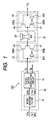
- Fig. 1 is a block diagram for showing an arrangement of a class-D amplifying apparatus 100 according to an embodiment of the present invention.
- the class-D amplifying apparatus 100 is equipped with a signal generating apparatus 10 and a driving apparatus 20.
- a data series "D Ta" is supplied from an upstream apparatus to the signal generating apparatus 10.
- the data series "D Ta” corresponds to a time sequence of Ns-bit data generated at a sampling frequency "fs”.
- the signal generating apparatus 10 generates pulse-width modulation signals "S1" and "S2" of two systems from the data series "D Ta".
- the driving apparatus 20 corresponds to a full-bridge type driving circuit which drives a load circuit 30 in a BTL (Bridge Tied Load) system based upon the pulse-width modulation signals "S1" and "S2".
- a BTL Bridge Tied Load
- the driving apparatus 20 is equipped with a driving unit 21 and another driving unit 22.
- Each of the driving units 21 and 22 is arranged by switching elements "SWa” and “SWb", and an inverter circuit "INV".
- the switching elements "SWa” and “SWb” are N-channel type field-effect transistors which have been series-connected between power supply lines.
- An output terminal of the inverter circuit INV is connected to a gate of the switching element SWb.
- the pulse-width modulation signal S1 is supplied to both a gate of the switching element SWa of the driving unit 21, and an input terminal of the inverter circuit INV of the driving circuit 21.
- the pulse width modulation signal S2 is supplied to a gate of the switching element SWa of the driving unit 22, and an input terminal of the inverter circuit INV of the driving unit 22.
- the drive current "I DR" flows through a signal path defined from the switching element "SWa” of the driving unit 22 via the load circuit 30 to the switching element "SWb" of the driving circuit 21.
- the signal generating apparatus 10 is equipped with a noise shaping filter 12 and a pulse-width modulating circuit 14.
- the noise shaping filter 12 generates a data series "D Tb" from the data series "D Ta" while the noise shaping filter 12 suppresses (namely, noise shaping) a quantize noise in an audio range.
- the above-described data series “D Tb” is a time sequence of such a data "X” whose bit number is smaller than the bit number "Ns" of each of the data contained in the data sequence "D Ta".
- a sampling frequency "fns" of the data series “D Tb" exceeds the sampling frequency "fs" of the data series "D Ta".
- the pulse-width modulating circuit 14 modulates each data "X" of the data series “D Tb" in the pulse-widthmodulationmanner so as to generate the pulse-width modulation signals "S1" and "S2".
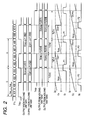
- Fig. 2 is a timing chart for explaining operations of the pulse-width modulating circuit 14. As represented in Fig. 2 , the pulse-width modulation signal "S1” is such a signal that a pulse "P1" has been arranged every unit period "T1". On the other hand, the pulse-width modulation signal "S2” is such a signal that a pulse "P2" has been arranged every unit period "T2".
- Both the unit periods “T1" and “T2” are set to a commonly-used time length (pulse period) "Tp".
- a phase difference between the pulse-width modulation signal S1 and the pulse-width modulation signal S2 is 180 degrees.
- the respective pulses "P2" of the pulse-width modulation signal S2 are positioned between the adjacent pulses "P1" which are located before and after one pulse "P2" within the pulse-width modulation signal S1.
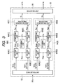
- Fig. 3 is a block diagram for exemplifying a concrete arrangement of the above-described pulse-width modulating circuit 14.
- the pulse-width modulating circuit 14 includes a converting unit 52, signal generating units "54[1]” and “54 [2]", and an adjusting unit 56.
- the respective data "X" (X[1], X[2], X[3], ---) of the data series "D Tb" are sequentially supplied from the noise shaping filter 12 every sampling period "Tns" corresponding to the sampling frequency "fns".
- the data series "D Tb” is sectioned while a set (will be referred to as “unit series” hereinafter) "U” of 4 pieces of continuous data "X” is defined as a unit, for the sake of convenience.
- the signal generating unit 54[1] of Fig. 3 generates the pulse-width modulation signal S1, and the signal generating unit 54[2] thereof generates the pulse-width modulation signal S2.
- One pulse P1 of the pulse-width modulation signal S1, and one pulse P2 of the pulse-width modulation signal S2 are defined in response to 4 pieces of data "X" (for example, X[1] to X[4]) of one unit series "U".
- the signal generating unit 54 [1] sets a time point of a front edge of the pulse P1 in response to first data "X" (X[1], X[5], ---) of the unit series "U", and also the signal generating unit 54 [1] sets a time point of a rear edge of the pulse P1 in response to second data "X" (X[2], X[6], ---) of the unit series "U).
- the signal generating unit 54[2] sets a time point of a front edge of the pulse P2 in response to third data "X" (X[3], X[7], ---) of the unit series "U", and also, the signal generating unit 54[2] sets a time point of a rear edge of the pulse P2 in response to fourth data "X" (X[4], X[8], ---) of the unit series "U".
- the converting unit 52 of Fig. 3 generates pulse definition data ("D ON1", “D OFF1”, “D ON2”, “D OFF2”) which define both the pulses “P1” and “P2" based upon 4 pieces of the data "X" within the unit series "U".
- a pulse definition data "D ONi” corresponds to data which defines a time point of a front edge (namely, rising edge) of a pulse "Pi”
- a pulse definition data "D OFFi” corresponds to data which defines a time point of a rear edge (namely, falling edge) of the pulse "Pi”.
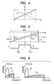
- Fig. 4 is a graph for exemplifying contents of the conversion functions "F1" and "F2". As indicated in Fig.
- the conversion function "F1" is defined as follows: That is, when the numeral value of the data "X” is a minimum value (-x), the function value “F1(X)” becomes zero, and the function value “F1(X)” is linearly increased in connection with an increase of the numeral value of the data "X”; and when the numeral value of the data “X” is amaximumvalue " (x) ", the function value "F1(X)" becomes a predetermined value "p".
- the conversion function "F2" is defined as follows: That is, when the numeral value of the data "X” is the minimum value (-x), the function value “F2 (X) " becomes the predetermined value "p", and the function value “F2(X)" is linearly decreased in connection with the increase of the numeral value of the data "X”; and when the numeral value of the data "X" is the maximum value "(x)", the function value "F2(X)" becomes zero.
- the converting unit 52 of Fig. 3 sets such a numeral value (P - F1(X[1]) to the pulse definition data "D ON1", which is obtained by subtracting a function value "F1 (X[1])" where the first data "X[1]” of the unit series “U” has been substituted for the conversion function "F1" from a predetermined value "p", and also, the converting unit 52 sets such an added value (p + F1(X[2])) to the pulse definition data "D OFF1", which is obtained by adding another function value "F1 (X[2])” where the second data "X[2]" of the unit series “U” has been substituted for the conversion function "F1" to the predetermined value "p".
- the converting unit 52 sets such a numeral value (p -F2(X[3])) to the pulse definition data "DON2", which is obtained by subtracting a function value "F2 (X[3])" where the third data "X[3]” of the unit series “U” has been substituted for the conversion function "F2" from the predetermined value "p", and also, the converting unit 52 sets such an added value (p+ F2 (X[4])) to the pulse definition data "D OFF2", which is obtained by adding another function value "F2(X[4])" where the fourth data "X[4]" of the unit series “U” has been substituted for the conversion function "F2" to the predetermined value "p".
- the pulse definition data (D ON1", “D OFF1” “D ON2”, “D OFF2”) may be sequentially generated in accordance with a similar rule with respect to other unit series “U” (for example, unit series "U” which are constituted by data X[5] to X[8]).
- the signal generating unit 54 [i] is constituted by holding units 62A[i] and 62B[i], a counting unit 64 [i], comparing units 66A[i] and 66B[i], andawaveformgeneratingunit 68 [i].
- Signals "TRGi” are supplied to the holding units 62A[i] and 62B[i].
- a signal TRG1 and another signal TRG2 correspond to such signals having time periods equal to the pulse period "TP", the phase difference of which is 180 degrees.
- the signal TRG1 falls at a starting point (endpoint) of each unit time period "T1”
- the signal TRG2 falls at a starting point (end point) of each unit time period "T2".
- the holding unit 62A[i] corresponds to a circuit (latch circuit) which holds and outputs the pulse definition data "D ONi” generated by the converting unit 52 at a falling time point of the signal "TRGi”.
- the holding unit 62B[i] corresponds to a circuit (latch circuit) which holds and outputs the pulse definition data "D OFFi” generated by the converting unit 52 at a falling time point of the signal "TRGi”.
- the counting unit 64[i] of Fig. 3 is a counter which generates a count value "Ci".
- the count value "Ci” is initialized to become zero at a starting point of a unit time period "Ti”, is linearly increased in connection with a time elapse, and then, reaches a predetermined value "2p" at an end point of the unit time period "Ti".
- the count value "Ci” represents a waveform having a saw-tooth shape, the time period of which is equal to a pulse period "TP".
- Fig. 5 is a timing chart for representing a relation between the count-value "Ci” and a pulse-width modulation signal "Si" within a single unit time period "Ti”.
- a comparing unit 66A[i] compares pulse definition data "D ONi” which is outputted from a holding unit 62A[i] with the count value "Ci” which is outputted from the counting unit 64 [i], and as shown in Fig. 5 , the comparing unit 66A[i] outputs a set signal "P SET” at a time point when the count value Ci exceeds the numeral value of the pulse definition data "D ONi".
- a comparing unit 66B[i] compares pulse definition data "D OFFi" which is outputted from a holding unit 62B[i] with the count value "Ci” which is outputted from the counting unit 64[i], and as shown in Fig. 5 , the comparing unit 66B[i] outputs a reset signal "P RES" at a time point when the count value "Ci" exceeds the numeral value of the pulse definition data "D OFF".
- the waveform generating unit 68[i] of Fig. 3 changes the signal level of the pulse-width modulation signal "Si" from a low level to a high level (namely, forms a front edge of pulse “Pi") at the time point when the set signal "P SET” is outputted from the comparing unit 66A[i], and changes the signal level of the pulse-width modulation signal "Si” from the high level to the low level (namely, forms a rear edge of pulse "Pi”) at the time point when the reset signal "P RET" is outputted from the comparing unit 66B[i].
- the pulse "Pi” has such a shape that a portion preceding from a time point (namely, center point) "tc", which divides the unit time period "Ti" by 1/2, by a time length in response to the pulse definition data "D ONi” is defined as the front edge, whereas a portion in which a time length responding to the pulse definition data "D OFFi" has elapsed from the center point "tc" is defined as a rear edge.
- the numeral values of the data X[1] and the data X[2] of the unit series “U” are maximum values (x)
- the function values F1(X[1]) and F1(X[2]) become the predetermined value "p" (refer to Fig.4 )
- the numeral value (p-F1(X[1])) of the pulse definition data "D ON1" is set to zero
- the numeral value (p + F1(X[2])) of the pulse definition data "D OFF2" is set to the predetermined value "2p".
- a duty ratio of the pulse-width modulation signal "S1" within the unit time period "T1" becomes 100 %.
- the numeral values of the data X[3] and the data X[4] of the unit series “U” are maximum values (x)
- the functionvalues F2 (X[3]) and F2 (X[4]) become zero (refer to Fig.
- both the pulse widths of the pulses "P1" and “P2” are increased, and then, the increased pulse widths are overlapped with each other.
- the adjusting unit 56 of Fig. 3 is provided to avoid the above-explained overlapping phenomenon of the pulses P1 and P2. In other words, when the pulse "P1" is overlapped with the pulse "P2", the adjusting unit 56 changes logic levels of the pulse-widthmodulation signals "S1" and "S2".
- the adjusting unit 56 maintains one of the pulses "P1" and "P2" in a high level, and further, changes the signal level of the other pulse into a low level in a forcible manner.
- the pulse-width modulation signal "S1" becomes such a signal that the pulse “P1” where two pieces of the front half data "X” within the unit series “U” have been modulated in the pulse-width modulating manner are arranged every unit time period "T1".
- the pulse-width modulation signal “S2” becomes such a signal that the pulse “P2” where two pieces of the rear half data "X” within the unit series “U” have been modulated in the pulse-width modulation manner are arranged every unit time period "T2".
- the resolution namely, stepping width of current amount of drive current "I DR"
- the pulse-width modulation signals "S1" and “S2" can be improved, as compared with that of a circuit arrangement in which a pulse width of a single pulse of a pulse-width modulation signal is controlled by one piece of data.
- the pulse period "TP” is set to such a time length equal to 4 time periods of the sampling period "Tns".
- the sampling frequency "fns” can be set to be 4 times higher than such a frequency (will be referred to as “carrier frequency” hereinafter) "fp" which corresponds to the pulse period "TP" of the pulse-width modulation signal "S1", or "S2".
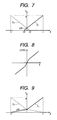
- FIG. 6 are conceptional diagrams for indicating a relation between a quantize noise "CN” and a signal component "CS", which are represented by the data series "D Tb" outputted from the noise shaping filter 12.
- the part (A) of Fig. 6 supposes such a conventional structure that the sampling frequency “fns” has been set to the same frequency as the carrier frequency "fp", whereas the part (B) of Fig. 6 supposes such a structure of the present embodiment that the sampling frequency "fn” has been set to be 4 times higher than the carrier frequency "fp". As shown in Fig.
- the relationship between the numeral values of the respective data "X" of the data series “D Tb", and the function values F1(X) and F2(X) is not limited only to the exemplified relationship of Fig. 4 .
- the conversion functions "F1" and “F2" may be alternatively defined in such a manner that when the numeral value of the data "X" becomes smaller than a predetermined value (-x0), the function value "F1(X)" becomes zero, whereas when the numeral value of the data "X" exceeds the predetermined value (x0), the function value F2(X) becomes zero.
- the signal generating apparatus 10 generates both the pulse-width modulation signals "S1" and “S2" of the two systems. Alternatively, a total number of pulse-width modulation signals “S” may be properly changed.
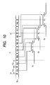
- Fig. 10 is a timing chart for explaining operations for generating pulse-width modulation signals "S1" to "S3" of 3 systems by the signal generating apparatus 10.
- a unit series “U” obtained by segmenting the data series "D Tb" contains 6 pieces of data "X" (X[1] to X[6]).
- the pule-width modulation signals "S1" and “S2" may be generated in response to the data X[1] to X[4] within the unit series "U” in a similar manner to the above-described embodiment.
- a pulse "P3" of the pulse-width modulation signal "S3” a time point of a front edge thereof is set in response to the fifth data X[5], and a time point of a rear edge thereof is set in response to the sixth data X[6] within the unit series "U".
- the sampling period "Tns" may be furthermore shortened with respect to the pulse period "TP".
Landscapes
- Engineering & Computer Science (AREA)
- Power Engineering (AREA)
- Amplifiers (AREA)
Applications Claiming Priority (1)
| Application Number | Priority Date | Filing Date | Title |
|---|---|---|---|
| JP2007276112A JP5141182B2 (ja) | 2007-10-24 | 2007-10-24 | 信号生成装置およびd級増幅装置 |
Publications (2)
| Publication Number | Publication Date |
|---|---|
| EP2056452A2 true EP2056452A2 (de) | 2009-05-06 |
| EP2056452A3 EP2056452A3 (de) | 2016-08-03 |
Family
ID=40466892
Family Applications (1)
| Application Number | Title | Priority Date | Filing Date |
|---|---|---|---|
| EP08018577.0A Withdrawn EP2056452A3 (de) | 2007-10-24 | 2008-10-23 | Signalerzeugungsvorrichtung und Klasse-D-Verstärkungsvorrichtung |
Country Status (3)
| Country | Link |
|---|---|
| US (1) | US7816981B2 (de) |
| EP (1) | EP2056452A3 (de) |
| JP (1) | JP5141182B2 (de) |
Families Citing this family (4)
| Publication number | Priority date | Publication date | Assignee | Title |
|---|---|---|---|---|
| US10388362B1 (en) * | 2018-05-08 | 2019-08-20 | Micron Technology, Inc. | Half-width, double pumped data path |
| US12003222B2 (en) * | 2021-08-13 | 2024-06-04 | Texas Instruments Incorporated | Methods and apparatus to generate a modulation protocol to output audio |
| US12034420B2 (en) | 2021-09-30 | 2024-07-09 | Texas Instruments Incorporated | Switching amplifier having linear transition totem pole modulation |
| US12562295B2 (en) | 2024-01-25 | 2026-02-24 | Texas Instruments Incorporated | Trimming resistor using modulated signal |
Citations (1)
| Publication number | Priority date | Publication date | Assignee | Title |
|---|---|---|---|---|
| JP2006054815A (ja) | 2004-08-16 | 2006-02-23 | Nagoya Institute Of Technology | デジタルパルス幅変調信号発生器 |
Family Cites Families (19)
| Publication number | Priority date | Publication date | Assignee | Title |
|---|---|---|---|---|
| US3900823A (en) * | 1973-03-28 | 1975-08-19 | Nathan O Sokal | Amplifying and processing apparatus for modulated carrier signals |
| GB9103777D0 (en) * | 1991-02-22 | 1991-04-10 | B & W Loudspeakers | Analogue and digital convertors |
| JPH0715248A (ja) * | 1993-06-22 | 1995-01-17 | Fujitsu Ten Ltd | デジタルアンプ |
| US5422597A (en) * | 1994-05-31 | 1995-06-06 | Motorola, Inc. | Means and method of enhancing signal resolution and dynamic range extension in a pulse width modulation amplifier |
| US5901176A (en) * | 1997-04-29 | 1999-05-04 | Hewlett-Packard Company | Delta-sigma pulse width modulator control circuit |
| JP2002230905A (ja) * | 2001-01-29 | 2002-08-16 | Niigata Seimitsu Kk | 音声再生装置および方法 |
| JP3896894B2 (ja) * | 2002-05-13 | 2007-03-22 | ソニー株式会社 | 電力増幅装置 |
| EP1429454A1 (de) * | 2002-12-11 | 2004-06-16 | Dialog Semiconductor GmbH | Klasse-D Verstärker mit Schwerpunktausgleichseinrichtung |
| WO2004102792A1 (en) * | 2003-05-12 | 2004-11-25 | D2Audio Corporation | Systems and methods for providing multi channel pulse width modulated audio with staggered outputs |
| JP4027276B2 (ja) * | 2003-07-09 | 2007-12-26 | シャープ株式会社 | ディジタルアンプ及びこれを用いたオーディオ再生装置 |
| JP2005079692A (ja) * | 2003-08-28 | 2005-03-24 | Renesas Technology Corp | 信号処理装置及びd級アンプ装置 |
| JP2005244595A (ja) * | 2004-02-26 | 2005-09-08 | Denon Ltd | デジタルアンプ |
| KR100604981B1 (ko) * | 2004-05-27 | 2006-07-26 | 삼성전자주식회사 | 디급 증폭기 및 펄스폭 변조 방법 |
| JP2006238293A (ja) * | 2005-02-28 | 2006-09-07 | Yamaha Corp | D級増幅器 |
| US7498876B2 (en) * | 2005-06-20 | 2009-03-03 | Agere Systems Inc. | Amplifier having half-wave tracking power rails |
| JP2007166190A (ja) * | 2005-12-13 | 2007-06-28 | Matsushita Electric Ind Co Ltd | D級アンプ |
| JP4513022B2 (ja) * | 2005-12-28 | 2010-07-28 | ソニー株式会社 | ディジタルアンプ装置及びディジタルアンプ装置のリセット方法 |
| EP1985018B1 (de) * | 2006-01-31 | 2017-11-08 | Intersil Americas LLC | Systeme und verfahren zur impulsbreitenmodulation asymmetrischer signalpegel |
| US7626519B2 (en) * | 2007-05-30 | 2009-12-01 | Texas Instruments Incorporated | Pulse-width modulation of pulse-code modulated signals at selectable or dynamically varying sample rates |
-
2007
- 2007-10-24 JP JP2007276112A patent/JP5141182B2/ja not_active Expired - Fee Related
-
2008
- 2008-10-22 US US12/288,580 patent/US7816981B2/en not_active Expired - Fee Related
- 2008-10-23 EP EP08018577.0A patent/EP2056452A3/de not_active Withdrawn
Patent Citations (1)
| Publication number | Priority date | Publication date | Assignee | Title |
|---|---|---|---|---|
| JP2006054815A (ja) | 2004-08-16 | 2006-02-23 | Nagoya Institute Of Technology | デジタルパルス幅変調信号発生器 |
Also Published As
| Publication number | Publication date |
|---|---|
| JP5141182B2 (ja) | 2013-02-13 |
| US7816981B2 (en) | 2010-10-19 |
| JP2009105703A (ja) | 2009-05-14 |
| EP2056452A3 (de) | 2016-08-03 |
| US20090108932A1 (en) | 2009-04-30 |
Similar Documents
| Publication | Publication Date | Title |
|---|---|---|
| US6693571B2 (en) | Modulation of a digital input signal using a digital signal modulator and signal splitting | |
| US8633779B2 (en) | Pulse width modulator | |
| US7920082B2 (en) | D/A converter circuit and digital input class-D amplifier | |
| US7579910B2 (en) | Low distortion switching amplifier circuits and methods | |
| JP5442636B2 (ja) | D級電力増幅器 | |
| US7948313B2 (en) | Class D amplifier circuit | |
| CN211405976U (zh) | 音频放大器和集成电路 | |
| US20030038674A1 (en) | Digital power amplifier and digital/analog converter | |
| CN109687853B (zh) | 脉冲宽度调制电路、对应的设备和方法 | |
| US7816981B2 (en) | Signal generating apparatus and class-D amplifying apparatus | |
| US6762704B1 (en) | Modulation of a digital input signal using multiple digital signal modulators | |
| JP4939752B2 (ja) | 多相インピーダンス変換増幅器 | |
| EP2163998B1 (de) | Kooperationsschaltung | |
| US7944289B2 (en) | Minimum pulse generation in a class-D amplifier | |
| US7116168B2 (en) | Power multiplier system and method | |
| US7265612B2 (en) | Low-distortion tri-state switching amplifier | |
| JPH10304657A (ja) | 電源回路 | |
| CN101729030A (zh) | D类放大器及其控制方法 | |
| US11837999B2 (en) | Audio amplifier having idle mode | |
| US7388426B2 (en) | Control circuit and method for a switching amplifier | |
| US8896376B2 (en) | Digital amplifier | |
| EP2562933A1 (de) | Verstärker der Klasse D und Steuerverfahren | |
| US20080101628A1 (en) | Switching amplifier circuits and methods | |
| US7932704B1 (en) | System and method of providing control pulses to control operation of a converter with high frequency repetitive load transients | |
| CN101820254A (zh) | 带有新型pwm电路的d类功率放大器 |
Legal Events
| Date | Code | Title | Description |
|---|---|---|---|
| PUAI | Public reference made under article 153(3) epc to a published international application that has entered the european phase |
Free format text: ORIGINAL CODE: 0009012 |
|
| AK | Designated contracting states |
Kind code of ref document: A2 Designated state(s): AT BE BG CH CY CZ DE DK EE ES FI FR GB GR HR HU IE IS IT LI LT LU LV MC MT NL NO PL PT RO SE SI SK TR |
|
| AX | Request for extension of the european patent |
Extension state: AL BA MK RS |
|
| PUAL | Search report despatched |
Free format text: ORIGINAL CODE: 0009013 |
|
| AK | Designated contracting states |
Kind code of ref document: A3 Designated state(s): AT BE BG CH CY CZ DE DK EE ES FI FR GB GR HR HU IE IS IT LI LT LU LV MC MT NL NO PL PT RO SE SI SK TR |
|
| AX | Request for extension of the european patent |
Extension state: AL BA MK RS |
|
| RIC1 | Information provided on ipc code assigned before grant |
Ipc: H03F 3/217 20060101AFI20160627BHEP |
|
| AKY | No designation fees paid | ||
| AXX | Extension fees paid |
Extension state: BA Extension state: RS Extension state: MK Extension state: AL |
|
| REG | Reference to a national code |
Ref country code: DE Ref legal event code: R108 |
|
| STAA | Information on the status of an ep patent application or granted ep patent |
Free format text: STATUS: THE APPLICATION IS DEEMED TO BE WITHDRAWN |
|
| 18D | Application deemed to be withdrawn |
Effective date: 20170204 |