EP2060932B1 - Détecteur de rayons gamma - Google Patents
Détecteur de rayons gamma Download PDFInfo
- Publication number
- EP2060932B1 EP2060932B1 EP07792245.8A EP07792245A EP2060932B1 EP 2060932 B1 EP2060932 B1 EP 2060932B1 EP 07792245 A EP07792245 A EP 07792245A EP 2060932 B1 EP2060932 B1 EP 2060932B1
- Authority
- EP
- European Patent Office
- Prior art keywords
- gamma ray
- detecting element
- gamma
- stage
- energy
- Prior art date
- Legal status (The legal status is an assumption and is not a legal conclusion. Google has not performed a legal analysis and makes no representation as to the accuracy of the status listed.)
- Ceased
Links
Images





Classifications
-
- G—PHYSICS
- G01—MEASURING; TESTING
- G01T—MEASUREMENT OF NUCLEAR OR X-RADIATION
- G01T1/00—Measuring X-radiation, gamma radiation, corpuscular radiation, or cosmic radiation
- G01T1/16—Measuring radiation intensity
- G01T1/24—Measuring radiation intensity with semiconductor detectors
- G01T1/242—Stacked detectors, e.g. for depth information
Definitions
- the present invention relates to a gamma ray detector, and more particularly to a gamma ray detector that can detect an arrival direction of gamma rays.
- a gamma ray detector that utilizes the kinematics of Compton scattering is disclosed in JP Patent Publication (Kokai) No. 9-101371 A (1997 ) or JP Patent Publication (Kokai) No. 2005-208057 A as a gamma ray detector that can detect the position of a gamma-ray source or an arrival direction of gamma rays without using a collimator.
- the aforementioned gamma ray detector uses two germanium detecting elements that have a position resolution and an energy resolution, and focuses on a gamma ray detection event in which a gamma ray incident on a front germanium detecting element undergoes Compton scattering, and thereafter the scattered gamma rays are incident and absorbed by a rear germanium detecting element to thereby calculate a position or a direction in which a gamma-ray source exists based on the detected positions and detected energy of the gamma ray at the two germanium detecting elements.
- an image pickup apparatus for gamma-ray astronomy is described that applies the same principle by combining a silicon detecting element and a cadmium telluride (CdTe) detecting element.
- a gamma ray detector that uses two germanium detecting elements is capable of detecting gamma rays over a wide energy range.
- the probability of photoelectric absorption occurring in a germanium crystal increases, and the sensitivity of gamma ray detection utilizing Compton scattering decreases.
- Figure 1 is a view that illustrates the relationship between the probability of Compton scattering occurring and germanium thickness, taking gamma ray energy as a parameter.
- the probability of Compton scattering occurring remains at approximately 20% irrespective of how thick the germanium crystal is made, and the detection efficiency drops remarkably.
- An object of the present invention is to provide a gamma ray detector that increases a detectable energy range.
- the gamma ray detector comprises a configuration comprising a first-stage detecting element, a second-stage detecting element and a third-stage detecting element that are aligned in parallel in that order from a side, from which gamma rays are incident, each of the second-stage detecting element and the third-stage detecting element being a position-sensitive gamma ray detecting element for high energy gamma rays adapted to detect an interaction position and an energy of a gamma ray; and the first-stage detecting element being a position-sensitive gamma ray detecting element for low energy gamma rays adapted to detect an interaction position and an energy of a gamma ray, wherein the gamma ray detector is adapted to detect a gamma ray that
- Compton scattering of low-energy gamma rays occurs mainly at the silicon detecting element, and scattered gamma rays are detected with the germanium detecting elements to the rear thereof. Further, since high-energy gamma rays tend to pass through the silicon detecting element, high-energy gamma rays undergo Compton scattering mainly at the germanium detecting element at the next stage, and the scattered gamma rays are detected with a rearmost detecting element. Accordingly, it is possible to pick-up images of low-energy to high-energy gamma rays with a high efficiency. As a result, SPECT nuclear imaging for in vivo diagnosis that discharges low-energy gamma rays which has heretofore been difficult to perform with a gamma-ray image pickup apparatus using two germanium detecting elements is also enabled.
- Figure 2 is a view that illustrates the relationship between the probability of Compton scattering occurring and crystal thickness with respect to germanium crystals and silicon crystals.
- silicon as a raw material for a detecting element at the first stage, the probability of Compton scattering occurring can be improved even for a gamma ray with energy of approximately 100 keV. Accordingly, use of silicon for a first-stage detecting element and use of germanium or CdTe for a second-stage detecting element can be considered.
- a configuration is employed in which a gamma ray detecting element (hereunder, referred to as “gamma ray detecting element for low energy") that exhibits a high Compton scattering occurrence probability with respect to relatively low energy gamma rays is disposed in front of two gamma ray detecting elements (hereunder, referred to as "gamma ray detecting element for high energy”) that exhibit a high Compton scattering occurrence probability with respect to relatively high energy gamma rays.
- gamma ray detecting element for low energy a gamma ray detecting element that exhibits a high Compton scattering occurrence probability with respect to relatively low energy gamma rays.
- the gamma ray detector of the present invention comprises a pair of position-sensitive gamma ray detecting elements for high-energy gamma rays that can detect an interaction position and an energy of a gamma ray, and a position-sensitive gamma ray detecting element for low-energy gamma rays that can detect an interaction position and an energy of a gamma ray and which is disposed in front of the pair of position-sensitive gamma ray detecting elements for high-energy gamma rays.
- the position-sensitive gamma ray detecting elements for high-energy gamma rays comprise germanium crystals
- the position-sensitive gamma ray detecting element for low energy gamma rays comprises silicon crystals.
- the position-sensitive gamma ray detecting element for low-energy gamma rays is a detecting element that typically results in a higher Compton scattering occurrence probability with respect to gamma rays of energy 100 keV, compared to the position-sensitive gamma ray detecting elements for high-energy gamma rays, and results in a lower Compton scattering occurrence probability with respect to gamma rays of energy 1000 keV compared to the position-sensitive gamma ray detecting elements for high-energy gamma rays
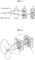
- FIG 3 is a schematic diagram that illustrates the disposition of gamma ray detecting elements in a gamma ray detector according to the present invention.
- the gamma ray detector according to the present invention has a configuration in which a first-stage detecting element 101, a second-stage detecting element 102, and a third-stage detecting element 103 are aligned in parallel in that order from a side from which gamma rays are incident.
- the first-stage detecting element 101 is a gamma ray detecting element for low energy that comprises a silicon semiconductor detecting element.
- the second-stage detecting element 102 and the third-stage detecting element 103 are each a gamma ray detecting element for high energy that comprise a germanium semiconductor detecting element. Diamond may also be used as the material of the first-stage detecting element 101. Further, the third-stage detecting element 103 can be substituted with a CdTe detecting element or a CdZnTe detecting element with a larger atomic number or the like.
- Each gamma ray detecting element is a position-sensitive semiconductor detecting element that is capable of measuring the position of a point of interaction with a gamma ray as well as an energy imparted to the detecting element by the interaction according to the principle described hereunder.
- a high-energy gamma ray of approximately 200 keV or more that is discharged from the gamma-ray source tends to pass through the first-stage silicon detecting element to undergo Compton scattering mainly at the second-stage germanium detecting element. If it is assumed that the scattered gamma ray undergoes photoelectric absorption at the third-stage detecting element, then, similarly to the case of the low energy gamma ray, an opening angle cone that is double the scattering angle is defined that takes a straight line that passes through two measured interaction points as an axis and takes the interaction point in the second-stage detecting element as the vertex. More specifically, it is possible to perform highly efficient imaging of low-energy to high-energy gamma rays by the Compton camera method.
- the first-stage detecting element 101 or the second-stage detecting element 102 may be the scattering detector.
- the second-stage detecting element 102 and the third-stage detecting element 103 may be an absorption detector. Further, in a case in which the second-stage detecting element 102 is the scattering detector, the third-stage detecting element 103 may be the absorption detector.
- Figure 4 is a view that illustrates the principle for detecting a gamma-ray source by means of a scattering detector and an absorption detector.
- the scattered gamma rays are incident on an absorption detector 12 and lose all energy there.
- the present invention focuses on this event.
- the gamma ray 14 imparts an energy of E 1 to the scattering detector 11 at the front, and imparts an energy of E 2 to the absorption detector 12 at the rear.
- E E 1 + E 2
- the Compton scattering angle ⁇ is calculated based on the kinematics of Compton scattering according to the following formula (2).
- m c is the rest mass of an electron
- c is optical velocity.
- the gamma-ray source 13 can be found on a circular cone whose vertex angle is 20 with respect to a straight line that connects an interaction point at which the gamma ray 14 caused Compton scattering in the scattering detector 11 and an interaction point at which the scattered gamma ray is absorbed by the absorption detector 12. Accordingly, two or more sets of such events are measured, and circular cones are formed for each combination. When a position at which these circular cones overlap is determined, the position is a candidate for the position at which the gamma-ray source 13 exists. As the measured number of events, i.e. the number of circular cones, increases, an area in which the circular cones overlap with each other can be narrowed and the position at which a gamma-ray source exists can be determined with high accuracy.
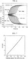
- Figure 5 is a view for illustrating construction examples of individual gamma ray detecting elements, in which (a) is a top view, (b) is a front view, and (c) is a side view.
- a gamma ray detecting element that can be used with the present invention is not limited to the detecting elements having the structures shown in Figure 5 , and any kind of detecting element can be used as long as the detecting element is a gamma ray detecting element that can detect an interaction position and an energy with respect to a gamma ray.
- This detecting element forms an electrode that is divided in a rectangular shape on both surfaces of a planar gamma-ray detector crystal 20 with dimensions a ⁇ b ⁇ c.
- Multiple electrode strips 21 of width d and length a that are elongated in the X direction are tightly aligned on one surface of the planar gamma-ray detector crystal 20.
- multiple electrode strips 22 of width d and length b that are elongated in the Y direction are tightly aligned on the surface on the opposite side of the planar gamma-ray detector crystal 20.
- the electrode strips on the one surface are used as anodes (hereinafter referred to as "anode strip”), and the electrode strips on the surface on the opposite side are used as cathodes (hereinafter referred to as “cathode strip”).
- the multiple anode strips 21 and cathode strips 22 that extend in mutually intersecting directions in this manner are respectively provided on the front and rear surfaces of the planar gamma-ray detector crystal 20.
- Rough X-Y coordinates of an interaction point are known from a combination of the anode strips and cathode strips in which a signal caused by interaction between a gamma ray and a gamma-ray detector crystal is detected strongly.
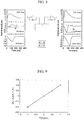
- Figure 6 is a view for simulating an output signal generated from anode strips and cathode strips when a gamma ray interacts with a gamma-ray detector crystal inside a divided-electrode-type planar gamma ray detecting element.
- the illustrated signal is a signal that is generated from the anode strips and cathode strips nearest to an interaction point.
- the signal waveform changes according to a DOI (Depth of interaction) position in the depth direction of the interaction point of the gamma ray.
- DOI Depth of interaction
- Figure 7 illustrates the relationship between a difference in the time until the amplitude of a signal waveform detected by the anode strip 21 reaches 50% of the maximum value and the time until the amplitude of the signal waveform detected by the cathode strip 22 reaches 50% of the maximum value, and DOI with regard to a single detection event. It is found that this time difference and the DOI have an almost linear relationship. Accordingly, when the relationship shown in Figure 7 is stored, and when the measured time difference is applied to the relationship of Figure 7 , the DOI, that is, the depth from the surface of a gamma-ray detector crystal at an interaction point can be known.
- the X-Y coordinates of the interaction point can be known from the position of the anode strip that exhibits the maximum signal amplitude among the multiple anode strips and the position of the cathode strip that exhibits the maximum signal amplitude among the multiple cathode strips.
- the electrode strip has width d
- the X-Y coordinates of the interaction point are determined with an accuracy that is smaller than the width of the electrode strip according to the method described below.
- Figure 8 is a view that describes a method of measuring with high accuracy the crosswise position of an interaction point between a gamma-ray detector crystal and a gamma ray, that is, the position within the width of an electrode strip.
- a signal is detected from multiple anode strips provided on the front surface of the detecting element, and the signal generated from the anode strip nearest to the interaction point exhibits the maximum amplitude.
- a signal is also detected from multiple cathode strips provided on the rear surface of the detector, and the signal generated from the cathode strip nearest to the interaction point exhibits the maximum amplitude.
- Figure 8 is a view that shows signal waveforms detected by the electrode strips on the two sides adjacent to the electrode strip that exhibits the maximum signal amplitude.
- the graph on the left side in Figure 8 shows the signal waveform of the electrode strip on the immediate left of the electrode strip that exhibits the maximum signal amplitude
- the graph on the right side shows the signal waveform of the electrode strip on the immediate right of the electrode strip that exhibits the maximum signal amplitude.
- TOIs transverse positions of interaction
- Figure 9 is a view that illustrates the relationship between TOI and the parameter L defined by the above formula (3). As illustrated, the TOI and the parameter L have an almost linear relationship. Accordingly, when the relationship shown in Figure 9 is stored, and the parameter L that is calculated based on the amplitudes A + and A - measured based on the signal waveforms of the adjacent electrode strips on both sides of an electrode strip that exhibits the maximum signal amplitude is applied to the relationship shown in Figure 9 , the TOI, that is, the position of the interaction point of a gamma ray within the width d of the electrode can be known with high accuracy.
- the Y coordinate position of the interaction point can be obtained with high accuracy.
- the X coordinate position of the interaction point can be obtained with high accuracy.
- Whether a strip is nearest to an interaction point or is a strip adjacent to the nearest strip can be identified using a difference in the signal waveform obtained from those strips.
- a wave height is ⁇ 100 at 500 ns in Figure 6
- the wave height is 0 at 300 ns in Figure 8 . Accordingly, when a wave discriminator for identifying a difference in this waveform is manufactured and applied, both the nearest strip and the adjacent strips can be identified, and it then known whether a strip is a strip (DOI strip) for detecting DOI or a strip (TOI strip) for detecting TOI.
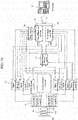
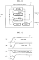
- FIG. 10 is a schematic block diagram that illustrates an example of a signal processing section of a gamma-ray image pickup apparatus according to the present invention.
- First-stage, second-stage and third-stage detecting elements 101, 102, and 103 of the detection section 10 are secured to a copper cold finger cooled with liquid nitrogen inside a liquid nitrogen container, and cooled. Signals from the multiple anode strips and multiple cathode strips provided in the first-stage detecting element 101 are amplified by respective preamplifiers.
- signals from the multiple anode strips and multiple cathode strips provided in the second-stage detecting element 102, and signals from the multiple anode strips and multiple cathode strips provided in the third-stage detecting element 103 are also amplified by respective preamplifiers.
- the preamplifiers that are connected to the cathode strips and anode strips of the first-stage detecting element 101 are represented by a preamplifier 1 and a preamplifier 3, respectively
- the preamplifiers that are connected to the cathode strips and anode strips of the second-stage detecting element 102 are represented by a preamplifier 2 and a preamplifier 4, respectively
- the preamplifiers that are connected to the cathode strips and anode strips of the third-stage detecting element 103 are represented by a preamplifier 5 and a preamplifier 6, respectively.
- the output signal of each preamplifier is input to a signal processing circuit 32 that is shown in detail in Figure 11 .
- the signal processing circuit 32 When an input signal belongs to a DOI strip, the signal processing circuit 32 outputs an energy signal to output A and outputs a time signal to output T.
- the signal of the output A is utilized for TOI measurement, and no signal is output to the output T.
- the signal input to the signal processing circuit 32 is divided into four signals, and input to a waveform discriminator 41, an amplitude measuring device 42, a shaping amplifier 43, and a TFA 44, respectively.
- a preamplifier 31 used here is called a "charge-sensitive preamplifier", and outputs a signal having the wave height that is proportional to an amount of charge generated in a detecting element by interaction with a gamma ray.
- the waveform discriminator 41 is set so that a gate signal is output when the output waveform of the preamplifier 31 maintains a specific wave height even after 300 ns after a certain threshold is exceeded, and so that no signal is output when the preamplifier 31 does not maintain a specific wave height.
- the amplitude measuring device 42 is a circuit for outputting the difference between the maximum value and the minimum value of the output of the preamplifier 31.
- the shaping amplifier 43 generates a semi-Gaussian waveform to output a signal having a wave height that is proportional to the wave height of the preamplifier 31 with excellent accuracy.
- This circuit is realized by connecting an RC integrated circuit in multiple stages behind a CR differentiation circuit.
- the TFA (timing filter amplifier) 44 forms a bandpass circuit. In this case, a lowpass time constant is 50 ns, and a high-pass time constant is 500 ns.
- a CFD 45 is a commercially available circuit called a constant fraction discriminator, and the operating principle thereof will now be described with reference to Figure 12 .
- An input signal 51 shown in (a) is divided into two signals to create a signal 52, as shown in (b), for which the input signal 51 is delayed by t d , and a signal 53, as shown in (c), for which the input signal 51 is inverted and whose amplitude is multiplied by f.
- a time t r at which the wave height thereof is 0 is a time obtained by adding t d to the time taken for the wave height of the input signal 51 to reach the maximum value multiplied by f.
- the time taken to reach the maximum value of the wave height multiplied by f can be known by making a signal of a rising waveform or a falling waveform pass through the CDF.
- a coincidence detection circuit 33 is a circuit that outputs a gate signal when the time difference of an input signal is shorter than a setting value. The width and delay time of the gate signal are variable. The coincidence detection circuit 33 selects an event in which gamma ray interaction is detected with only any two among the three detecting elements 101, 102, and 103, and acquires data.
- a time difference recorder 35 is a circuit that records a time difference between a start signal and a stop signal using the gate signal output of the coincidence detection circuit 33 as the start signal, and using the signal in which the output T of the signal processing circuit 32 is delayed through a delay circuit 34 as the stop signal.
- a wave height recorder 36 is a circuit that records the maximum value of the wave height of the signal for the output A of the signal processing circuit 32 while the gate signal of the coincidence detection circuit 33 is being output.
- the waveform discriminator 41 checks whether or not an input signal belongs to a DOI strip.
- a gate signal is output, and the output signal of the amplitude measuring device 42 is not output.
- a configuration is adopted such that the output signals of the shaping amplifier 43 and the CFD 44 can be output.
- a gate signal is not output, output of the output signal of the amplitude measuring device 42 is enabled, and output of output signals of the shaping amplifier 43 and CFD 44 is disabled.
- the amplitude measuring device 42 measures and outputs the difference between the maximum value and the minimum value of the input signal.
- the shaping amplifier 43 generates a signal of a waveform suitable to energy measurement.
- the TFA 44 generates a signal of a waveform suitable to time measurement. The output of the TFA 44 is input to the CFD 45, and an output signal is generated when 50% of the maximum value of the wave height is reached.
- the output T of the signal processing circuit 32 is only output with respect to a signal of a DOI strip. That is, data is created only in a channel that corresponds to the DOI strip, of the time difference recorder 35. Further, among the data of the wave height recorder 36, the data that corresponds to that channel and the data of the adjacent channels on both sides of that channel are transferred by data transfer processing. The data of the time difference recorder 35 and the wave height recorder 36 is transferred to a computer 37 for each measurement event, and processing for image generation is executed. Figure 13 shows the details of the data that is transferred.
- reference characters t 1 to t 4 denote data of the time difference recorder 35.
- Reference characters t 1 and t 3 denote data of cathode strips and anode strips of a scattering detector
- reference characters t 2 and t 4 denote data of cathode strips and anode strips of an absorption detector.
- ID information for identifying a channel and a numerical value obtained from the relevant channel are recorded as a set.
- Reference characters E 1 and thereafter denote data of the wave height recorder 36.
- Reference characters E 1 and E 3 denote data obtained for the DOI strips of the cathode and anode, respectively, of the scattering detector.
- Reference characters E 2 and E 4 denote data obtained for the DOI strips of the cathode and anode, respectively, of the absorption detector.
- Reference characters A 1+ and A 1- denote data obtained for adjacent strips (TOI strips) on both sides of the DOI strip of the cathode of the scattering detector.
- Reference characters A 2+ and A 2- denote data obtained for adjacent strips (TOI strips) on both sides of the DOI strip of the cathode of the absorption detector.
- Reference characters A 3+ and A 3- denote data obtained for adjacent strips (TOI strips) on both sides of the DOI strip of the anode of the scattering detector.
- Reference characters A 4+ and A 4- denote data obtained for adjacent strips (TOI strips) on both sides of the DOI strip of the anode of the absorption detector.
- Figure 14 shows a flow of data processing by the computer 37. This processing is repeated for the number of detection events.
- a detection pattern is checked in step 12.
- the detection pattern is checked based on the data of the time difference recorder 35.
- data exists in a certain channel of the time difference recorder 35, it indicates that the strip that is the source of the data is a DOI strip.
- the processing advances to the next step only in a case in which only one strip, respectively, among the strips of the respective anodes and cathodes of the scattering detector and absorption detector is a DOI strip.
- step 13 When there are two or more DOI strip signals, such as in a case in which two gamma rays are incident on a detecting element at the same time, the event is excluded from subsequent analyzing.
- the energy is checked in step 13. This energy check is performed using the E 1 and E 2 of the wave height recorder 36.
- the processing advances to the next step only when the sum of E 1 and E 2 is equal to the energy of the gamma ray of interest.
- the DOI computation of step 14 is performed using the data of the time difference recorder 35.
- the DOI in the scattering detector is calculated from the difference between t 1 and t 3
- the DOI in the absorption detector is calculated from the difference between t 2 and t 4 .
- the TOI computation of the subsequent step 15 is performed using the data of the wave height recorder 36.
- the dividing direction of the cathode is the X-axis direction
- the dividing direction of the anode is the Y-axis direction.
- the TOI in the X-axis direction of the scattering detector is calculated based on A 1+ and A 1-
- the TOI in the Y-axis direction of the scattering detector is calculated based on A 3+ and A 3-
- the TOI in the X-axis direction of the absorption detector is calculated based on A 2+ and A 2-
- the TOI in the Y-axis direction of the absorption detector is calculated based on A 4+ and A 4- .
- step 16 calculates a Compton scattering angle ⁇ by applying the energy E 1 detected at the scattering detector and the energy E 2 detected at the absorption detector to the above formula (2).
- low-energy gamma rays undergo Compton scattering mainly at a silicon detecting element, and the scattered gamma rays are detected at a germanium detecting element provided to the rear of the silicon detecting element.
- the high-energy gamma rays can be detected by two germanium detecting element in the conventional manner. It is therefore possible to detect with high efficiency gamma rays extending over a range from low-energy gamma rays of approximately 100 keV to high-energy gamma rays of approximately 2 MeV.
- Figure 15(a) is a view that illustrates the combination of detecting elements employed in the gamma ray detector of the present invention.
- the first-stage detecting element comprises silicon of a thickness of 10 mm
- the second-stage detecting element comprises germanium of a thickness of 10 mm
- the third-stage detecting element comprises germanium of a thickness of 20 mm.
- Figure 15(b) is a view that illustrates a gamma ray detector as a comparison example, in which the first-stage detecting element comprises silicon of a thickness of 10 mm and the second-stage detecting element comprises germanium of a thickness of 20 mm.
- Figure 15(c) is also a view that illustrates a gamma ray detector as a comparison example, in which the first-stage detecting element comprises germanium of a thickness of 10 mm and the second-stage detecting element comprises germanium of a thickness of 20 mm.
- the dimensions of the detecting elements are 39 mm x 39 mm for length x height, a space between each detecting element is 30 mm, and a gamma-ray source is located 30 mm to the front of the first-stage detecting element.
- the detector of the present invention achieves a detection efficiency that is more than twice that of the detector with the Si+Ge combination.
- an apparatus capable of picking up images of gamma rays of an energy range from approximately 100 keV to 2 MeV with a high resolution and high efficiency can be realized by the Compton camera method.
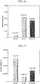
- Figure 18 is a view that illustrates the frequency at which interactions occur with the respective detecting element combinations when picking up images with the gamma ray detector according to the present invention.
- reference characters Gel+Ge2, Si+Ge2, and Si+Ge1 denote a combination of the second-stage and third-stage detecting elements, a combination of the first-stage and third-stage detecting elements, and a combination of the first-stage and second-stage detecting elements, respectively.
- the energy is 100 keV
- 94.28% of interactions occur in Si+Ge1
- the contribution of the third-stage detecting element is small.
Landscapes
- Physics & Mathematics (AREA)
- Health & Medical Sciences (AREA)
- Life Sciences & Earth Sciences (AREA)
- General Physics & Mathematics (AREA)
- High Energy & Nuclear Physics (AREA)
- Molecular Biology (AREA)
- Spectroscopy & Molecular Physics (AREA)
- Measurement Of Radiation (AREA)
- Nuclear Medicine (AREA)
Claims (4)
- Détecteur de rayons gamma comprenant :une configuration comprenant un élément de détection de premier niveau (101), un élément de détection de deuxième niveau (102) et un élément de détection de troisième niveau (103) qui sont alignés parallèlement dans cet ordre à partir d'un côté à partir duquel des rayons gamma (14, 15) sont incidents, chacun des éléments de détection de deuxième niveau (102) et de troisième niveau (103) étant un élément de détection de rayons gamma sensible à la position pour les rayons gamma de haute énergie, adaptés pour détecter une position d'interaction et une énergie d'un rayon gamma ; etl'élément de détection de premier niveau (101) étant un élément de détection de rayons gamma sensible à la position pour les rayons gamma de basse énergie adapté pour détecter une position d'interaction et une énergie d'un rayon gamma,le détecteur de rayons gamma étant adapté pour détecter un rayon gamma qui est absorbé photoélectriquement et détecté par l'élément de détection de deuxième niveau (102) après avoir subi une diffusion Compton et avoir été détecté par l'élément de détection de premier niveau (101), le détecteur de rayons gamma étant en outre adapté pour détecter un rayon gamma qui est absorbé photoélectriquement et détecté par l'élément de détection de troisième niveau (103) après avoir subi une diffusion Compton et avoir été détecté par l'élément de premier niveau (101), et le détecteur de rayons gamma étant en outre adapté pour détecter un rayon gamma qui est absorbé photoélectriquement et détecté par l'élément de détection de troisième niveau (103) après avoir subi une diffusion Compton et avoir été détecté par l'élément de deuxième niveau (102).
- Détecteur de rayons gamma selon la revendication 1, caractérisé en ce que les éléments de détection de rayons gamma sensibles à la position (102, 103) pour les rayons gamma de haute énergie comprennent chacun un cristal de germanium, comme cristal planaire détectant les rayons gamma, et l'élément de détection de rayons gamma sensible à la position (101) pour les rayons gamma de basse énergie comprend un cristal de silicium, comme cristal planaire détectant les rayons gamma.
- Détecteur de rayons gamma selon la revendication 1 ou 2, comprenant en outre un circuit de détection en coïncidence (33) adapté pour extraire uniquement les événements dans lesquels l'interaction d'un rayon gamma est détectée dans uniquement deux des trois éléments de détection de rayons gamma sensibles à la position (101, 102, 103).
- Détecteur de rayons gamma selon la revendication 3, caractérisé en ce que l'épaisseur de l'élément de détection de deuxième niveau (102) est de 10 mm et l'épaisseur de l'élément de détection de troisième niveau (103) est de 20 mm.
Applications Claiming Priority (2)
| Application Number | Priority Date | Filing Date | Title |
|---|---|---|---|
| JP2006220446A JP4486623B2 (ja) | 2006-08-11 | 2006-08-11 | コンプトン撮像カメラ |
| PCT/JP2007/065593 WO2008018534A1 (fr) | 2006-08-11 | 2007-08-09 | détecteur de rayons gamma |
Publications (3)
| Publication Number | Publication Date |
|---|---|
| EP2060932A1 EP2060932A1 (fr) | 2009-05-20 |
| EP2060932A4 EP2060932A4 (fr) | 2014-02-12 |
| EP2060932B1 true EP2060932B1 (fr) | 2017-03-08 |
Family
ID=39033063
Family Applications (1)
| Application Number | Title | Priority Date | Filing Date |
|---|---|---|---|
| EP07792245.8A Ceased EP2060932B1 (fr) | 2006-08-11 | 2007-08-09 | Détecteur de rayons gamma |
Country Status (4)
| Country | Link |
|---|---|
| US (1) | US8076645B2 (fr) |
| EP (1) | EP2060932B1 (fr) |
| JP (1) | JP4486623B2 (fr) |
| WO (1) | WO2008018534A1 (fr) |
Cited By (4)
| Publication number | Priority date | Publication date | Assignee | Title |
|---|---|---|---|---|
| US11426135B2 (en) | 2018-08-07 | 2022-08-30 | Siemens Medical Solutions Usa, Inc. | Multi-modal Compton and single photon emission computed tomography medical imaging system |
| US11701074B2 (en) | 2018-08-07 | 2023-07-18 | Siemens Medical Solutions Usa, Inc. | Compton camera with segmented detection modules |
| US11744528B2 (en) | 2018-08-07 | 2023-09-05 | Siemens Medical Solutions Usa, Inc. | Adaptive Compton camera for medical imaging |
| US12048571B2 (en) | 2018-08-07 | 2024-07-30 | Siemens Medical Solutions Usa, Inc. | Near 2Pi Compton camera for medical imaging |
Families Citing this family (21)
| Publication number | Priority date | Publication date | Assignee | Title |
|---|---|---|---|---|
| JP5697982B2 (ja) | 2007-09-07 | 2015-04-08 | コーニンクレッカ フィリップス エヌ ヴェ | 複数の変換層を持つ放射線検出器、x線検出器および画像形成システム |
| JP5446011B2 (ja) * | 2008-06-25 | 2014-03-19 | 独立行政法人放射線医学総合研究所 | ガンマ線検出器、放射線診断装置、断層像撮影装置、その解析方法、コンピュータプログラム及び記憶媒体 |
| WO2009157071A1 (fr) * | 2008-06-25 | 2009-12-30 | 独立行政法人放射線医学総合研究所 | Détecteur de rayons gamma, analyseur de rayonnement, appareil d'imagerie en coupe transversale et son procédé d'analyse |
| JP5467839B2 (ja) * | 2009-10-13 | 2014-04-09 | 日立アロカメディカル株式会社 | 放射線測定装置 |
| JP5395753B2 (ja) * | 2010-06-22 | 2014-01-22 | 株式会社日立製作所 | 放射線計測装置 |
| US8710450B2 (en) * | 2010-11-03 | 2014-04-29 | University Of New Hampshire | Tri-material dual-species neutron spectrometer |
| US9507035B2 (en) | 2010-11-03 | 2016-11-29 | University Of New Hampshire | Tri-material dual-species neutron/gamma spectrometer |
| JP5526435B2 (ja) * | 2011-08-03 | 2014-06-18 | 独立行政法人理化学研究所 | Pet装置およびそのイメージング方法 |
| FR2997766B1 (fr) * | 2012-11-08 | 2015-06-12 | Alain Iltis | Systeme et procede de detection de rayonnement gamma de type gamma camera |
| JP5840638B2 (ja) | 2013-03-21 | 2016-01-06 | 株式会社東芝 | 放射線検出装置及び放射線の検出方法 |
| DE102013219821A1 (de) * | 2013-09-30 | 2015-04-02 | Fraunhofer-Gesellschaft zur Förderung der angewandten Forschung e.V. | Röntgendetektor |
| CN104111470A (zh) * | 2014-07-15 | 2014-10-22 | 清华大学 | 半导体探测器的信号处理方法及装置 |
| JP6550699B2 (ja) | 2014-08-04 | 2019-07-31 | 三菱重工業株式会社 | コンプトンカメラ用検出器及びコンプトンカメラ |
| EP3190431B1 (fr) | 2014-09-05 | 2019-03-20 | Riken | Dispositif et procédé d'imagerie |
| JP6781918B2 (ja) * | 2016-09-02 | 2020-11-11 | 国立大学法人群馬大学 | 情報処理装置、イメージング方法、及び、イメージングプログラム |
| EP3306353A1 (fr) * | 2016-10-07 | 2018-04-11 | Danmarks Tekniske Universitet | Détecteur de radiations |
| US10768320B2 (en) | 2017-05-11 | 2020-09-08 | University Of New Hampshire | Field deployable neutron/gamma spectrometer |
| EP3764128B1 (fr) * | 2018-04-09 | 2024-09-18 | University Public Corporation Osaka | Dispositif et procédé de détection de rayonnements électromagnétiques |
| JP7014423B2 (ja) * | 2018-09-21 | 2022-02-01 | 学校法人北里研究所 | 放射線検出装置、放射線検出方法およびプログラム |
| CN109725342A (zh) * | 2019-01-01 | 2019-05-07 | 中国人民解放军63653部队 | 一种用于现场低能γ射线测量的散射抑制探测结构 |
| US11701065B2 (en) * | 2019-05-22 | 2023-07-18 | Redlen Technologies, Inc. | Compton scattering correction methods for pixellated radiation detector arrays |
Family Cites Families (11)
| Publication number | Priority date | Publication date | Assignee | Title |
|---|---|---|---|---|
| JPS62203078A (ja) * | 1986-02-28 | 1987-09-07 | Shimadzu Corp | 放射線位置検出器 |
| US5175434A (en) * | 1991-07-01 | 1992-12-29 | Sopha Medical Systems, Inc. | Compton scatter camera |
| US5567944A (en) * | 1995-04-28 | 1996-10-22 | University Of Cincinnati | Compton camera for in vivo medical imaging of radiopharmaceuticals |
| JPH09101371A (ja) | 1995-10-06 | 1997-04-15 | Rikagaku Kenkyusho | ガンマ線検出方法及び検出装置 |
| WO1998052069A1 (fr) * | 1997-05-16 | 1998-11-19 | University Of Michigan | Procede d'amelioration de la resolution spatiale d'une camera compton |
| US5841141A (en) * | 1997-06-03 | 1998-11-24 | The University Of Utah | Image reconstruction from V-projections acquired by Compton camera |
| US6528795B2 (en) * | 2000-04-27 | 2003-03-04 | The United States Of America As Represented By The Secretary Of The Navy | Compton scatter imaging instrument |
| JP3976259B2 (ja) * | 2002-10-07 | 2007-09-12 | 株式会社日立製作所 | ポジトロンエミッショントモグラフィ装置 |
| US6881959B2 (en) * | 2002-10-31 | 2005-04-19 | The Regents Of The University Of Michigan | Method and system for generating an image of the radiation density of a source of photons located in an object |
| JP2005208057A (ja) | 2003-12-26 | 2005-08-04 | Institute Of Physical & Chemical Research | ガンマ線検出器及びガンマ線撮像装置 |
| EP1548465A1 (fr) * | 2003-12-26 | 2005-06-29 | Riken | Détecteur de rayonnement gamma et dispositif de prise d'images |
-
2006
- 2006-08-11 JP JP2006220446A patent/JP4486623B2/ja not_active Expired - Fee Related
-
2007
- 2007-08-09 EP EP07792245.8A patent/EP2060932B1/fr not_active Ceased
- 2007-08-09 US US12/377,250 patent/US8076645B2/en not_active Expired - Fee Related
- 2007-08-09 WO PCT/JP2007/065593 patent/WO2008018534A1/fr not_active Ceased
Non-Patent Citations (1)
| Title |
|---|
| None * |
Cited By (6)
| Publication number | Priority date | Publication date | Assignee | Title |
|---|---|---|---|---|
| US11426135B2 (en) | 2018-08-07 | 2022-08-30 | Siemens Medical Solutions Usa, Inc. | Multi-modal Compton and single photon emission computed tomography medical imaging system |
| US11701074B2 (en) | 2018-08-07 | 2023-07-18 | Siemens Medical Solutions Usa, Inc. | Compton camera with segmented detection modules |
| US11744528B2 (en) | 2018-08-07 | 2023-09-05 | Siemens Medical Solutions Usa, Inc. | Adaptive Compton camera for medical imaging |
| US11998374B2 (en) | 2018-08-07 | 2024-06-04 | Siemens Medical Solutions Usa, Inc. | Multi-modal Compton and single photon emission computed tomography medical imaging system |
| US12048571B2 (en) | 2018-08-07 | 2024-07-30 | Siemens Medical Solutions Usa, Inc. | Near 2Pi Compton camera for medical imaging |
| US12465305B2 (en) | 2018-08-07 | 2025-11-11 | Siemens Medical Solutions Usa, Inc. | Multi-modal compton and single photon emission computed tomography medical imaging system |
Also Published As
| Publication number | Publication date |
|---|---|
| US20100176303A1 (en) | 2010-07-15 |
| US8076645B2 (en) | 2011-12-13 |
| EP2060932A4 (fr) | 2014-02-12 |
| JP2008045948A (ja) | 2008-02-28 |
| JP4486623B2 (ja) | 2010-06-23 |
| EP2060932A1 (fr) | 2009-05-20 |
| WO2008018534A1 (fr) | 2008-02-14 |
Similar Documents
| Publication | Publication Date | Title |
|---|---|---|
| US8076645B2 (en) | Compton imaging camera | |
| US20050139775A1 (en) | Gamma-ray detector and gamma-ray image pickup apparatus | |
| JP2005208057A (ja) | ガンマ線検出器及びガンマ線撮像装置 | |
| JP5598905B2 (ja) | 中性子イメージ検出方法及びその方法を用いた中性子イメージ検出器 | |
| Sundberg et al. | 1-μm spatial resolution in silicon photon-counting CT detectors | |
| US8648314B1 (en) | Fast neutron imaging device and method | |
| EP3163326B1 (fr) | Détecteur pour caméra compton, et caméra compton | |
| US6512232B2 (en) | Method and apparatus for improving the sensitivity of a gamma camera | |
| WO2001036996A1 (fr) | Dispositif d'imagerie de positrons | |
| CN117518230B (zh) | 探测器、被动式中子源成像系统及方法 | |
| Johnson et al. | Characterization of a high-purity germanium detector for small-animal SPECT | |
| JP2004301601A (ja) | α線測定装置 | |
| Phlips et al. | Development of germanium strip detectors for environmental remediation | |
| Bolotnikov et al. | Rejecting incomplete charge-collection events in CdZnTe and other semiconductor detectors | |
| Ayaz-Maierhafer et al. | Design optimization for a wearable, gamma-ray and neutron sensitive, detector array with directionality estimation | |
| JP2006234727A (ja) | 放射線分布撮影装置および放射線分布撮影方法 | |
| Wang et al. | A SiPM-based dual and triple coincidence system for positron annihilation lifetime measurement | |
| Bolotnikov et al. | Design considerations and testing of virtual Frisch-grid CdZnTe detector arrays using the H3D ASIC | |
| Kaye | Energy and position reconstruction in pixelated cadmium zinc telluride detectors | |
| Brunskog et al. | First experimental evaluation of a high-resolution deep silicon photon-counting sensor | |
| Zhao et al. | Single pixel readout of a MaPMT-based neutron anger camera system with waveform digitizers | |
| Montemont et al. | CZT pixel detectors for improved SPECT imaging | |
| Gros et al. | Performance tests of large area position-sensitive planar germanium detectors with conventional and amorphous contacts | |
| Smith et al. | An electronically-collimated gamma-ray detector for localization of radiation sources | |
| Brown et al. | Thermal neutron source location using a 3-D position-sensitive CdZnTe detector array |
Legal Events
| Date | Code | Title | Description |
|---|---|---|---|
| PUAI | Public reference made under article 153(3) epc to a published international application that has entered the european phase |
Free format text: ORIGINAL CODE: 0009012 |
|
| 17P | Request for examination filed |
Effective date: 20090311 |
|
| AK | Designated contracting states |
Kind code of ref document: A1 Designated state(s): AT BE BG CH CY CZ DE DK EE ES FI FR GB GR HU IE IS IT LI LT LU LV MC MT NL PL PT RO SE SI SK TR |
|
| AX | Request for extension of the european patent |
Extension state: AL BA HR MK RS |
|
| DAX | Request for extension of the european patent (deleted) | ||
| RBV | Designated contracting states (corrected) |
Designated state(s): DE FR GB |
|
| A4 | Supplementary search report drawn up and despatched |
Effective date: 20140113 |
|
| RIC1 | Information provided on ipc code assigned before grant |
Ipc: G01T 1/161 20060101ALI20140107BHEP Ipc: G01T 1/24 20060101AFI20140107BHEP |
|
| 17Q | First examination report despatched |
Effective date: 20150908 |
|
| GRAP | Despatch of communication of intention to grant a patent |
Free format text: ORIGINAL CODE: EPIDOSNIGR1 |
|
| INTG | Intention to grant announced |
Effective date: 20161007 |
|
| RAP1 | Party data changed (applicant data changed or rights of an application transferred) |
Owner name: RIKEN |
|
| RIN1 | Information on inventor provided before grant (corrected) |
Inventor name: MOTOMURA, SHINJI Inventor name: ENOMOTO, SHUICHI |
|
| STAA | Information on the status of an ep patent application or granted ep patent |
Free format text: STATUS: GRANT OF PATENT IS INTENDED |
|
| GRAS | Grant fee paid |
Free format text: ORIGINAL CODE: EPIDOSNIGR3 |
|
| GRAA | (expected) grant |
Free format text: ORIGINAL CODE: 0009210 |
|
| STAA | Information on the status of an ep patent application or granted ep patent |
Free format text: STATUS: THE PATENT HAS BEEN GRANTED |
|
| RAP1 | Party data changed (applicant data changed or rights of an application transferred) |
Owner name: RIKEN |
|
| AK | Designated contracting states |
Kind code of ref document: B1 Designated state(s): DE FR GB |
|
| REG | Reference to a national code |
Ref country code: GB Ref legal event code: FG4D |
|
| REG | Reference to a national code |
Ref country code: DE Ref legal event code: R096 Ref document number: 602007050092 Country of ref document: DE |
|
| REG | Reference to a national code |
Ref country code: FR Ref legal event code: PLFP Year of fee payment: 11 |
|
| PGFP | Annual fee paid to national office [announced via postgrant information from national office to epo] |
Ref country code: GB Payment date: 20170822 Year of fee payment: 11 Ref country code: FR Payment date: 20170822 Year of fee payment: 11 Ref country code: DE Payment date: 20170822 Year of fee payment: 11 |
|
| REG | Reference to a national code |
Ref country code: DE Ref legal event code: R097 Ref document number: 602007050092 Country of ref document: DE |
|
| PLBE | No opposition filed within time limit |
Free format text: ORIGINAL CODE: 0009261 |
|
| STAA | Information on the status of an ep patent application or granted ep patent |
Free format text: STATUS: NO OPPOSITION FILED WITHIN TIME LIMIT |
|
| 26N | No opposition filed |
Effective date: 20171211 |
|
| REG | Reference to a national code |
Ref country code: DE Ref legal event code: R119 Ref document number: 602007050092 Country of ref document: DE |
|
| GBPC | Gb: european patent ceased through non-payment of renewal fee |
Effective date: 20180809 |
|
| PG25 | Lapsed in a contracting state [announced via postgrant information from national office to epo] |
Ref country code: DE Free format text: LAPSE BECAUSE OF NON-PAYMENT OF DUE FEES Effective date: 20190301 |
|
| PG25 | Lapsed in a contracting state [announced via postgrant information from national office to epo] |
Ref country code: FR Free format text: LAPSE BECAUSE OF NON-PAYMENT OF DUE FEES Effective date: 20180831 |
|
| PG25 | Lapsed in a contracting state [announced via postgrant information from national office to epo] |
Ref country code: GB Free format text: LAPSE BECAUSE OF NON-PAYMENT OF DUE FEES Effective date: 20180809 |