EP2061076A1 - Dispositif à travail de sortie dual avec couche de mise sous contrainte et son procédé de fabrication - Google Patents
Dispositif à travail de sortie dual avec couche de mise sous contrainte et son procédé de fabrication Download PDFInfo
- Publication number
- EP2061076A1 EP2061076A1 EP08157942A EP08157942A EP2061076A1 EP 2061076 A1 EP2061076 A1 EP 2061076A1 EP 08157942 A EP08157942 A EP 08157942A EP 08157942 A EP08157942 A EP 08157942A EP 2061076 A1 EP2061076 A1 EP 2061076A1
- Authority
- EP
- European Patent Office
- Prior art keywords
- layer
- work function
- conductive layer
- metal gate
- metal
- Prior art date
- Legal status (The legal status is an assumption and is not a legal conclusion. Google has not performed a legal analysis and makes no representation as to the accuracy of the status listed.)
- Ceased
Links
Images



Classifications
-
- H—ELECTRICITY
- H10—SEMICONDUCTOR DEVICES; ELECTRIC SOLID-STATE DEVICES NOT OTHERWISE PROVIDED FOR
- H10D—INORGANIC ELECTRIC SEMICONDUCTOR DEVICES
- H10D30/00—Field-effect transistors [FET]
- H10D30/01—Manufacture or treatment
- H10D30/021—Manufacture or treatment of FETs having insulated gates [IGFET]
- H10D30/0223—Manufacture or treatment of FETs having insulated gates [IGFET] having source and drain regions or source and drain extensions self-aligned to sides of the gate
-
- H—ELECTRICITY
- H10—SEMICONDUCTOR DEVICES; ELECTRIC SOLID-STATE DEVICES NOT OTHERWISE PROVIDED FOR
- H10D—INORGANIC ELECTRIC SEMICONDUCTOR DEVICES
- H10D30/00—Field-effect transistors [FET]
- H10D30/60—Insulated-gate field-effect transistors [IGFET]
- H10D30/791—Arrangements for exerting mechanical stress on the crystal lattice of the channel regions
- H10D30/794—Arrangements for exerting mechanical stress on the crystal lattice of the channel regions comprising conductive materials, e.g. silicided source, drain or gate electrodes
-
- H—ELECTRICITY
- H10—SEMICONDUCTOR DEVICES; ELECTRIC SOLID-STATE DEVICES NOT OTHERWISE PROVIDED FOR
- H10D—INORGANIC ELECTRIC SEMICONDUCTOR DEVICES
- H10D64/00—Electrodes of devices having potential barriers
- H10D64/01—Manufacture or treatment
- H10D64/017—Manufacture or treatment using dummy gates in processes wherein at least parts of the final gates are self-aligned to the dummy gates, i.e. replacement gate processes
-
- H—ELECTRICITY
- H10—SEMICONDUCTOR DEVICES; ELECTRIC SOLID-STATE DEVICES NOT OTHERWISE PROVIDED FOR
- H10D—INORGANIC ELECTRIC SEMICONDUCTOR DEVICES
- H10D84/00—Integrated devices formed in or on semiconductor substrates that comprise only semiconducting layers, e.g. on Si wafers or on GaAs-on-Si wafers
- H10D84/01—Manufacture or treatment
- H10D84/0123—Integrating together multiple components covered by H10D12/00 or H10D30/00, e.g. integrating multiple IGBTs
- H10D84/0126—Integrating together multiple components covered by H10D12/00 or H10D30/00, e.g. integrating multiple IGBTs the components including insulated gates, e.g. IGFETs
- H10D84/0135—Manufacturing their gate conductors
- H10D84/014—Manufacturing their gate conductors the gate conductors having different materials or different implants
-
- H—ELECTRICITY
- H10—SEMICONDUCTOR DEVICES; ELECTRIC SOLID-STATE DEVICES NOT OTHERWISE PROVIDED FOR
- H10D—INORGANIC ELECTRIC SEMICONDUCTOR DEVICES
- H10D84/00—Integrated devices formed in or on semiconductor substrates that comprise only semiconducting layers, e.g. on Si wafers or on GaAs-on-Si wafers
- H10D84/01—Manufacture or treatment
- H10D84/0123—Integrating together multiple components covered by H10D12/00 or H10D30/00, e.g. integrating multiple IGBTs
- H10D84/0126—Integrating together multiple components covered by H10D12/00 or H10D30/00, e.g. integrating multiple IGBTs the components including insulated gates, e.g. IGFETs
- H10D84/0165—Integrating together multiple components covered by H10D12/00 or H10D30/00, e.g. integrating multiple IGBTs the components including insulated gates, e.g. IGFETs the components including complementary IGFETs, e.g. CMOS devices
- H10D84/0172—Manufacturing their gate conductors
- H10D84/0177—Manufacturing their gate conductors the gate conductors having different materials or different implants
-
- H—ELECTRICITY
- H10—SEMICONDUCTOR DEVICES; ELECTRIC SOLID-STATE DEVICES NOT OTHERWISE PROVIDED FOR
- H10D—INORGANIC ELECTRIC SEMICONDUCTOR DEVICES
- H10D84/00—Integrated devices formed in or on semiconductor substrates that comprise only semiconducting layers, e.g. on Si wafers or on GaAs-on-Si wafers
- H10D84/01—Manufacture or treatment
- H10D84/02—Manufacture or treatment characterised by using material-based technologies
- H10D84/03—Manufacture or treatment characterised by using material-based technologies using Group IV technology, e.g. silicon technology or silicon-carbide [SiC] technology
- H10D84/038—Manufacture or treatment characterised by using material-based technologies using Group IV technology, e.g. silicon technology or silicon-carbide [SiC] technology using silicon technology, e.g. SiGe
-
- H—ELECTRICITY
- H10—SEMICONDUCTOR DEVICES; ELECTRIC SOLID-STATE DEVICES NOT OTHERWISE PROVIDED FOR
- H10D—INORGANIC ELECTRIC SEMICONDUCTOR DEVICES
- H10D84/00—Integrated devices formed in or on semiconductor substrates that comprise only semiconducting layers, e.g. on Si wafers or on GaAs-on-Si wafers
- H10D84/80—Integrated devices formed in or on semiconductor substrates that comprise only semiconducting layers, e.g. on Si wafers or on GaAs-on-Si wafers characterised by the integration of at least one component covered by groups H10D12/00 or H10D30/00, e.g. integration of IGFETs
- H10D84/82—Integrated devices formed in or on semiconductor substrates that comprise only semiconducting layers, e.g. on Si wafers or on GaAs-on-Si wafers characterised by the integration of at least one component covered by groups H10D12/00 or H10D30/00, e.g. integration of IGFETs of only field-effect components
- H10D84/83—Integrated devices formed in or on semiconductor substrates that comprise only semiconducting layers, e.g. on Si wafers or on GaAs-on-Si wafers characterised by the integration of at least one component covered by groups H10D12/00 or H10D30/00, e.g. integration of IGFETs of only field-effect components of only insulated-gate FETs [IGFET]
-
- H—ELECTRICITY
- H10—SEMICONDUCTOR DEVICES; ELECTRIC SOLID-STATE DEVICES NOT OTHERWISE PROVIDED FOR
- H10D—INORGANIC ELECTRIC SEMICONDUCTOR DEVICES
- H10D84/00—Integrated devices formed in or on semiconductor substrates that comprise only semiconducting layers, e.g. on Si wafers or on GaAs-on-Si wafers
- H10D84/80—Integrated devices formed in or on semiconductor substrates that comprise only semiconducting layers, e.g. on Si wafers or on GaAs-on-Si wafers characterised by the integration of at least one component covered by groups H10D12/00 or H10D30/00, e.g. integration of IGFETs
- H10D84/82—Integrated devices formed in or on semiconductor substrates that comprise only semiconducting layers, e.g. on Si wafers or on GaAs-on-Si wafers characterised by the integration of at least one component covered by groups H10D12/00 or H10D30/00, e.g. integration of IGFETs of only field-effect components
- H10D84/83—Integrated devices formed in or on semiconductor substrates that comprise only semiconducting layers, e.g. on Si wafers or on GaAs-on-Si wafers characterised by the integration of at least one component covered by groups H10D12/00 or H10D30/00, e.g. integration of IGFETs of only field-effect components of only insulated-gate FETs [IGFET]
- H10D84/83135—Integrated devices formed in or on semiconductor substrates that comprise only semiconducting layers, e.g. on Si wafers or on GaAs-on-Si wafers characterised by the integration of at least one component covered by groups H10D12/00 or H10D30/00, e.g. integration of IGFETs of only field-effect components of only insulated-gate FETs [IGFET] the IGFETs characterised by having different gate conductor materials or different gate conductor implants
-
- H—ELECTRICITY
- H10—SEMICONDUCTOR DEVICES; ELECTRIC SOLID-STATE DEVICES NOT OTHERWISE PROVIDED FOR
- H10D—INORGANIC ELECTRIC SEMICONDUCTOR DEVICES
- H10D84/00—Integrated devices formed in or on semiconductor substrates that comprise only semiconducting layers, e.g. on Si wafers or on GaAs-on-Si wafers
- H10D84/80—Integrated devices formed in or on semiconductor substrates that comprise only semiconducting layers, e.g. on Si wafers or on GaAs-on-Si wafers characterised by the integration of at least one component covered by groups H10D12/00 or H10D30/00, e.g. integration of IGFETs
- H10D84/82—Integrated devices formed in or on semiconductor substrates that comprise only semiconducting layers, e.g. on Si wafers or on GaAs-on-Si wafers characterised by the integration of at least one component covered by groups H10D12/00 or H10D30/00, e.g. integration of IGFETs of only field-effect components
- H10D84/83—Integrated devices formed in or on semiconductor substrates that comprise only semiconducting layers, e.g. on Si wafers or on GaAs-on-Si wafers characterised by the integration of at least one component covered by groups H10D12/00 or H10D30/00, e.g. integration of IGFETs of only field-effect components of only insulated-gate FETs [IGFET]
- H10D84/85—Complementary IGFETs, e.g. CMOS
Definitions
- the present invention is related to methods of manufacturing CMOS devices. Particularly, the invention is related to CMOS-devices having a gate stack comprising a metal gate electrode.
- CMOS complementary metal-oxide-semiconductor
- WF p-type work function
- FUSI Fully Silicided
- One inventive aspect discloses a method for manufacturing a dual work function semiconductor device using strained conductive layers for work function tuning.
- Another inventive aspect provides a method for manufacturing a dual work function semiconductor device which overcomes at least one of the drawbacks of prior art methods. Still another inventive aspect relates to a dual work function semiconductor device with good performance.
- the present invention provides a method for manufacturing a dual work function semiconductor device comprising: providing a substrate with a first and a second region, forming a gate dielectric overlying the first and the second region, forming a metal gate layer overlying the gate dielectric, the metal gate layer having a first (as-deposited) work function that can be modified upon inducing strain thereon, selectively forming a first strained conductive layer, overlying the metal gate layer on the first region, the first strained conductive layer exerting a selected strain on the metal gate layer, thereby inducing a first pre-determined work function shift ( ⁇ WF1) in the first (as-deposited) work function of the metal gate layer on the first region.
- ⁇ WF1 work function shift
- selectively forming a first strained conductive layer comprises: depositing a layer of polysilicon overlying the metal gate layer on the first and the second region, patterning the polysilicon, the metal gate layer and the gate dielectric to form a gate structure on both the first and the second region,forming dielectric spacers covering the sidewalls of the gate structure, performing a replacement gate process on the first region comprising replacing the polysilicon layer on the first region by the first strained conductive layer.
- selectively forming a first strained conductive layer comprises: depositing a first strained conductive layer overlying the metal gate layer on the first and the second region, removing the first strained conductive layer selectively to the metal gate layer on the second region.
- the method according to the above further comprising selectively forming a third strained conductive layer overlying the gate structures and the spacers on at least one of the first and the second regions, the third strained conductive layer exerting a selected strain on the gate structures comprising the metal gate layer, thereby inducing a third pre-determined work function shift ( ⁇ WF3) in the first (as deposited) work function of the metal gate layer, on at least one of the first and the second region, respectively.
- ⁇ WF3 work function shift
- the first region is a NMOS region and the second region is a PMOS region.
- the metal gate layer has a mid-gap as-deposited work function and the first pre-determined work function shift ( ⁇ WF1) and the second pre-determined work function shift ( ⁇ WF2) have opposite signs with respect to the mid-gap.
- thermo treatment after depositing one of the first, the second or the third strained conductive layers, wherein the thermal treatment is selected to further modify in a pre-determined way the strain exerted on the metal gate layer and the work function shift induced in the first (as deposited) work function of the metal gate.
- the substrate comprises Si, Ge, SiGe, SOI, GeOI, III-V materials and combinations thereof.
- the gate dielectric layer comprises, SiO 2 , SiON, high-k materials and combinations thereof.
- the metal gate layer comprises a metal or a metal silicide.
- the metal gate layer comprises at least one of the metals selected from the group of Mo, Ru, W, Al and co-sputtered Ni silicides.
- the thickness of the metal gate layer is lower than 10nm.
- the first strained conductive layer comprises metal carbides, metal nitrides, metal silicides or combinations thereof.
- the first strained conductive layer is selected from the group consisting of TaxCy, WxCy, TixNy, TaxNy, TiAlN, TaAlN and combinations thereof, wherein x and y are real numbers 0 ⁇ x, y ⁇ 1.
- the second strained conductive layer is selected from the group consisting of TaxCy, WxCy, TixNy, TaxNy, TiAlN, TaAlN and combinations thereof, wherein x and y are real numbers 0 ⁇ x, y ⁇ 1.
- the third strained conductive layer comprises metal carbides, metal nitrides or combinations thereof.
- the present invention also provides a semiconductor device obtainable with the method described in the above.
- the present invention also provides a dual work function semiconductor device, comprising a first transistor on a first substrate region and a second transistor on a second substrate region, comprising: a gate dielectric, the gate dielectric of the first transistor having substantially the same composition and same thickness with the gate dielectric of the second transistor, and a metal gate layer having a first (as-deposited) work function that can be modified upon inducing strain thereon, overlying the gate dielectric, the metal gate layer of the first transistor having substantially the same composition and same thickness with the metal gate layer of the second transistor, the first transistor further comprises a first strained conductive layer overlying the metal gate layer, the first strained conductive layer exerts a selected strain on the metal gate layer, thereby inducing a first pre-determined work function shift ( ⁇ WF1) in the first (as deposited) work function of the metal gate layer.
- ⁇ WF1 work function shift
- the second transistor further comprises a second strained conductive layer, overlying the metal layer, the second strained conductive layer exerts a selected strain on the metal gate layer, thereby inducing a second pre-determined work function shift ( ⁇ WF2) in the first (as deposited) work function of the metal gate layer.
- ⁇ WF2 work function shift
- the semiconductor device of the above further comprising selectively forming a third strained conductive layer overlying the gate structures and the spacers of at least one of the first and the second transistors, the third strained conductive layer exerts a selected strain on the gate structures comprising the metal gate layer, thereby inducing a third pre-determined work function shift ( ⁇ WF3) in the first (as deposited) work function of the metal gate layer.
- ⁇ WF3 work function shift
- the first transistor further comprises a dielectric layer contacting both sides of the third strained conductive layer, thereby creating a dielectric-strained metal-dielectric stack (sandwich).
- the semiconductor device of the above wherein the first transistor is a NMOS transistor and the second transistor is a PMOS transistor.
- the metal gate layer has a mid-gap as-deposited work function and the first pre-determined work function shift ( ⁇ WF1) and the second pre-determined work function shift ( ⁇ WF2) have opposite signs with respect to the mid-gap.
- the substrate comprises Si, Ge, SiGe, SOI, GeOI, III-V materials and combinations thereof.
- the gate dielectric layer comprises, SiO 2 , SiON, high-k materials and combinations thereof.
- the metal gate layer comprises a metal or a metal silicide.
- the metal gate layer comprises at least one of the metals selected from the group of Mo, Ru, W, Al and co-sputtered Ni silicides.
- the thickness of the metal gate layer is lower than 10nm.
- the semiconductor device of the above, wherein the first strained conductive layer comprises metal carbides, metal nitrides, metal silicides or combinations thereof.
- the first strained conductive layer is selected from the group consisting of TaxCy, WxCy, TixNy, TaxNy, TiAlN, TaAlN and combinations thereof, wherein x and y are real numbers 0 ⁇ x, y ⁇ 1.
- the first strained conductive layer further comprises one or more species selected from the group consisting of C, N and O.
- the second strained conductive layer is selected from the group consisting of TaxCy, WxCy, TixNy, TaxNy, TiAlN, TaAlN and combinations thereof, wherein x and y are real numbers 0 ⁇ x, y ⁇ 1.
- strained layers as well as other strain enhancing techniques (e.g. strained silicon on insulator (SSOI), or SiGe re-growth) that are used in CMOSFET (complementary metal-oxide-semiconductor field effect transistors) technology for enhancing device performance.
- SSOI strained silicon on insulator
- CMOSFET complementary metal-oxide-semiconductor field effect transistors
- the induced strain can propagate into the channel, modifying the band diagram and leading to an increase the drive current.
- the strained layers are either removed, while their benefit is kept due to stress memorization techniques (SMT), or they can be kept and used as e.g. contact etch-stop layer (CESL).
- SMT stress memorization techniques
- CESL contact etch-stop layer
- Various embodiments of the present invention include a method for manufacturing a dual work function semiconductor device using strained conductive layers for work function tuning.
- the material may include non-stoichiometric variations of the stoichiometrically exact formula identified by the chemical name. Lack of numerical subscript by an element in the formula stoichiometrically signifies the number one (1). Variations in the range plus/minus 20% of the exact stoichiometric number are comprised in the chemical name or formula, for the present purposes. Where an algebraic subscript is given, then variations in the range of about plus/minus 20% are comprised relative to the value of each subscript. Such varied values do not necessarily sum to a whole number and this departure is contemplated. Such variations may occur due to either intended selection and control of the process conditions, or due to unintended process variations.
- a method for manufacturing a dual work function semiconductor device comprising
- the gate dielectric can comprise one or more layers of dielectric materials, e.g. Si02, SiON or high-k dielectric materials.
- the gate electrode comprises a metal gate layer overlying the gate dielectric and one or more conductive layers overlying the metal gate layer.
- the work function of the metal gate layer in contact with the gate dielectric determines the threshold voltage of the device.
- the metal gate layer can comprise a metal or a co-sputtered metal silicide.
- the conductive layers overlying the metal gate layers can be made of metal, polysilicon or silicide.
- the physical characteristics of the conductive layers e.g. material, thickness, deposition method
- the conductive layers lower the contact resistance of the gate electrode.
- An advantage of the method is that the effective work function of the metal gate layer is modulated through the introduction of a strained conductive layer. Another benefit of the method is the mobility enhancement introduced by the strained conductive layer due to the stress applied on the channel.
- One embodiment of the first aspect of the current invention discloses selectively forming a first strained conductive layer by a gate-last approach as schematically represented in Figure 4(a)-(e) comprising:
- Another embodiment of the first aspect of the current invention discloses the step of selectively forming a first strained conductive layer by a "gate-first" approach comprising
- An embodiment of the first inventive aspect discloses a method for manufacturing a dual work function semiconductor device further comprising selectively forming a second strained conductive layer (10) , overlying the metal layer (3) on the second region, the second strained conductive layer exerting a selected strain on the metal gate layer, thereby inducing a second pre-determined work function shift ( ⁇ WF2) in the first (as deposited) work function of the metal gate layer on the second region.
- ⁇ WF2 work function shift
- Another embodiment of the first aspect discloses a method for manufacturing a dual work function semiconductor device, further comprising selectively forming a third strained conductive layer (7) overlying the gate structures and the spacers on at least one of the first and the second regions, the third strained conductive layer exerting a selected strain on the gate structures comprising the metal gate layer (3), thereby inducing a third pre-determined work function shift ( ⁇ WF3) in the first (as deposited) work function of the metal gate layer, on at least one of the first and the second region, respectively.
- This embodiment is schematically represented in Figure 4(f) .
- an integration scheme wherein a third strained conductive layer (7) is deposited overlying the gate structures and the spacers.
- the integration scheme comprises the following processes:
- the type (tensile/compressive) and the intrinsic level of strain which determines the as-deposited work function is a function of the type of metal used, the thickness of the metal layer, the deposition method (e.g. ALD, CVD, AVD, PVD) and temperature budget of the different thermal treatments.
- the thickness of the metal layer is between about 0.5 to 10nm, most preferably between about 5 nm to 10nm.
- the third strained conductive layer (7) can be sandwiched in between two dielectric layers, which improves the adhesion of the third strained conductive layer and avoids the leakage path generation.
- elements like C, N, or O can be incorporated during deposition or post-deposition (e.g. by implantation, plasma-doping) into the first/second/third strained conductive layer.
- a method is disclosed further comprising performing a thermal treatment after depositing one of the first (4), the second (10) or the third (7) strained conductive layers, wherein the thermal treatment is selected to further modify in a pre-determined way the strain exerted on the metal gate layer (3) and the work function shift induced in the first (as deposited) work function of the metal gate.
- a dual work function semiconductor device comprising
- the second transistor further comprises a second strained conductive layer (10), overlying the metal layer (3), the second strained conductive layer exerts a selected strain on the metal gate layer, thereby inducing a second pre-determined work function shift ( ⁇ WF2) in the first (as deposited) work function of the metal gate layer.
- ⁇ WF2 work function shift
- a semiconductor device further comprising selectively forming a third strained conductive layer (7) overlying the gate structures and the spacers of at least one of the first and the second transitors, the third strained conductive layer exerts a selected strain on the gate structures comprising the metal gate layer, thereby inducing a third pre-determined work function shift ( ⁇ WF3) in the first (as deposited) work function of the metal gate layer.
- ⁇ WF3 work function shift
- first/second/third strained conductive layer further comprises one or more species selected from the group consisting of C, N and O.
- the first transistor further comprises a dielectric layer contacting both sides of the third strained conductive layer, thereby creating a dielectric-strained metal-dielectric stack (sandwich).
- the first transistor is a NMOS transistor and the second transistor is a PMOS transistor.
- the first transistor is a PMOS transistor and the second transistor is a NMOS transistor.
- the metal gate layer (3) has a mid-gap as-deposited work function and the first pre-determined work function shift ( ⁇ WF1) and the second pre-determined work function shift ( ⁇ WF2) have opposite signs with respect to the mid-gap.
- the first strained conductive layer (4) and the third strained conductive layer (7) are made of the same material.
- the substrate comprises Si, Ge, SiGe, SOI, GeOI, III-V materials and combinations thereof.
- the gate dielectric layer (2) comprises, SiO 2 , SiON, high-k materials and combinations thereof.
- the metal gate layer (3) comprises a metal or a co-sputtered metal silicide.
- the metal gate layer (3) comprises at least one of the metals selected from the group of Mo, Ru, W, Al and co-sputtered Ni silicides.
- the thickness of the metal gate layer is lower than 10nm.
- the first strained conductive layer (4) comprises metal carbides, metal nitrides, metal silicides or combinations thereof.
- the first strained conductive layer is selected from the group consisting of TaxCy, WxCy, TixNy, TaxNy, TiAlN, TaAlN and combinations thereof, wherein x and y are real numbers 0 ⁇ x, y ⁇ 1.
- the second strained conductive layer (10) is selected from the group consisting of TaxCy, WxCy, TixNy, TaxNy, TiAlN, TaAlN and combinations thereof, wherein x and y are real numbers 0 ⁇ x, y ⁇ 1..
- the third strained conductive layer (7) comprises metal carbides, metal nitrides or combinations thereof.
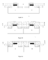
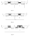
- Fig. 4 represents the different process steps in the manufacturing of the semiconductor device containing at least one strained conductive layer.: (a) upon definition of the metal inserted polysilicon (MIPS) gate and the definition of the spacers; (b) dielectric deposition (6) prior to CMP (chemical mechanical polishing); (c) upon CMP of the dielectric layer (6); (d) upon selective removal of one of the polysilicon gates (8); (e) upon filling and CMP of the first strained conductive layer (4); (f) upon deposition of the third strained conductive layer (7) overlying a thin buffer dielectric layer (6').
- MIPS metal inserted polysilicon
- the metal gate layer (3) has an as deposited (intrinsic) work function which depends on the type metal, the thickness of the metal layer, the deposition method and the temperature budget applied.
- the metal gate layer can comprise Mo, Ru, W, Al, co- sputtered silicides (Ni and Si).
- the gate dielectric (2) can comprise Si02, SiON or any high-k material.
- the choice of high-k might have an influence on the stress behavior of the high-k/metal gate stack.
- a first strained conductive layer (4) is deposited upon the metal gate layer (3) by a replacement gate process, in order to avoid high temperature steps which may modify the strain.
- the first strained conductive layer (4) can comprise metal carbides or metal nitrides like TaxCy, WxCy, TixNy, TaxNy.
- the material, the thickness and method of deposition of the first strained conductive layer are chosen in such way that a pre-determined level of strain is induced in the metal gate layer (3) and additionally the adhesion with the metal gate layer is compatible with further processing.
- the replacement gate process further comprises dielectric (e.g. Si-oxide) deposition and dielectric chemical mechanical polishing (CMP) as shown schematically in Figure 4 (b and c), followed by polysilicon (8) gate wet removal in the second region while the first region is masked/protected ( Figure 4(d) ) and the forming of the first strained conductive layer (4) as shown in Figure 4(e) .
- dielectric e.g. Si-oxide
- CMP dielectric chemical mechanical polishing
- a FUSI gate can be formed on the NMOS region.
- a dielectric buffer layer (6) can be deposited followed by the deposition of a third strained conductive (TiN, W) layer.
- Figure 5 represents schematically PMOS metal gate with a first strained conductive layer (4) and NMOS metal gate with a second strained conductive layer (10).
Landscapes
- Metal-Oxide And Bipolar Metal-Oxide Semiconductor Integrated Circuits (AREA)
- Electrodes Of Semiconductors (AREA)
- Insulated Gate Type Field-Effect Transistor (AREA)
Priority Applications (3)
| Application Number | Priority Date | Filing Date | Title |
|---|---|---|---|
| JP2008288773A JP2009152562A (ja) | 2007-11-13 | 2008-11-11 | ストレッサ層を有するデュアル仕事関数デバイスおよびその製造方法 |
| US12/269,754 US20090174003A1 (en) | 2007-11-13 | 2008-11-12 | Dual work function device with stressor layer and method for manufacturing the same |
| TW097143823A TWI496246B (zh) | 2007-11-13 | 2008-11-13 | 雙功函數半導體元件及其製法 |
Applications Claiming Priority (1)
| Application Number | Priority Date | Filing Date | Title |
|---|---|---|---|
| US98771207P | 2007-11-13 | 2007-11-13 |
Publications (1)
| Publication Number | Publication Date |
|---|---|
| EP2061076A1 true EP2061076A1 (fr) | 2009-05-20 |
Family
ID=39709347
Family Applications (1)
| Application Number | Title | Priority Date | Filing Date |
|---|---|---|---|
| EP08157942A Ceased EP2061076A1 (fr) | 2007-11-13 | 2008-06-10 | Dispositif à travail de sortie dual avec couche de mise sous contrainte et son procédé de fabrication |
Country Status (5)
| Country | Link |
|---|---|
| US (1) | US20090174003A1 (fr) |
| EP (1) | EP2061076A1 (fr) |
| JP (1) | JP2009152562A (fr) |
| CN (1) | CN101471303A (fr) |
| TW (1) | TWI496246B (fr) |
Families Citing this family (14)
| Publication number | Priority date | Publication date | Assignee | Title |
|---|---|---|---|---|
| CN102064133B (zh) * | 2009-11-11 | 2013-03-27 | 中国科学院微电子研究所 | 一种制造半导体器件的方法 |
| US8313990B2 (en) | 2009-12-04 | 2012-11-20 | International Business Machines Corporation | Nanowire FET having induced radial strain |
| US8309991B2 (en) * | 2009-12-04 | 2012-11-13 | International Business Machines Corporation | Nanowire FET having induced radial strain |
| JP5569243B2 (ja) | 2010-08-09 | 2014-08-13 | ソニー株式会社 | 半導体装置及びその製造方法 |
| US8704280B2 (en) * | 2011-09-22 | 2014-04-22 | Taiwan Semiconductor Manufacturing Company, Ltd. | Semiconductor device with strained channels induced by high-k capping metal layers |
| CN103077969B (zh) * | 2011-10-26 | 2016-03-30 | 中国科学院微电子研究所 | 一种mos器件及其制造方法 |
| WO2013082474A1 (fr) * | 2011-11-30 | 2013-06-06 | Ulterius Technologies, Llc | Architecture de puce d'ordinateur |
| US9142414B2 (en) * | 2011-12-20 | 2015-09-22 | Taiwan Semiconductor Manufacturing Company, Ltd. | CMOS devices with metal gates and methods for forming the same |
| US9105498B2 (en) * | 2012-03-01 | 2015-08-11 | International Business Machines Corporation | Gate strain induced work function engineering |
| CN103311281B (zh) * | 2012-03-14 | 2016-03-30 | 中国科学院微电子研究所 | 半导体器件及其制造方法 |
| CN103545179B (zh) * | 2012-07-10 | 2016-05-25 | 中芯国际集成电路制造(上海)有限公司 | 半导体器件及其形成方法 |
| US8952431B2 (en) * | 2013-05-09 | 2015-02-10 | International Business Machines Corporation | Stacked carbon-based FETs |
| DE102013210624B4 (de) * | 2013-06-07 | 2016-09-29 | Globalfoundries Inc. | Verfahren zur Herstellung einer Halbleiterstruktur mit einer Implantation von Ionen in ein Kanalgebiet |
| US9564431B2 (en) | 2014-02-19 | 2017-02-07 | Taiwan Semiconductor Manufacturing Company Limited | Semiconductor structures and methods for multi-level work function |
Citations (4)
| Publication number | Priority date | Publication date | Assignee | Title |
|---|---|---|---|---|
| US20060081942A1 (en) * | 2004-10-19 | 2006-04-20 | Tomohiro Saito | Semiconductor device and manufacturing method therefor |
| US20060124974A1 (en) * | 2004-12-15 | 2006-06-15 | International Business Machines Corporation | Structure and method to generate local mechanical gate stress for mosfet channel mobility modification |
| US20060237801A1 (en) * | 2005-04-20 | 2006-10-26 | Jack Kavalieros | Compensating for induced strain in the channels of metal gate transistors |
| US20070138559A1 (en) * | 2005-12-16 | 2007-06-21 | Intel Corporation | Replacement gates to enhance transistor strain |
Family Cites Families (6)
| Publication number | Priority date | Publication date | Assignee | Title |
|---|---|---|---|---|
| JP2001160594A (ja) * | 1999-09-20 | 2001-06-12 | Toshiba Corp | 半導体装置 |
| US7902058B2 (en) * | 2004-09-29 | 2011-03-08 | Intel Corporation | Inducing strain in the channels of metal gate transistors |
| US7488656B2 (en) * | 2005-04-29 | 2009-02-10 | International Business Machines Corporation | Removal of charged defects from metal oxide-gate stacks |
| US7332433B2 (en) * | 2005-09-22 | 2008-02-19 | Sematech Inc. | Methods of modulating the work functions of film layers |
| TWI267926B (en) * | 2005-09-23 | 2006-12-01 | Ind Tech Res Inst | A new method for high mobility enhancement strained channel CMOS with single workfunction metal-gate |
| US7504289B2 (en) * | 2005-10-26 | 2009-03-17 | Freescale Semiconductor, Inc. | Process for forming an electronic device including transistor structures with sidewall spacers |
-
2008
- 2008-06-10 EP EP08157942A patent/EP2061076A1/fr not_active Ceased
- 2008-11-11 JP JP2008288773A patent/JP2009152562A/ja active Pending
- 2008-11-12 US US12/269,754 patent/US20090174003A1/en not_active Abandoned
- 2008-11-13 CN CNA2008101733521A patent/CN101471303A/zh active Pending
- 2008-11-13 TW TW097143823A patent/TWI496246B/zh active
Patent Citations (4)
| Publication number | Priority date | Publication date | Assignee | Title |
|---|---|---|---|---|
| US20060081942A1 (en) * | 2004-10-19 | 2006-04-20 | Tomohiro Saito | Semiconductor device and manufacturing method therefor |
| US20060124974A1 (en) * | 2004-12-15 | 2006-06-15 | International Business Machines Corporation | Structure and method to generate local mechanical gate stress for mosfet channel mobility modification |
| US20060237801A1 (en) * | 2005-04-20 | 2006-10-26 | Jack Kavalieros | Compensating for induced strain in the channels of metal gate transistors |
| US20070138559A1 (en) * | 2005-12-16 | 2007-06-21 | Intel Corporation | Replacement gates to enhance transistor strain |
Non-Patent Citations (2)
| Title |
|---|
| LOSKUTOV S V: "Work function for the deformed metal surface", SURFACE SCIENCE, NORTH-HOLLAND PUBLISHING CO, AMSTERDAM, NL, vol. 585, no. 1-2, 1 July 2005 (2005-07-01), pages L166 - L170, XP004932476, ISSN: 0039-6028 * |
| PARK SEONGJUN ET AL: "Ab initio study of metal gate electrode work function", APPLIED PHYSICS LETTERS, AIP, AMERICAN INSTITUTE OF PHYSICS, MELVILLE, NY, vol. 86, no. 7, 11 February 2005 (2005-02-11), pages 73118 - 073118, XP012066398, ISSN: 0003-6951 * |
Also Published As
| Publication number | Publication date |
|---|---|
| TW200939401A (en) | 2009-09-16 |
| TWI496246B (zh) | 2015-08-11 |
| US20090174003A1 (en) | 2009-07-09 |
| JP2009152562A (ja) | 2009-07-09 |
| CN101471303A (zh) | 2009-07-01 |
Similar Documents
| Publication | Publication Date | Title |
|---|---|---|
| EP2061076A1 (fr) | Dispositif à travail de sortie dual avec couche de mise sous contrainte et son procédé de fabrication | |
| US7812414B2 (en) | Hybrid process for forming metal gates | |
| US6921913B2 (en) | Strained-channel transistor structure with lattice-mismatched zone | |
| US8361851B2 (en) | Method for manufacturing an NMOS with improved carrier mobility | |
| US7138310B2 (en) | Semiconductor devices having strained dual channel layers | |
| US9240351B2 (en) | Field effect transistor device with improved carrier mobility and method of manufacturing the same | |
| CN103022126B (zh) | 具有由高k保护金属层诱导的应变沟道的半导体器件 | |
| CN102237399B (zh) | 具有金属栅极的半导体元件及其制作方法 | |
| US20080286916A1 (en) | Methods of stressing transistor channel with replaced gate | |
| US20130087856A1 (en) | Effective Work Function Modulation by Metal Thickness and Nitrogen Ratio for a Last Approach CMOS Gate | |
| US8110459B2 (en) | MOSFET having a channel region with enhanced stress and method of forming same | |
| WO2008147433A2 (fr) | Procédés et dispositifs utilisant des couches de métal dans des grilles afin d'introduire une contrainte de canal | |
| US10553497B2 (en) | Methods and devices for enhancing mobility of charge carriers | |
| US20070267694A1 (en) | Transistors with stressed channels and methods of manufacture | |
| US20090298244A1 (en) | Mobility Enhanced FET Devices | |
| US7960795B2 (en) | Partially and fully silicided gate stacks | |
| US7351994B2 (en) | Noble high-k device | |
| US20100025778A1 (en) | Transistor structure and method of making the same | |
| JP2010161400A (ja) | 半導体装置とその製造方法 |
Legal Events
| Date | Code | Title | Description |
|---|---|---|---|
| PUAI | Public reference made under article 153(3) epc to a published international application that has entered the european phase |
Free format text: ORIGINAL CODE: 0009012 |
|
| AK | Designated contracting states |
Kind code of ref document: A1 Designated state(s): AT BE BG CH CY CZ DE DK EE ES FI FR GB GR HR HU IE IS IT LI LT LU LV MC MT NL NO PL PT RO SE SI SK TR |
|
| AX | Request for extension of the european patent |
Extension state: AL BA MK RS |
|
| RAP1 | Party data changed (applicant data changed or rights of an application transferred) |
Owner name: TAIWAN SEMICONDUCTOR MANUFACTURING COMPANY, LTD. ( Owner name: IMEC |
|
| 17P | Request for examination filed |
Effective date: 20091102 |
|
| AKX | Designation fees paid |
Designated state(s): AT BE BG CH CY CZ DE DK EE ES FI FR GB GR HR HU IE IS IT LI LT LU LV MC MT NL NO PL PT RO SE SI SK TR |
|
| 17Q | First examination report despatched |
Effective date: 20100810 |
|
| STAA | Information on the status of an ep patent application or granted ep patent |
Free format text: STATUS: THE APPLICATION HAS BEEN REFUSED |
|
| 18R | Application refused |
Effective date: 20120920 |