EP2061101A2 - Piezoelektrische Vorrichtung, Winkelgeschwindigkeitssensor und Verfahren zur Herstellung der piezoelektrischen Vorrichtung - Google Patents
Piezoelektrische Vorrichtung, Winkelgeschwindigkeitssensor und Verfahren zur Herstellung der piezoelektrischen Vorrichtung Download PDFInfo
- Publication number
- EP2061101A2 EP2061101A2 EP08018395A EP08018395A EP2061101A2 EP 2061101 A2 EP2061101 A2 EP 2061101A2 EP 08018395 A EP08018395 A EP 08018395A EP 08018395 A EP08018395 A EP 08018395A EP 2061101 A2 EP2061101 A2 EP 2061101A2
- Authority
- EP
- European Patent Office
- Prior art keywords
- piezoelectric
- film
- less
- piezoelectric device
- electrode film
- Prior art date
- Legal status (The legal status is an assumption and is not a legal conclusion. Google has not performed a legal analysis and makes no representation as to the accuracy of the status listed.)
- Withdrawn
Links
Images







Classifications
-
- H—ELECTRICITY
- H10—SEMICONDUCTOR DEVICES; ELECTRIC SOLID-STATE DEVICES NOT OTHERWISE PROVIDED FOR
- H10N—ELECTRIC SOLID-STATE DEVICES NOT OTHERWISE PROVIDED FOR
- H10N30/00—Piezoelectric or electrostrictive devices
- H10N30/30—Piezoelectric or electrostrictive devices with mechanical input and electrical output, e.g. functioning as generators or sensors
- H10N30/302—Sensors
-
- C—CHEMISTRY; METALLURGY
- C04—CEMENTS; CONCRETE; ARTIFICIAL STONE; CERAMICS; REFRACTORIES
- C04B—LIME, MAGNESIA; SLAG; CEMENTS; COMPOSITIONS THEREOF, e.g. MORTARS, CONCRETE OR LIKE BUILDING MATERIALS; ARTIFICIAL STONE; CERAMICS; REFRACTORIES; TREATMENT OF NATURAL STONE
- C04B35/00—Shaped ceramic products characterised by their composition; Ceramics compositions; Processing powders of inorganic compounds preparatory to the manufacturing of ceramic products
- C04B35/01—Shaped ceramic products characterised by their composition; Ceramics compositions; Processing powders of inorganic compounds preparatory to the manufacturing of ceramic products based on oxide ceramics
- C04B35/46—Shaped ceramic products characterised by their composition; Ceramics compositions; Processing powders of inorganic compounds preparatory to the manufacturing of ceramic products based on oxide ceramics based on titanium oxides or titanates
- C04B35/462—Shaped ceramic products characterised by their composition; Ceramics compositions; Processing powders of inorganic compounds preparatory to the manufacturing of ceramic products based on oxide ceramics based on titanium oxides or titanates based on titanates
- C04B35/472—Shaped ceramic products characterised by their composition; Ceramics compositions; Processing powders of inorganic compounds preparatory to the manufacturing of ceramic products based on oxide ceramics based on titanium oxides or titanates based on titanates based on lead titanates
-
- C—CHEMISTRY; METALLURGY
- C04—CEMENTS; CONCRETE; ARTIFICIAL STONE; CERAMICS; REFRACTORIES
- C04B—LIME, MAGNESIA; SLAG; CEMENTS; COMPOSITIONS THEREOF, e.g. MORTARS, CONCRETE OR LIKE BUILDING MATERIALS; ARTIFICIAL STONE; CERAMICS; REFRACTORIES; TREATMENT OF NATURAL STONE
- C04B35/00—Shaped ceramic products characterised by their composition; Ceramics compositions; Processing powders of inorganic compounds preparatory to the manufacturing of ceramic products
- C04B35/01—Shaped ceramic products characterised by their composition; Ceramics compositions; Processing powders of inorganic compounds preparatory to the manufacturing of ceramic products based on oxide ceramics
- C04B35/48—Shaped ceramic products characterised by their composition; Ceramics compositions; Processing powders of inorganic compounds preparatory to the manufacturing of ceramic products based on oxide ceramics based on zirconium or hafnium oxides, zirconates, zircon or hafnates
- C04B35/49—Shaped ceramic products characterised by their composition; Ceramics compositions; Processing powders of inorganic compounds preparatory to the manufacturing of ceramic products based on oxide ceramics based on zirconium or hafnium oxides, zirconates, zircon or hafnates containing also titanium oxides or titanates
- C04B35/491—Shaped ceramic products characterised by their composition; Ceramics compositions; Processing powders of inorganic compounds preparatory to the manufacturing of ceramic products based on oxide ceramics based on zirconium or hafnium oxides, zirconates, zircon or hafnates containing also titanium oxides or titanates based on lead zirconates and lead titanates, e.g. PZT
-
- G—PHYSICS
- G01—MEASURING; TESTING
- G01C—MEASURING DISTANCES, LEVELS OR BEARINGS; SURVEYING; NAVIGATION; GYROSCOPIC INSTRUMENTS; PHOTOGRAMMETRY OR VIDEOGRAMMETRY
- G01C19/00—Gyroscopes; Turn-sensitive devices using vibrating masses; Turn-sensitive devices without moving masses; Measuring angular rate using gyroscopic effects
- G01C19/56—Turn-sensitive devices using vibrating masses, e.g. vibratory angular rate sensors based on Coriolis forces
- G01C19/5642—Turn-sensitive devices using vibrating masses, e.g. vibratory angular rate sensors based on Coriolis forces using vibrating bars or beams
- G01C19/5663—Manufacturing; Trimming; Mounting; Housings
-
- H—ELECTRICITY
- H10—SEMICONDUCTOR DEVICES; ELECTRIC SOLID-STATE DEVICES NOT OTHERWISE PROVIDED FOR
- H10N—ELECTRIC SOLID-STATE DEVICES NOT OTHERWISE PROVIDED FOR
- H10N30/00—Piezoelectric or electrostrictive devices
- H10N30/80—Constructional details
- H10N30/85—Piezoelectric or electrostrictive active materials
- H10N30/853—Ceramic compositions
- H10N30/8548—Lead-based oxides
- H10N30/8554—Lead-zirconium titanate [PZT] based
-
- C—CHEMISTRY; METALLURGY
- C04—CEMENTS; CONCRETE; ARTIFICIAL STONE; CERAMICS; REFRACTORIES
- C04B—LIME, MAGNESIA; SLAG; CEMENTS; COMPOSITIONS THEREOF, e.g. MORTARS, CONCRETE OR LIKE BUILDING MATERIALS; ARTIFICIAL STONE; CERAMICS; REFRACTORIES; TREATMENT OF NATURAL STONE
- C04B2235/00—Aspects relating to ceramic starting mixtures or sintered ceramic products
- C04B2235/70—Aspects relating to sintered or melt-casted ceramic products
- C04B2235/74—Physical characteristics
- C04B2235/76—Crystal structural characteristics, e.g. symmetry
-
- C—CHEMISTRY; METALLURGY
- C04—CEMENTS; CONCRETE; ARTIFICIAL STONE; CERAMICS; REFRACTORIES
- C04B—LIME, MAGNESIA; SLAG; CEMENTS; COMPOSITIONS THEREOF, e.g. MORTARS, CONCRETE OR LIKE BUILDING MATERIALS; ARTIFICIAL STONE; CERAMICS; REFRACTORIES; TREATMENT OF NATURAL STONE
- C04B2235/00—Aspects relating to ceramic starting mixtures or sintered ceramic products
- C04B2235/70—Aspects relating to sintered or melt-casted ceramic products
- C04B2235/74—Physical characteristics
- C04B2235/76—Crystal structural characteristics, e.g. symmetry
- C04B2235/765—Tetragonal symmetry
-
- C—CHEMISTRY; METALLURGY
- C04—CEMENTS; CONCRETE; ARTIFICIAL STONE; CERAMICS; REFRACTORIES
- C04B—LIME, MAGNESIA; SLAG; CEMENTS; COMPOSITIONS THEREOF, e.g. MORTARS, CONCRETE OR LIKE BUILDING MATERIALS; ARTIFICIAL STONE; CERAMICS; REFRACTORIES; TREATMENT OF NATURAL STONE
- C04B2235/00—Aspects relating to ceramic starting mixtures or sintered ceramic products
- C04B2235/70—Aspects relating to sintered or melt-casted ceramic products
- C04B2235/74—Physical characteristics
- C04B2235/79—Non-stoichiometric products, e.g. perovskites (ABO3) with an A/B-ratio other than 1
-
- H—ELECTRICITY
- H10—SEMICONDUCTOR DEVICES; ELECTRIC SOLID-STATE DEVICES NOT OTHERWISE PROVIDED FOR
- H10N—ELECTRIC SOLID-STATE DEVICES NOT OTHERWISE PROVIDED FOR
- H10N30/00—Piezoelectric or electrostrictive devices
- H10N30/80—Constructional details
- H10N30/87—Electrodes or interconnections, e.g. leads or terminals
Definitions
- the present invention contains subject matter related to Japanese Patent Application JP 2007-297321 filed in the Japanese Patent Office on November 15, 2007, Japanese Patent Application JP 2007-297323 filed in the Japanese Patent Office on November 15, 2007, and Japanese Patent Application JP 2007-297325 filed in the Japanese Patent Office on November 15, 2007, the entire contents of which being incorporated herein by reference.
- the present invention relates to a piezoelectric device used in a piezoelectric sensor, a piezoelectric actuator, and a pyroelectric infrared ray sensor, an angular velocity sensor including the piezoelectric device, and a method of manufacturing a piezoelectric device.
- PZT lead zirconium titanate
- a piezoelectric material of a piezoelectric thin film used for a piezoelectric sensor such as an angular velocity sensor, an ink jet head, and the like.
- Various techniques are proposed for improving piezoelectric characteristics, ferromagnetic material characteristics, pyroelectric characteristics, and the like of the PZT (see, for example, Japanese Patent Application Laid-open No. Hei 06-350154 (paragraphs (0030) to (0044), (0060) to (0073), Figs.
- Patent Document 1 Japanese Patent Application Laid-open No. Hei 09-298324 (paragraphs (0007) to (0009), Fig. 5 ); hereinafter, will respectively be referred to as Patent Document 1 and Patent Document 2).
- Patent Document 1 discloses a PZT thin film whose crystalline structure is rhombohedral, in which, when lead zirconium titanate is represented by Pb 1+Y (Zr X Ti 1-X )O 3+Y , a PbO excessive composition ratio Y is within a range of 0 ⁇ Y ⁇ 0.5, and a Zr composition ratio X is within a range of 0 ⁇ X ⁇ 0.55.
- the PZT thin film of Patent Document 1 exhibits favorable piezoelectric characteristics.
- a PZT thin film whose crystalline structure is tetragonal, in which the PbO excessive composition ratio Y is within a range of 0 ⁇ Y ⁇ 0.5, and the Zr composition ratio X is within a range of 0.55 ⁇ X ⁇ 1.
- Patent Document 2 discloses a piezoelectric thin film having a thickness of 1 ⁇ m or more and 10 ⁇ m or less, a crystal grain size of 0.55 ⁇ m or less, and surface roughness of 1 ⁇ m or less at R MAX .
- the piezoelectric thin film is useful as a piezoelectric thin film for an inkjet-type storage apparatus that requires a predetermined film thickness or more.
- the piezoelectric material when heated, the piezoelectric material is known to deteriorate in piezoelectric performance, which is called depolarization.
- heating processing by solder reflow and the like is generally carried out in a process of manufacturing an electronic apparatus that includes the piezoelectric material, there is a problem that the piezoelectric performance of the piezoelectric material deteriorates due to the heat.
- Patent Documents 1 and 2 above give no consideration to the effect of heat.
- a piezoelectric device including a piezoelectric film and an electrode film.
- the piezoelectric film is constituted of lead zirconium titanate represented by Pb 1+X (Zr Y Ti 1-Y )O 3+X , where X is 0 or more and 0.3 or less and Y is 0 or more and 0.55 or less, the piezoelectric film having a tension stress.
- the electrode film applies a voltage to the piezoelectric film.
- a piezoelectric device excellent in piezoelectric characteristics can be obtained. If the Zr composition ratio Y is 0 or more and 0.55 or less, depolarization hardly occurs and excellent heat resistance can be obtained.
- the tension stress of the piezoelectric film may be 50 MPa or more and 500 MPa or less. Accordingly, a piezoelectric device with additionally-improved heat resistance can be obtained.
- the piezoelectric film may have a film thickness of 400 nm or more and 1,000 nm or less.
- the electrode film may have a tension stress of 500 MPa or more and 1,500 MPa or less.
- the piezoelectric film may have an orientation of 80% or more in a ⁇ 111> direction.
- the piezoelectric film may include at least one of additive elements selected from the group consisting of Cr, Mn, Fe, Ni, Mg, Sn, Cu, Ag, Nb, Sb, and N.
- the electrode film may be formed of at least one of Ti and Pt.
- the electrode film may also be formed of Ir, Au, and Ru, or oxides of Ti, Pt, Ir, Au, and Ru.
- a piezoelectric device including a piezoelectric film and an electrode film.
- the piezoelectric film is constituted of lead zirconium titanate represented by Pb 1+X (Zr Y Ti 1-Y )O 3+X , where X is 0 or more and 0.3 or less and Y is 0 or more and 0.55 or less.
- the electrode film has a tension stress of 500 MPa or more and 1,500 MPa or less and applies a voltage to the piezoelectric film.
- the PbO excessive composition ratio X of the PZT is 0 or more and 0.3 or less and the Zr composition ratio Y to be 0 or more and 0.55 or less, a piezoelectric device excellent in piezoelectric characteristics can be obtained. If the Zr composition ratio Y is 0 or more and 0.55 or less, depolarization hardly occurs and excellent heat resistance can be obtained.
- the piezoelectric film may have a film thickness of 400 nm or more and 1,000 nm or less.
- the piezoelectric film may have a tension stress of 50 MPa or more and 500 MPa or less.
- the piezoelectric film may have an orientation of 80% or more in a ⁇ 111> direction.
- the piezoelectric film may include at least one of additive elements selected from the group consisting of Cr, Mn, Fe, Ni, Mg, Sn, Cu, Ag, Nb, Sb, and N.
- the electrode film may be formed of at least one of Ti and Pt.
- the electrode film may also be formed of Ir, Au, and Ru, or oxides of Ti, Pt, Ir, Au, and Ru.
- a piezoelectric device including a piezoelectric film and an electrode film.
- the piezoelectric film is constituted of lead zirconium titanate represented by Pb 1+X (Zr Y Ti 1-Y )O 3+X , where X is 0 or more and 0.3 or less and Y is 0 or more and 0.55 or less, the piezoelectric film having a film thickness of 400 nm or more and 1,000 nm or less.
- the electrode film applies a voltage to the piezoelectric film.
- the PbO excessive composition ratio X of the PZT is 0 or more and 0.3 or less and the Zr composition ratio Y to be 0 or more and 0.55 or less, a piezoelectric device excellent in piezoelectric characteristics can be obtained. If the Zr composition ratio Y is 0 or more and 0.55 or less, depolarization hardly occurs and excellent heat resistance can be obtained.
- the film thickness is 400 nm or more and 1,000 nm or less, a piezoelectric device with additionally-improved piezoelectric characteristics can be obtained.
- the piezoelectric film may have an orientation of 80% or more in a ⁇ 111> direction.
- the piezoelectric film may include at least one of additive elements selected from the group consisting of Cr, Mn, Fe, Ni, Mg, Sn, Cu, Ag, Nb, Sb, and N.
- the electrode film may be formed of at least one of Ti and Pt.
- the electrode film may also be formed of Ir, Au, and Ru, or oxides of Ti, Pt, Ir, Au, and Ru.
- an angular velocity sensor including a substrate, a first electrode film, a piezoelectric film, and a second electrode film.
- the first electrode film is formed on the substrate.
- the piezoelectric film is constituted of lead zirconium titanate represented by Pb 1+X (Zr Y Ti 1-Y )O 3+X , where X is 0 or more and 0.3 or less and Y is 0 or more and 0.55 or less, the piezoelectric film having a tension stress and formed on the first electrode film.
- the second electrode film is formed on the piezoelectric film.
- an angular velocity sensor including a substrate, a first electrode film, a piezoelectric film, and a second electrode film.
- the first electrode film has a tension stress of 500 MPa or more and 1,500 MPa or less and is formed on the substrate.
- the piezoelectric film is constituted of lead zirconium titanate represented by Pb 1+X (Zr Y Ti 1-Y )O 3+X , where X is 0 or more and 0.3 or less and Y is 0 or more and 0.55 or less, the piezoelectric film formed on the first electrode film.
- the second electrode film is formed on the piezoelectric film.
- an angular velocity sensor including a substrate, a first electrode film, a piezoelectric film, and a second electrode film.
- the first electrode film is formed on the substrate.
- the piezoelectric film is constituted of lead zirconium titanate represented by Pb 1+X (Zr Y Ti 1-Y )O 3+X , where X is 0 or more and 0.3 or less and Y is 0 or more and 0.55 or less, the piezoelectric film having a film thickness of 400 nm or more and 1,000 nm or less and formed on the first electrode film.
- the second electrode film is formed on the piezoelectric film.
- a piezoelectric device excellent in piezoelectric characteristics and heat resistance an angular velocity sensor including the piezoelectric device, and a method of manufacturing a piezoelectric device can be provided.
- FIGs. 1 are diagrams showing a piezoelectric device and an angular velocity sensor including the piezoelectric device according to the first embodiment of the present invention.
- An angular velocity sensor 31 includes a base body 130 and a vibration arm 132 that extends from the base body 130 and is capable of vibrating.
- Fig. 1B is a cross-sectional diagram of a surface vertical to a longitudinal axis (Z axis) of the vibration arm 132.
- the angular velocity sensor 31 includes a semiconductor arm base 133 made of, for example, silicon, and a piezoelectric device 139 disposed on the arm base 133.
- a first electrode film 34a as a common electrode is laminated on a silicon substrate, and a piezoelectric film 33 is laminated on the first electrode film 34a.
- a second electrode film 34b, a first detection electrode 34c, and a second detection electrode 34d are formed on a first surface 33a as an upper surface of the piezoelectric film 33.
- a lead electrode including lead wires 136, electrode pads 138, bumps 134a to 134d, and the like is formed on the base body 130.
- the bump 134a is connected to the second electrode film 34b
- the bumps 134b and 134c are respectively connected to the first detection electrode 34c and the second detection electrode 34d
- the bump 134d is connected to the first electrode film 34a.
- An external connection to a control circuit (not shown) such as an IC is made via the bumps 134a to 134d.
- the bumps 134a to 134d are each formed of metal, for example, but are not limited thereto.
- the angular velocity sensor 31 of a shape as shown in Fig. 1A is cut out from a silicon wafer.
- the first electrode film 34a of the piezoelectric device 139 is connected to a DC power supply, and an AC power supply is connected between a first electrode film 34a and the second electrode film 34b. Accordingly, a voltage is applied to the piezoelectric film 33 disposed between the first electrode film 34a and the second electrode film 34b so that the vibration arm 132 is caused of a flexion movement in a vertical direction (Y direction).
- Coriolis force is generated in the vibration arm 132.
- the Coriolis force is generated in a direction vertical (X direction) to a direction of the flexion movement of the vibration arm 132 (Y direction), a magnitude of which is proportional to a value of the applied angular velocity ⁇ 0 .
- the Coriolis force is converted into an electric signal by the piezoelectric film 33, and the converted signal is detected by the first detection electrode 34c and the second detection electrode 34d.
- piezoelectric performance and heat resistance performance of the piezoelectric device 139 will be described while describing a method of manufacturing the angular velocity sensor 31. It should be noted that descriptions will mainly be given on a method of forming the piezoelectric device 139 formed on the arm base 133.
- a silicon wafer is prepared.
- An oxidation protection film may be formed on the silicon wafer by thermal oxidation processing.
- the first electrode film 34a is formed by depositing Ti of 30 nm on the silicon wafer by a sputtering method, and then depositing Pt of 100 nm thereon, for example.
- the deposition method of the first electrode film 34a is not limited to the sputtering method, and a vacuum vapor deposition method or other deposition methods may be used.
- the metal materials that constitute the first electrode film 34a are not limited to Ti and Pt, and examples thereof include Ir, Au, and Ru, or oxides of Ti, Pt, Ir, Au, and Ru.
- the second electrode film 34b may also be constituted of those metal materials.
- the piezoelectric film 33 is formed by forming a PZT thin film on the first electrode film 34a by, for example, the sputtering method.
- the deposition method of the piezoelectric film 33 is not limited to the sputtering method, and deposition methods such as a vacuum vapor deposition method, a PLD (pulsed laser deposition) method, a sol-gel method, an aerosol deposition method, and the like may be used.
- a substrate temperature when depositing the PZT thin film 33 may either be at room temperature or at a high temperature.
- a PbO excessive composition ratio X is set to be -0.1 or more and 0.5 or less
- a Zr composition ratio Y is set to be 0.35 or more and 0.65 or less.
- a target composition, sputtering conditions, annealing conditions, and the like are set appropriately.
- heating processing at 700° for example, may be carried out on the PZT thin film 33.
- a crystalline structure of the PZT thin film 33 in this case is tetragonal.
- a film thickness of the PZT thin film 33 formed as described above is 100 nm to 1,400 nm.
- the second electrode film 34b is deposited on the PZT thin film 33 by the sputtering method to thus form the second electrode film 34b.
- the deposition method of the second electrode film 34b in this case is not limited to the sputtering method, and a vacuum vapor deposition method or other deposition methods may be used.
- a voltage is applied between the first electrode film 34a and the second electrode film 34b in an atmosphere heated to 240°, and polarization processing is carried out on the PZT thin film 33.
- the voltage applied between the first electrode film 34a and the second electrode film 34b is 1 to 20-times as large as a coercive electric field E c .
- a polarization temperature in the polarization processing is, compared to a Curie temperature, 1/16 to 5/4 the Curie temperature. It should be noted that the polarization processing may be carried out in any of an atmosphere, an oxygen atmosphere, and a nitrogen atmosphere.
- prebake processing is carried out on the deposited PZT thin film 33.
- a prebake temperature of the prebake processing is 1/2 to 5/4 the Curie temperature.
- the PZT thin film 33 described above may have a tension stress.
- the PZT thin film 33 may be subjected to heating processing at, for example, 650°C to 750°C after being formed on the first electrode film 34a. Accordingly, crystallization of the PZT thin film 33 is accelerated, thus obtaining the tension stress.
- the target composition, the sputtering conditions, the annealing conditions, and the like are set appropriately such that the PbO excessive composition ratio X of the PZT becomes 0.04, the Zr composition ratio Y thereof becomes 0.35 to 0.65, and the tension stress becomes -100 MPa to 600 MPa, for example.
- the first electrode film 34a described above may also have the tension stress.
- the first electrode film 34a may be subjected to the heating processing at, for example, 100°C to 800°C after the PZT thin film 33 is formed thereon.
- the tension stress of the first electrode film 34a formed as described above is -200 MPa to 2,000 MPa.
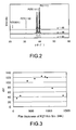
- Fig. 2 is a diagram showing an XRD (X-ray diffraction) pattern of the PZT thin film 33.
- the PZT is oriented to a ⁇ 111> surface and has an orientation degree of 97%.
- the film thickness of the PZT thin film 33 whose XRD pattern has been measured is 900 nm
- the voltage used in the polarization processing is 6-times the coercive electric field
- the polarization temperature is 240°C.
- the prebake temperature is 200°C for 100s.
- the film thickness of the PZT thin film 33 is 900 nm.
- Fig. 3 is a diagram showing a relationship between the film thickness (100 nm to 1,400 nm) of the PZT thin film 33 and a piezoelectric constant d31.
- the PZT thin film 33 shows favorable piezoelectric characteristics when the film thickness is 400 nm to 1,000 nm. Consequently, piezoelectric characteristics sufficient for the piezoelectric device 139 of the angular velocity sensor 31 can be obtained when the film thickness is within the range of 400 nm to 1,000 nm.
- the piezoelectric constant d31 decreases when the film thickness of the PZT thin film 33 is 1,000 nm or more. This is probably because when the film thickness is 1,000 nm or more, crystals grow in a direction other than the ⁇ 111> surface direction, such as a ⁇ 001> surface direction, and thus a peak intensity in the ⁇ 111> surface direction is saturated. Therefore, by setting the film thickness of the PZT thin film 33 to be less than 1,000 nm, peak growths in directions other than the ⁇ 111> surface direction can be suppressed. It should be noted that a main peak of a crystal mainly contributes to the piezoelectric characteristics.
- the film thickness of less than 400 nm leads to an increase in leak current, whereby it becomes difficult to obtain piezoelectric characteristics sufficient for the piezoelectric device 139.
- Fig. 4 is a diagram showing relationships of the PbO excessive composition ratio X (-0.1 to 0.5) of the PZT thin film 33 with the piezoelectric constant d31 and a loss rate tan ⁇ .
- the orientation degree of the PZT thin film 33 in the ⁇ 111> surface direction is 80% or more and less than 100%, and the Zr composition ratio Y is 0.5.
- the piezoelectric constant d31 and the loss rate tan ⁇ are both favorable when the PbO excessive composition ratio X is within the range of 0 to 0.3.
- the piezoelectric characteristics deteriorate when the PbO excessive composition ratio X is less than 0. This is probably because PZT crystallinity deteriorates when the PbO excessive composition ratio X is small.
- the loss rate tan ⁇ increases and the piezoelectric characteristics deteriorate when the PbO excessive composition ratio X is 0.3 or more. This is probably because an insulation property of the PZT thin film 33 deteriorates when the PbO excessive composition ratio X is large, thus resulting in a decrease in piezoelectric characteristics.
- Fig. 5 is a diagram showing a relationship between the Zr composition ratio Y (0.35 to 0.65) of the PZT thin film 33 and the piezoelectric constant d31.
- the PZT thin film 33 shows maximum piezoelectric characteristics when the Zr composition ratio Y is 0.51 and favorable piezoelectric characteristics when the Zr composition ratio Y is 0.4 or more and 0.55 or less.
- the Zr composition ratio Y is 0.4 or more and 0.55 or less, piezoelectric characteristics sufficient for the piezoelectric device 139 of the angular velocity sensor 31 can be obtained.
- a bulk PZT shows favorable piezoelectric characteristics when the Zr composition ratio Y thereof is 0.5 or more and 0.53 or less.
- the piezoelectric characteristics of the bulk PZT deteriorate precipitously when the Zr composition ratio Y becomes less than 0.5.
- the PZT thin film deposited by, for example, the sputtering method shows favorable piezoelectric characteristics even when the Zr composition ratio Y is 0.4 or more and 0.5 or less.
- the angular velocity sensor 31 of a shape as shown in Fig. 1A is cut out from the silicon wafer on which the piezoelectric device 139 including the first electrode film 34a, the PZT thin film 33, and second electrode film 34b, the lead wires 136, and the like are formed.
- An MEMS (Micro Electro Mechanical Systems) technique is typically used for the cutout from the silicon wafer. It should be noted that length, width, and thickness of the vibration arm 132 are, for example, 2,000 ⁇ m, 150 ⁇ m, and 150 ⁇ m, respectively.
- the heat resistance is evaluated by measuring an amplitude of the vibration arm 132 of the thus-formed angular velocity sensor 31 in the Y direction.
- the heat resistance of the piezoelectric device 139 is evaluated by measuring the amplitude of the vibration arm 132 in the Y direction, applying to the PZT thin film 33 heat that takes into account the heating processing carried out at the time of manufacturing the device, such as solder reflow, and re-measuring the amplitude of the vibration arm 132 in the Y direction thereafter.
- the heat applied to the PZT thin film 33 is, considering the heating processing at the time of manufacturing the device, 180°C to 300°C, and a heating time thereof is 30s to 300s.
- the voltage applied between the first electrode film 34a and second electrode film 34b is an AC voltage of, for example, 1kHz, 1V.
- Fig. 6 is a diagram showing a relationship between the Zr composition ratio Y (0.35 to 0.7) of the PZT thin film 33 and an attenuation rate of the vibration arm 132 after application of heat.
- the heating temperature and the heating time are 240°C and 90s, respectively.
- Fig. 7 is a diagram showing a relationship between the heating time and the amplitude attenuation rate after application of heat in a case where the heating temperature is set to 240°.
- the Zr composition ratio Y of the PZT thin film 33 is within the range of 0.35 to 0.60. It can be seen from Fig. 7 that when the Zr composition ratio Y is 0.55 or less, the amplitude attenuation after application of heat hardly occurs even when the heating time is extended, which implies excellent heat resistance.
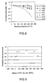
- Fig. 8 is a diagram showing a relationship between the heating temperature and the amplitude attenuation rate after application of heat.
- the Zr composition ratio Y of the PZT thin film 33 is within the range of 0.35 to 0.60. It can be seen from Fig. 8 that when the Zr composition ratio Y is 0.55 or less, the amplitude attenuation after application of heat hardly occurs even when the heating temperature is increased, which implies excellent heat resistance.
- Fig. 9 is a diagram showing a relationship between a stress (-100 MPa to 600 MPa) of the PZT thin film 33 and the amplitude attenuation rate after application of heat.
- the tension stress of the first electrode film 34a is 1,000 MPa.
- the heating temperature and heating time of the PZT thin film 33 are 240°C and 90s, respectively. It should be noted that in Fig. 9 , a stress of a positive value represents a tension stress, and a stress of a negative value represents a compression stress.
- An X-ray reciprocal lattice map measurement method is used as the method of measuring a stress of the PZT thin film 33, and an X-ray diffraction apparatus X'pert PRO MRD (registered trademark) from PANalytical (registered trademark) is used as a measurement apparatus therefor.
- X'pert PRO MRD registered trademark
- PANalytical registered trademark
- a measurement target sample is tilted about a ⁇ axis orthogonal to a ⁇ axis, and diffraction from a crystal surface of the sample is detected. Identification of the measurement target sample is made based on the detected diffraction peak.
- the method of measuring a stress of the PZT thin film 33 is not limited to the X-ray reciprocal lattice map measurement method, and other methods may be used instead.
- a value of the stress may be evaluated by using Stoney Expression after measuring a warpage of a substrate on which a film is deposited (reference: "Basics and Application of Thin Films by a Plasma Process", Hiroshi Ichimura, Masaru Ikenaga, THE NIKKAN KOGYO SHIMBUN, LTD., 2005).
- a nanoindentation method is used as described in the reference, for example.
- the X-ray reciprocal lattice map measurement method, the measurement method described in the reference, or the like is also used as a measurement method of the first electrode film 34a to be described later.
- the amplitude after application of heat is not attenuated when the tension stress of the PZT thin film 33 is 50 MPa or more and 500 MPa or less.
- the PZT thin film 33 with the tension stress of 50 MPa to 500 MPa has favorable heat resistance.
- the PZT thin film 33 with the tension stress of 100 MPa to 300 MPa has favorable heat resistance.
- the reason why the PZT thin film 33 has favorable heat resistance when provided with the tension stress that is within the range described above is that a crystal lattice of the PZT is distorted to thus suppress a movement of domains.
- the amplitude after application of heat is attenuated when the tension stress of the PZT thin film 33 exceeds 500 MPa. This is probably because cracks increase due to the stress of the PZT thin film 33, and the distortion of the crystal lattice is thus eliminated.
- the amplitude after application of heat is attenuated when the tension stress is less than 50 MPa. This is probably because the movement of domains is facilitated since there is no distortion in crystal lattice due to a low stress of the PZT thin film 33.
- Fig. 10 is a diagram showing a relationship between a stress (-500 MPa to 2,000 MPa) of the first electrode film 34a and the amplitude attenuation rate after application of heat.
- the tension stress of the PZT thin film 33 is 200 MPa.
- the heating temperature and heating time of the PZT thin film 33 are 240°C and 90s, respectively.
- the amplitude after application of heat is not attenuated when the tension stress of the first electrode film 34a is 500 MPa or more and 1,500 MPa or less.
- the piezoelectric device 139 including the first electrode film 34a with the tension stress of 500 MPa to 1,500 MPa has favorable heat resistance.
- the PZT thin film 33 formed on the first electrode film 34a has favorable heat resistance.
- the reason why the piezoelectric device 139 has favorable heat resistance when the first electrode film 34a is provided with the tension stress that is within the range described above is that a crystal lattice of the PZT thin film 33 is distorted to an appropriate degree by the tension stress of the first electrode film 34a, to thus suppress the movement of domains.
- the amplitude after application of heat is attenuated when the tension stress of the first electrode film 34a exceeds 1,500 MPa. This is probably because cracks of the PZT thin film 33 increase by the tension stress of first electrode film 34a, and the distortion of the crystal lattice is thus eliminated. In this case, cracks have actually been observed on the surface of the PZT thin film 33. Moreover, a peeling has been observed between the first electrode film 34a having the tension stress of more than 1,500 MPa and the arm base 133.
- the amplitude after application of heat is attenuated also when the tension stress of the first electrode film 34a is less than 500 MPa. This is probably because the movement of domains is facilitated since there is no distortion in crystal lattice due to a low stress of the first electrode film 34a.
- Fig. 11 is a diagram showing a relationship between an orientation degree of the PZT in the ⁇ 111> surface direction and the amplitude attenuation rate of the vibration arm 132 after application of heat.
- the PbO excessive composition ratio X and Zr composition ratio Y of the PZT thin film 33 are 0.04 and 0.48, respectively. It can be seen from Fig. 11 that when the orientation degree of the PZT in the ⁇ 111> surface direction is 80% or more, the amplitude attenuation after application of heat hardly occurs, which implies excellent heat resistance. On the other hand, it can be seen that when the orientation degree of the PZT in the ⁇ 111> surface direction is less than 80%, the amplitude attenuation after application of heat is apt to occur.
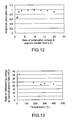
- Fig. 12 is a diagram showing a relationship between a ratio of a polarization voltage in the polarization processing with respect to a coercive electric field (1 to 20-times the coercive electric field E c ) and the amplitude attenuation rate of the vibration arm 132 after application of heat.
- the amplitude attenuation after application of heat hardly occurs when the polarization voltage is 2 to 20-times the coercive electric field E c , which implies excellent heat resistance.
- Fig. 13 shows a relationship between a ratio of a withstanding voltage of the PZT thin film 33 with respect to the coercive electric field and the polarization temperature. As shown in Fig.
- an increase in polarization temperature leads to a decrease in ratio of the withstanding voltage of the PZT with respect to the coercive electric field.
- a dielectric breakdown of the PZT occurs when a polarization voltage that is 20-times or more the coercive electric field is applied to the PZT at the polarization temperature of 180°C or more. Therefore, it can be seen that applying the polarization voltage that is 20-times or more the coercive electric field E c to the PZT is inappropriate, and an appropriate polarization voltage is a voltage that is 2 to 20-times the coercive electric field E c .
- Fig. 14 is a diagram showing a relationship between a ratio of the polarization temperature in the polarization processing with respect to a Curie temperature (1/16 to 5/4 the Curie temperature T c ) and the amplitude attenuation rate after application of heat.
- the polarization voltage is 6-times the coercive electric field E c .
- the amplitude attenuation after application of heat hardly occurs, which implies excellent heat resistance.
- Fig. 15 is a diagram showing relationships of a ratio of a prebake temperature Ta with respect to the Curie temperature (1/2 to 5/4 the Curie temperature T c ), with the amplitude attenuation rate after application of heat (abscissa axis and right-hand side ordinate axis) and a post-baking/post-polarization amplitude attenuation rate (abscissa axis and left-hand side ordinate axis).
- the amplitude attenuation rate in the prebake processing is evaluated by measuring the amplitude of the vibration arm 132 after the polarization processing, and re-measuring the amplitude of the vibration arm 132 after the prebake processing (1/2 to 5/4 the Curie temperature T c ) (abscissa axis and left-hand side ordinate axis).
- the amplitude of the vibration arm 132 after application of heat is measured, and the amplitude attenuation rate after application of heat is thus measured (abscissa axis and right-hand side ordinate axis).
- the polarization voltage is 6-times the coercive electric field E c
- the polarization temperature is 260°C.
- Fig. 16 is a plan diagram showing an angular velocity sensor according to this embodiment.
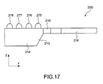
- Fig. 17 is a schematic diagram of the angular velocity sensor according to this embodiment
- Fig. 18 is a cross-sectional diagram taken along the line A-A of Fig. 16 .
- an angular velocity sensor 200 includes a base body 214, an arm retention portion 215 provided on one side of the base body 214, and a vibration arm portion 216 provided on a tip end side of the arm retention portion 215.
- the vibration arm portion 216 includes a first vibration arm 211, and second and third vibration arms 212 and 213 sandwiching the first vibration arm 211.
- the first vibration arm 211 is constituted of an arm base 210a and a piezoelectric device 239a formed thereon
- the second vibration arm 212 is constituted of an arm base 210b and a piezoelectric device 239b formed thereon
- the third vibration arm 213 is constituted of an arm base 210c and a piezoelectric device 239c formed thereon.
- the angular velocity sensor 200 according to this embodiment is a so-called triple-branch tuning-fork type angular velocity sensor.
- the first to third vibration arms 211 to 213 have the same width and thickness, for example. Moreover, a gap between the first and second vibration arms 211 and 212 and a gap between the first and third vibration arms 211 and 213 are the same.
- first electrode films 221 to 223 are respectively formed on the arm bases 210a to 210c, and PZT thin films 231 to 233 each as a piezoelectric film are respectively formed on the first electrode films 221 to 223. Further, second electrode films 241 to 243 each as a drive electrode are respectively formed on the PZT thin films 231 to 233. Moreover, a first detection electrode 251 and a second detection electrode 252 are formed on the piezoelectric thin film 231 of the first vibration arm 211 in the middle of the vibration arm portion 216.
- a film thickness of each of the PZT thin films 231 to 233 and the PbO excessive composition ratio X and Zr composition ratio Y of the PZT are the same as that of the PZT thin film 33 according to the first embodiment. Further, the PZT thin films 231 to 233 each have a tension stress of the same level as the PZT thin film 33. Furthermore, the first electrode films 221 to 223 also have a tension stress of the same level as the first electrode film 34a of the first embodiment.
- the plurality of electrodes 221 to 223, 241 to 243, 251, and 252 included in the respective piezoelectric devices 239 are respectively connected to lead wires 261 to 268.
- the lead wires 261 to 268 pass through a surface of the arm retention portion 215 to be respectively connected to lead terminals 271 to 278 provided on a surface of the base body 214.
- the lead terminals 271 to 278 are provided four each on both sides in an X direction on the surface of the base body 214.
- the first vibration arm 211 is caused of a flexion movement in the vertical direction of Fig. 18 when a voltage is applied to the first electrode film 221 and the second electrode film 241.
- the second and third vibration arms 212 and 213 are caused of a flexion movement in the vertical direction at a phase opposite to that of the first vibration arm 211, when a voltage is applied to the first electrode films 222 and 223 and second electrode films 242 and 243.
- the second and third vibration arms 212 and 213 move downward when the first vibration arm 211 move upward, and the second and third vibration arms 212 and 213 move upward when the first vibration arm 211 move downward. Moreover, by the second and third vibration arms 212 and 213 being caused of the flexion movement at an amplitude half the amplitude of the first vibration arm 211, moments generated by the first to third vibration arms 211 to 213 are canceled out.
- each of the piezoelectric devices 239 has the same piezoelectric performance and heat resistance as the piezoelectric device 139 of the angular velocity sensor 31 according to the first embodiment.
- the second electrode films 241 to 243 for driving the respective vibration arms are provided to the respective vibration arms in this embodiment, it is also possible to form the second electrode film on only the first vibration arm 211, for example.
- the second and third vibration arms 212 and 213 vibrate at phases opposite to that of the first vibration arm 211 by a counteraction of the vibration of the first vibration arm 211.
- the second electrode films on only the second and third vibration arms 212 and 213.
- the first vibration arm 211 vibrates at a phase opposite to that of the second and third vibration arms 212 and 213 by a counteraction of the vibration of the second and third vibration arms 212 and 213.
- the piezoelectric device and angular velocity sensor described above are not limited to the above embodiments, and various modifications can be made.
- the PZT is formed so as to have an orientation in the ⁇ 111> surface direction
- the present invention is not limited thereto, and the PZT may be deposited so as to have an orientation in a ⁇ 100> surface direction or a ⁇ 001> surface direction. Even when the PZT is deposited as described above, a piezoelectric device 139 with excellent piezoelectric characteristics and heat resistance can still be obtained.
- the crystalline structure of the PZT thin film 33 is tetragonal.
- the crystalline structure of the PZT thin film 33 may be rhombohedral, pseudo tetragonal, pseudo rhombohedral, or the like.
- the PZT thin film 33 may include at least one of additive elements selected from the group consisting of Cr, Mn, Fe, Ni, Mg, Sn, Cu, Ag, Nb, Sb, and N.
- the piezoelectric device 139 can also be applied to, for example, a pyroelectric infrared ray sensor, a liquid injection apparatus, a semiconductor storage apparatus, and the like. It should be noted that in this case, the piezoelectric device 139 only needs to be provided with at least one of the first and second electrode films, and the first and second detection electrodes do not necessarily need to be provided thereto.
- the above embodiments respectively illustrate the so-called single-branch tuning-fork type angular velocity sensor 31 and triple-branch tuning-fork type angular velocity sensor 200.
- the number of vibration arms may be 2 or more than 3.
- the angular velocity sensors 31 and 200 each have a cantilever structure, the sensors may each have a center impeller structure.
Landscapes
- Engineering & Computer Science (AREA)
- Chemical & Material Sciences (AREA)
- Ceramic Engineering (AREA)
- Manufacturing & Machinery (AREA)
- Organic Chemistry (AREA)
- Structural Engineering (AREA)
- Materials Engineering (AREA)
- Physics & Mathematics (AREA)
- General Physics & Mathematics (AREA)
- Radar, Positioning & Navigation (AREA)
- Remote Sensing (AREA)
- Composite Materials (AREA)
- Gyroscopes (AREA)
- Compositions Of Oxide Ceramics (AREA)
Applications Claiming Priority (3)
| Application Number | Priority Date | Filing Date | Title |
|---|---|---|---|
| JP2007297323A JP4715836B2 (ja) | 2007-11-15 | 2007-11-15 | 圧電素子、角速度センサ、及び圧電素子の製造方法 |
| JP2007297321A JP4737185B2 (ja) | 2007-11-15 | 2007-11-15 | 圧電素子、角速度センサ、及び圧電素子の製造方法 |
| JP2007297325A JP4735639B2 (ja) | 2007-11-15 | 2007-11-15 | 圧電素子、角速度センサ、及び圧電素子の製造方法 |
Publications (2)
| Publication Number | Publication Date |
|---|---|
| EP2061101A2 true EP2061101A2 (de) | 2009-05-20 |
| EP2061101A3 EP2061101A3 (de) | 2013-01-23 |
Family
ID=40043011
Family Applications (1)
| Application Number | Title | Priority Date | Filing Date |
|---|---|---|---|
| EP08018395A Withdrawn EP2061101A3 (de) | 2007-11-15 | 2008-10-21 | Piezoelektrische Vorrichtung, Winkelgeschwindigkeitssensor und Verfahren zur Herstellung der piezoelektrischen Vorrichtung |
Country Status (3)
| Country | Link |
|---|---|
| US (1) | US7915794B2 (de) |
| EP (1) | EP2061101A3 (de) |
| TW (1) | TWI389360B (de) |
Cited By (1)
| Publication number | Priority date | Publication date | Assignee | Title |
|---|---|---|---|---|
| JP2024010990A (ja) * | 2022-07-13 | 2024-01-25 | 富士フイルム株式会社 | 圧電積層体及び圧電素子 |
Families Citing this family (6)
| Publication number | Priority date | Publication date | Assignee | Title |
|---|---|---|---|---|
| US8040024B2 (en) * | 2008-03-05 | 2011-10-18 | Ngk Spark Plug Co., Ltd. | Piezoceramic material, piezoelectric element and non-resonance knock sensor |
| US20110001394A1 (en) * | 2009-07-02 | 2011-01-06 | Eta Sa | Piezoelectric thin-film tuning fork resonator |
| JP5737848B2 (ja) * | 2010-03-01 | 2015-06-17 | セイコーエプソン株式会社 | センサーデバイス、センサーデバイスの製造方法、モーションセンサー及びモーションセンサーの製造方法 |
| JP5696424B2 (ja) | 2010-10-13 | 2015-04-08 | セイコーエプソン株式会社 | 液体噴射ヘッド、液体噴射装置及び圧電素子 |
| US20130264913A1 (en) * | 2012-04-10 | 2013-10-10 | Seiko Epson Corporation | Vibrator element, vibration device and electronic apparatus |
| WO2020044919A1 (ja) | 2018-08-30 | 2020-03-05 | 富士フイルム株式会社 | 圧電デバイスおよび圧電デバイスの製造方法 |
Citations (5)
| Publication number | Priority date | Publication date | Assignee | Title |
|---|---|---|---|---|
| JPH06350154A (ja) | 1993-06-08 | 1994-12-22 | Seiko Epson Corp | 圧電体薄膜素子 |
| JPH09298324A (ja) | 1996-03-06 | 1997-11-18 | Seiko Epson Corp | 圧電体薄膜素子及びその製造方法、並びにこれを用いたインクジェット式記録ヘッド |
| JP2007297321A (ja) | 2006-04-28 | 2007-11-15 | Daiso Co Ltd | アリール2−メチルグリシジルエーテル類の製造法 |
| JP2007297323A (ja) | 2006-04-28 | 2007-11-15 | Saiseido Yakuhin Kk | ボレイ微粉末 |
| JP2007297325A (ja) | 2006-04-28 | 2007-11-15 | Dainippon Ink & Chem Inc | ペプチド及びその製造方法、並びにアンジオテンシン変換酵素阻害剤 |
Family Cites Families (21)
| Publication number | Priority date | Publication date | Assignee | Title |
|---|---|---|---|---|
| US4169803A (en) * | 1973-11-30 | 1979-10-02 | Tdk Electronic Company | Ferromagnetic piezoelectric ceramic composition |
| JPH0482309A (ja) | 1990-07-24 | 1992-03-16 | Murata Mfg Co Ltd | 圧電体の分極方法 |
| US5767405A (en) * | 1992-04-07 | 1998-06-16 | The Charles Stark Draper Laboratory, Inc. | Comb-drive micromechanical tuning fork gyroscope with piezoelectric readout |
| JP4327942B2 (ja) * | 1999-05-20 | 2009-09-09 | Tdk株式会社 | 薄膜圧電素子 |
| JP3541877B2 (ja) | 1999-09-22 | 2004-07-14 | セイコーエプソン株式会社 | 圧電体素子及びその製造方法並びにインクジェット式記録ヘッド及びインクジェットプリンタ |
| JP2003023187A (ja) | 2001-07-10 | 2003-01-24 | Murata Mfg Co Ltd | 高耐熱圧電素子およびそれを用いた圧電装置 |
| WO2003052840A1 (en) | 2001-12-18 | 2003-06-26 | Matsushita Electric Industrial Co., Ltd. | Piezoelectric element, ink jet head, angular velocity sensor, manufacturing method thereof, and ink jet type recording apparatus |
| JP2003212545A (ja) | 2002-01-18 | 2003-07-30 | Victor Co Of Japan Ltd | Pzt系膜体及びpzt系膜体の製造方法 |
| US6853315B2 (en) * | 2002-01-23 | 2005-02-08 | Triad Sensors, Inc. | Piezoelectric rate sensor system and method |
| US7083270B2 (en) * | 2002-06-20 | 2006-08-01 | Matsushita Electric Industrial Co., Ltd. | Piezoelectric element, ink jet head, angular velocity sensor, method for manufacturing the same, and ink jet recording apparatus |
| KR20040010327A (ko) | 2002-07-24 | 2004-01-31 | 애질런트 테크놀로지스, 인크. | 강유전성 반도체 장치 및 그 형성 방법 |
| JP2004282913A (ja) | 2003-03-17 | 2004-10-07 | Matsushita Electric Ind Co Ltd | ディスク装置用薄膜圧電体アクチュエータ及びその製造方法 |
| US20060273697A1 (en) | 2003-09-25 | 2006-12-07 | Tdk Corporation | Piezoelectric ceramic composition and piezoelectric device |
| JP3891190B2 (ja) | 2004-05-21 | 2007-03-14 | ソニー株式会社 | 圧電素子、圧電装置および角速度センサ |
| JP2005340631A (ja) | 2004-05-28 | 2005-12-08 | Sony Corp | 圧電素子部品及び電子装置 |
| DE102004031307A1 (de) * | 2004-06-29 | 2006-01-19 | Robert Bosch Gmbh | Verfahren zur Herstellung von PZT-basierten Hochleistungs-Piezokeramiken |
| JP2006147839A (ja) | 2004-11-19 | 2006-06-08 | Ngk Insulators Ltd | 圧電/電歪デバイス |
| JP2006284551A (ja) * | 2005-02-23 | 2006-10-19 | Sony Corp | 振動型ジャイロセンサ |
| JP2007043054A (ja) * | 2005-03-04 | 2007-02-15 | Sony Corp | 圧電素子及びその製造方法 |
| JP2007123683A (ja) | 2005-10-31 | 2007-05-17 | National Institute Of Advanced Industrial & Technology | 強誘電体薄膜の製造方法、強誘電体薄膜 |
| JP2007250626A (ja) | 2006-03-14 | 2007-09-27 | Seiko Epson Corp | 圧電素子の製造方法、アクチュエータ装置の製造方法、液体噴射ヘッドの製造方法、液体噴射装置の製造方法および圧電素子 |
-
2008
- 2008-10-16 US US12/252,886 patent/US7915794B2/en active Active
- 2008-10-21 EP EP08018395A patent/EP2061101A3/de not_active Withdrawn
- 2008-10-30 TW TW097141854A patent/TWI389360B/zh not_active IP Right Cessation
Patent Citations (5)
| Publication number | Priority date | Publication date | Assignee | Title |
|---|---|---|---|---|
| JPH06350154A (ja) | 1993-06-08 | 1994-12-22 | Seiko Epson Corp | 圧電体薄膜素子 |
| JPH09298324A (ja) | 1996-03-06 | 1997-11-18 | Seiko Epson Corp | 圧電体薄膜素子及びその製造方法、並びにこれを用いたインクジェット式記録ヘッド |
| JP2007297321A (ja) | 2006-04-28 | 2007-11-15 | Daiso Co Ltd | アリール2−メチルグリシジルエーテル類の製造法 |
| JP2007297323A (ja) | 2006-04-28 | 2007-11-15 | Saiseido Yakuhin Kk | ボレイ微粉末 |
| JP2007297325A (ja) | 2006-04-28 | 2007-11-15 | Dainippon Ink & Chem Inc | ペプチド及びその製造方法、並びにアンジオテンシン変換酵素阻害剤 |
Cited By (1)
| Publication number | Priority date | Publication date | Assignee | Title |
|---|---|---|---|---|
| JP2024010990A (ja) * | 2022-07-13 | 2024-01-25 | 富士フイルム株式会社 | 圧電積層体及び圧電素子 |
Also Published As
| Publication number | Publication date |
|---|---|
| US20090127981A1 (en) | 2009-05-21 |
| TWI389360B (zh) | 2013-03-11 |
| US7915794B2 (en) | 2011-03-29 |
| TW200931697A (en) | 2009-07-16 |
| EP2061101A3 (de) | 2013-01-23 |
Similar Documents
| Publication | Publication Date | Title |
|---|---|---|
| EP2061101A2 (de) | Piezoelektrische Vorrichtung, Winkelgeschwindigkeitssensor und Verfahren zur Herstellung der piezoelektrischen Vorrichtung | |
| US7902730B2 (en) | Piezoelectric thin film device | |
| JP5616130B2 (ja) | 圧電素子及びそれを備えた圧電アクチュエータ、液体吐出装置、発電装置 | |
| CN102157678B (zh) | 压电薄膜元件以及压电薄膜设备 | |
| KR100978145B1 (ko) | 에피택셜 산화물막, 압전막, 압전막 소자, 압전막 소자를이용한 액체 토출 헤드 및 액체 토출 장치 | |
| CN101490316B (zh) | 压电物质、压电元件及使用压电元件的液体排出头和液体排出设备 | |
| US8035281B2 (en) | Physical quantity detecting sensor and actuator | |
| US10944040B2 (en) | Piezoelectric thin film-stacked body, piezoelectric thin film substrate, piezoelectric thin film device, piezoelectric actuator, piezoelectric sensor, head assembly, head stack assembly, hard disk drive, printer head, and ink-jet printer device | |
| CN101436642B (zh) | 压电元件、角速度传感器、以及压电元件的制造方法 | |
| JP5444662B2 (ja) | 圧電デバイスの製造方法 | |
| US20090021119A1 (en) | Angular velocity sensor and manufacturing method thereof | |
| JP5157411B2 (ja) | 圧電薄膜素子 | |
| CN103222080A (zh) | 喷墨头、使用喷墨头形成图像的方法、角速度传感器、使用角速度传感器测定角速度的方法、压电发电元件以及使用压电发电元件的发电方法 | |
| CN102844901A (zh) | 压电体膜、喷墨头、使用喷墨头形成图像的方法、角速度传感器、使用角速度传感器测定角速度的方法、压电发电元件以及使用压电发电元件的发电方法 | |
| JP4735639B2 (ja) | 圧電素子、角速度センサ、及び圧電素子の製造方法 | |
| JP2021064733A (ja) | 積層薄膜および電子デバイス | |
| JP4737185B2 (ja) | 圧電素子、角速度センサ、及び圧電素子の製造方法 | |
| US10790434B2 (en) | Piezoelectric thin film-stacked body, piezoelectric thin film substrate, piezoelectric thin film device, piezoelectric actuator, piezoelectric sensor, head assembly, head stack assembly, hard disk drive, printer head, and ink-jet printer device | |
| JP2021064735A (ja) | 電子デバイス用素子 | |
| JP2021064734A (ja) | 電子デバイス用素子 | |
| JP2021129472A (ja) | 磁気電気変換素子 | |
| CN103443946B (zh) | 压电体膜、喷墨头、使用喷墨头形成图像的方法、角速度传感器、使用角速度传感器测定角速度的方法、压电发电元件以及使用压电发电元件的发电方法 |
Legal Events
| Date | Code | Title | Description |
|---|---|---|---|
| PUAI | Public reference made under article 153(3) epc to a published international application that has entered the european phase |
Free format text: ORIGINAL CODE: 0009012 |
|
| AK | Designated contracting states |
Kind code of ref document: A2 Designated state(s): AT BE BG CH CY CZ DE DK EE ES FI FR GB GR HR HU IE IS IT LI LT LU LV MC MT NL NO PL PT RO SE SI SK TR |
|
| AX | Request for extension of the european patent |
Extension state: AL BA MK RS |
|
| PUAL | Search report despatched |
Free format text: ORIGINAL CODE: 0009013 |
|
| AK | Designated contracting states |
Kind code of ref document: A3 Designated state(s): AT BE BG CH CY CZ DE DK EE ES FI FR GB GR HR HU IE IS IT LI LT LU LV MC MT NL NO PL PT RO SE SI SK TR |
|
| AX | Request for extension of the european patent |
Extension state: AL BA MK RS |
|
| RIC1 | Information provided on ipc code assigned before grant |
Ipc: H01L 41/187 20060101AFI20121219BHEP Ipc: H01L 41/113 20060101ALI20121219BHEP Ipc: C04B 35/491 20060101ALI20121219BHEP Ipc: G01C 19/56 20120101ALI20121219BHEP |
|
| 17P | Request for examination filed |
Effective date: 20130513 |
|
| AKX | Designation fees paid |
Designated state(s): DE FR GB |
|
| 17Q | First examination report despatched |
Effective date: 20130923 |
|
| STAA | Information on the status of an ep patent application or granted ep patent |
Free format text: STATUS: THE APPLICATION IS DEEMED TO BE WITHDRAWN |
|
| 18D | Application deemed to be withdrawn |
Effective date: 20150226 |