EP2063302A1 - Procédé de production de dispositif de guide d'onde optique et structure de connexion - Google Patents
Procédé de production de dispositif de guide d'onde optique et structure de connexion Download PDFInfo
- Publication number
- EP2063302A1 EP2063302A1 EP08020117A EP08020117A EP2063302A1 EP 2063302 A1 EP2063302 A1 EP 2063302A1 EP 08020117 A EP08020117 A EP 08020117A EP 08020117 A EP08020117 A EP 08020117A EP 2063302 A1 EP2063302 A1 EP 2063302A1
- Authority
- EP
- European Patent Office
- Prior art keywords
- optical waveguide
- light emitting
- mold
- core layer
- receiving element
- Prior art date
- Legal status (The legal status is an assumption and is not a legal conclusion. Google has not performed a legal analysis and makes no representation as to the accuracy of the status listed.)
- Granted
Links
Images

Classifications
-
- G—PHYSICS
- G02—OPTICS
- G02B—OPTICAL ELEMENTS, SYSTEMS OR APPARATUS
- G02B6/00—Light guides; Structural details of arrangements comprising light guides and other optical elements, e.g. couplings
- G02B6/24—Coupling light guides
- G02B6/42—Coupling light guides with opto-electronic elements
- G02B6/4201—Packages, e.g. shape, construction, internal or external details
- G02B6/4204—Packages, e.g. shape, construction, internal or external details the coupling comprising intermediate optical elements, e.g. lenses, holograms
-
- G—PHYSICS
- G02—OPTICS
- G02B—OPTICAL ELEMENTS, SYSTEMS OR APPARATUS
- G02B6/00—Light guides; Structural details of arrangements comprising light guides and other optical elements, e.g. couplings
- G02B6/24—Coupling light guides
- G02B6/42—Coupling light guides with opto-electronic elements
-
- G—PHYSICS
- G02—OPTICS
- G02B—OPTICAL ELEMENTS, SYSTEMS OR APPARATUS
- G02B6/00—Light guides; Structural details of arrangements comprising light guides and other optical elements, e.g. couplings
- G02B6/10—Light guides; Structural details of arrangements comprising light guides and other optical elements, e.g. couplings of the optical waveguide type
- G02B6/12—Light guides; Structural details of arrangements comprising light guides and other optical elements, e.g. couplings of the optical waveguide type of the integrated circuit kind
- G02B6/122—Basic optical elements, e.g. light-guiding paths
- G02B6/124—Geodesic lenses or integrated gratings
-
- G—PHYSICS
- G02—OPTICS
- G02B—OPTICAL ELEMENTS, SYSTEMS OR APPARATUS
- G02B6/00—Light guides; Structural details of arrangements comprising light guides and other optical elements, e.g. couplings
- G02B6/24—Coupling light guides
- G02B6/42—Coupling light guides with opto-electronic elements
- G02B6/4201—Packages, e.g. shape, construction, internal or external details
- G02B6/4219—Mechanical fixtures for holding or positioning the elements relative to each other in the couplings; Alignment methods for the elements, e.g. measuring or observing methods especially used therefor
- G02B6/4236—Fixing or mounting methods of the aligned elements
- G02B6/424—Mounting of the optical light guide
-
- G—PHYSICS
- G02—OPTICS
- G02B—OPTICAL ELEMENTS, SYSTEMS OR APPARATUS
- G02B6/00—Light guides; Structural details of arrangements comprising light guides and other optical elements, e.g. couplings
- G02B6/24—Coupling light guides
- G02B6/42—Coupling light guides with opto-electronic elements
- G02B6/4201—Packages, e.g. shape, construction, internal or external details
- G02B6/4219—Mechanical fixtures for holding or positioning the elements relative to each other in the couplings; Alignment methods for the elements, e.g. measuring or observing methods especially used therefor
- G02B6/4236—Fixing or mounting methods of the aligned elements
- G02B6/4245—Mounting of the opto-electronic elements
-
- G—PHYSICS
- G02—OPTICS
- G02B—OPTICAL ELEMENTS, SYSTEMS OR APPARATUS
- G02B6/00—Light guides; Structural details of arrangements comprising light guides and other optical elements, e.g. couplings
- G02B6/24—Coupling light guides
- G02B6/42—Coupling light guides with opto-electronic elements
- G02B6/4201—Packages, e.g. shape, construction, internal or external details
- G02B6/4255—Moulded or casted packages
-
- G—PHYSICS
- G02—OPTICS
- G02B—OPTICAL ELEMENTS, SYSTEMS OR APPARATUS
- G02B6/00—Light guides; Structural details of arrangements comprising light guides and other optical elements, e.g. couplings
- G02B6/24—Coupling light guides
- G02B6/42—Coupling light guides with opto-electronic elements
- G02B6/4201—Packages, e.g. shape, construction, internal or external details
- G02B6/4256—Details of housings
- G02B6/4257—Details of housings having a supporting carrier or a mounting substrate or a mounting plate
- G02B6/4259—Details of housings having a supporting carrier or a mounting substrate or a mounting plate of the transparent type
-
- G—PHYSICS
- G02—OPTICS
- G02B—OPTICAL ELEMENTS, SYSTEMS OR APPARATUS
- G02B6/00—Light guides; Structural details of arrangements comprising light guides and other optical elements, e.g. couplings
- G02B6/24—Coupling light guides
- G02B6/42—Coupling light guides with opto-electronic elements
- G02B6/4201—Packages, e.g. shape, construction, internal or external details
- G02B6/4266—Thermal aspects, temperature control or temperature monitoring
- G02B6/4268—Cooling
- G02B6/4269—Cooling with heat sinks or radiation fins
-
- G—PHYSICS
- G02—OPTICS
- G02B—OPTICAL ELEMENTS, SYSTEMS OR APPARATUS
- G02B6/00—Light guides; Structural details of arrangements comprising light guides and other optical elements, e.g. couplings
- G02B6/24—Coupling light guides
- G02B6/42—Coupling light guides with opto-electronic elements
- G02B6/4201—Packages, e.g. shape, construction, internal or external details
- G02B6/4274—Electrical aspects
- G02B6/428—Electrical aspects containing printed circuit boards [PCB]
- G02B6/4281—Electrical aspects containing printed circuit boards [PCB] the printed circuit boards being flexible
-
- H—ELECTRICITY
- H10—SEMICONDUCTOR DEVICES; ELECTRIC SOLID-STATE DEVICES NOT OTHERWISE PROVIDED FOR
- H10W—GENERIC PACKAGES, INTERCONNECTIONS, CONNECTORS OR OTHER CONSTRUCTIONAL DETAILS OF DEVICES COVERED BY CLASS H10
- H10W72/00—Interconnections or connectors in packages
- H10W72/50—Bond wires
- H10W72/551—Materials of bond wires
- H10W72/552—Materials of bond wires comprising metals or metalloids, e.g. silver
- H10W72/5522—Materials of bond wires comprising metals or metalloids, e.g. silver comprising gold [Au]
-
- H—ELECTRICITY
- H10—SEMICONDUCTOR DEVICES; ELECTRIC SOLID-STATE DEVICES NOT OTHERWISE PROVIDED FOR
- H10W—GENERIC PACKAGES, INTERCONNECTIONS, CONNECTORS OR OTHER CONSTRUCTIONAL DETAILS OF DEVICES COVERED BY CLASS H10
- H10W74/00—Encapsulations, e.g. protective coatings
- H10W74/10—Encapsulations, e.g. protective coatings characterised by their shape or disposition
Definitions
- the present invention relates to a production method for an optical waveguide device which is widely used for optical communications, optical information processing and other general optics, an optical waveguide device produced by the method, and an optical waveguide connection structure to be used for the device.
- Optical waveguide devices are generally configured such that light emitted from a light emitting element is transmitted through an optical waveguide or the light transmitted through the optical waveguide is received by a light receiving element for optical coupling. It is important to align the optical axis of the optical waveguide with the optical axis of the light emitting element or the light receiving element for the coupling. This requires high positioning accuracy. Recently, an optical waveguide device (optical module) having a receptacle structure which facilitates the positioning has been proposed. This optical module is generally used for optical communications (see JP-A-2006-154553 ).
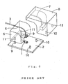
- the optical module disclosed in JP-A-2006-154553 includes a board 2 mounted with an optical element 1 such as a surface emitting element, and a receptacle which is capable of positioning a flexible optical waveguide 3 with respect to the optical element 1 with the optical axes of the flexible optical waveguide and the optical element 1 aligned with each other.
- an optical element 1 such as a surface emitting element
- a receptacle which is capable of positioning a flexible optical waveguide 3 with respect to the optical element 1 with the optical axes of the flexible optical waveguide and the optical element 1 aligned with each other.
- the receptacle includes a first receptacle 6 and a second receptacle 8 respectively having a lower groove 5 and an upper groove 7 which cooperatively serve as a guide for positioning the flexible optical waveguide 3.
- the first receptacle 6 and the second receptacle 8 are unitarily combined with each other by bringing guide pins 9 and 10 projecting upright from an upper surface of the board 2 into engagement with guide holes 11 and 12 formed in lower surfaces of the first and second receptacles 6 and 8, respectively.
- the production of the receptacle structure of the optical module requires a complicated process including the steps of preparing the first receptacle 6 and the second receptacle 8, and combining these two components with each other on the board 2.
- the optical element 1 and the flexible optical waveguide 3 are positioned with respect to each other via the combined receptacle structure, so that the overall accuracy is dependent upon the cumulative processing errors and the cumulative assembling errors of the respective components. This makes it difficult to control the accuracy.
- an optical waveguide device production method which includes the steps of: mounting a light emitting/receiving element on an upper surface of a board; enclosing the mounted light emitting/receiving element with a mold; filling a core material in the mold and curing the core material to form a core layer, whereby the light emitting/receiving element is sealed in the core layer and an optical waveguide insertion recess and an optical coupling lens are unitarily formed in a portion of the core layer opposed to a light emitting/receiving surface of the light emitting/receiving element; demolding the resulting product; and inserting one end of an optical waveguide into the optical waveguide insertion recess of the core layer, and fixing the one end of the optical waveguide in the optical waveguide insertion recess by sealing the one end of the optical waveguide with a resin.
- an optical waveguide device production method in which the mold is a transparent mold prepared by using at least one of quartz glass and silicon, and the mold is placed so that the optical coupling lens to be formed by the mold is centered coaxially with a light emitting/receiving point of the light emitting/receiving element while the inside of the mold is viewed through the mold in the optical waveguide device production method.
- an optical waveguide device production method in which the mold is a metal mold, and the mold and the board are respectively provided with alignment marks, which are aligned with each other so that the optical coupling lens to be formed by the mold is centered coaxially with the light emitting/receiving point of the light emitting/receiving element.
- an optical waveguide device produced by the production method according to the first aspect, the optical waveguide device including: a light emitting/receiving element mounted on an upper surface of a board; a core layer which seals the light emitting/receiving element, the core layer having an optical waveguide insertion recess and an optical coupling lens unitarily formed in a portion thereof opposed to a light emitting/receiving surface of the light emitting/receiving element; and an optical waveguide having one end inserted in the recess of the core layer and sealed with a resin to be fixed in the recess of the core layer, and optically coupled with a light emitting/receiving point of the light emitting/receiving element in the core layer.
- an optical waveguide connection structure to be used for the optical waveguide device according to the fourth aspect, the optical waveguide connection structure including a core layer which seals a light emitting/receiving element mounted on an upper surface of a board, the core layer having an optical waveguide insertion recess and an optical coupling lens unitarily formed in a portion thereof opposed to a light emitting/receiving surface of the light emitting/receiving element, wherein one end of an optical waveguide is inserted in the recess of the core layer and sealed with a resin to be fixed in the recess of the core layer, and the optical waveguide is optically coupled with the light emitting/receiving element in the core.
- the inventor of the present invention conducted intensive studies to provide a receptacle structure which ensures easy and highly accurate positioning of the light emitting/receiving element and the optical waveguide for optical coupling. As a result, the inventor found that the aforementioned object can be achieved by simultaneously forming the lens and the optical waveguide insertion recess required for the receptacle structure when the light emitting/receiving element is sealed with a resin for protection thereof from an external force. Thus, the inventor attained the present invention.
- the lens and the optical waveguide insertion recess required for the receptacle structure are simultaneously formed when the light emitting/receiving element is sealed with the resin for the protection of the element from the external force. Therefore, the receptacle structure can be easily and highly accurately produced in the single step.
- the optical waveguide device production method is advantageous in that production costs and time are significantly reduced without the need for the conventionally required complicated process.
- the mold is the transparent mold prepared by using at least one of quartz glass and silicon in the production method
- the mold is placed so that the optical coupling lens to be formed by the mold is centered coaxially with the light emitting/receiving point of the light emitting/receiving element while the inside of the mold is viewed through the mold.
- the production method is advantageous in that the centering is easily achieved when the mold is placed.
- the mold is the metal mold in the production method
- the mold and the board are respectively provided with the alignment marks, which are aligned with each other so that the optical coupling lens to be formed by the mold is centered coaxially with the light emitting/receiving point of the light emitting/receiving element.
- the production method is advantageous in that the centering is easily achieved when the mold is placed.
- the inventive optical waveguide device has a simplified structure with the light emitting/receiving element and the optical waveguide sealed in the core layer and yet the optical axes of the light emitting/receiving element and the optical waveguide are accurately aligned with each other for optical coupling. Therefore, the optical waveguide device can transmit high intensity light.
- the optical waveguide connection structure to be used for the optical waveguide device is advantageous in that easy and highly efficient transmission of light can be achieved at lower costs with a reduced light coupling loss.
- a production method for an optical waveguide device including a light emitting element and an optical waveguide optically coupled with each other will hereinafter be described by way of embodiment.
- a planar board 20 is first prepared, and a light emitting element 21 is mounted at a predetermined position on an upper surface of the board 20.
- Exemplary materials for the board 20 include glass, quartz glass, silicon, resins and metals.
- the thickness of the board 20 is properly determined according to the board material and the required properties of the board.
- the board 20 is a flexible printed circuit (FPC) board based on a polyester (PET) resin, a polycarbonate (PC) resin or a polyethylene naphthalate (PEN) resin, for example, the board 20 typically has a thickness of 30 to 300 ⁇ m.
- the board 20 is a rigid board based on a glass board or a quartz board, for example, the board 20 typically has a thickness of 1 to 5 mm.
- Examples of the light emitting element 21 include a light emitting diode (LED), a laser diode (LD) and a surface emitting laser (VCSEL).
- the light emitting element 21 is mounted on the board 20 by a wire bonding method or the like.
- the mold 22 has a ceiling surface 23 and side surfaces 24.
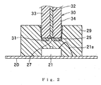
- the mold 22 has a projection 26 provided on a portion of the ceiling surface 23 opposed to a light emitting surface of the light emitting element 21 for forming an optical waveguide insertion recess 25 as shown in Fig. 1(b) , and a semispherical indentation 28 provided in a distal surface 26a of the projection 26 for forming an optical coupling lens 27 as shown in Fig. 1(b) .
- Exemplary materials for the mold 22 include metals, resins, silicon and quartz glass. Particularly, it is desirable that the mold 22 is a transparent mold such as of quartz glass or silicon. That is, active alignment can be achieved by viewing the light emitting element 21 from above through the transparent mold 22 to accurately position the mold 22 with respect to the light emitting element 21 so that the optical axis of the lens to be formed by the semispherical indentation 28 of the mold 22 is aligned with the optical axis of the light emitting element 21.
- the mold 22 and the board 20 are respectively provided with alignment marks, and active alignment is achieved by picking up an image of the alignment marks from a back side of the board 20.
- the mold 22 is directly engraved with the alignment mark and the board 20 is formed with the alignment mark by printing or Cu plating.
- the projection 26 of the mold 22 for forming the optical waveguide insertion recess 25 is configured such that the recess 25 to be formed has a tapered slit shape. Therefore, when a film-shaped optical waveguide 30 is inserted into the recess 25, as shown in Fig. 2 , the optical waveguide 30 is fitted in the recess 25 with tolerance. Even if the optical waveguide 30 has slight variations in thickness, the variations are accommodated by the light collecting effect of the lens 27 to be described later.
- the height H of the distal surface 26a of the projection 26 should be determined such that bonding wires 21a of the light emitting element 21 do not contact the distal surface 26a. This is because the distal surface 26a of the projection 26, if in contact with the bonding wires 21a, would press and break the bonding wires 21a.
- the mold 22 preferably has a height (internal height) of not greater than 10 mm, a width of not greater than about 20 mm and a length of not greater than about 20 mm.
- the height (H) of the distal surface 26a of the projection 26 is preferably not less than 400 ⁇ m for prevention of the contact with the bonding wires 21a.
- a core material is filled in the mold 22, and cured.
- a core layer 29 is formed, and then demolded.
- a molded product produced in this manner is such that the light emitting element 21 is sealed in the core layer 29, which has the optical waveguide insertion recess 25 formed in an upper portion thereof as having the tapered slit shape and the optical coupling lens 27 having the light collecting effect.
- the core material may be any of those commonly used for the optical waveguide.
- the core material include photosensitive resins such as photosensitive epoxy resins, photosensitive polyimide resins, photosensitive polyamide resins and photosensitive silicone resins, and thermosetting resins such as non-photosensitive epoxy resins and polyimide resins, which may be each used in the form of a varnish prepared by dissolving the resin in a solvent.
- photosensitive resins such as photosensitive epoxy resins, photosensitive polyimide resins, photosensitive polyamide resins and photosensitive silicone resins
- thermosetting resins such as non-photosensitive epoxy resins and polyimide resins, which may be each used in the form of a varnish prepared by dissolving the resin in a solvent.
- the photosensitive epoxy resins are preferred.
- the core material is typically cured through spot irradiation with ultraviolet radiation.
- the dose of the ultraviolet radiation is typically 100 to 5000 mJ/cm 2 , preferably 2000 to 3000 mJ/cm 2 .
- the irradiation period is 1 to 3 seconds.
- a thermosetting resin such as a polyimide resin
- the core material is typically cured through a heat treatment at 300 to 400°C for 60 to 180 minutes.
- a sealing resin material is injected into the optical waveguide insertion recess 25, and cured with the optical waveguide 30 being inserted in the recess 25.
- the optical waveguide 30 is fixed.
- a reference numeral 31 denotes the cured sealing resin.
- the sealing resin material may be any of cladding layer materials conventionally used for the optical waveguide.
- the sealing resin material include photosensitive resins such as photosensitive epoxy resins, photosensitive polyimide resins, photosensitive polyamide resins and photosensitive silicone resins, and thermosetting resins such as non-photosensitive epoxy resins and polyimide resins, which may be each used in the form of a varnish prepared by dissolving the resin in a solvent.
- photosensitive epoxy resins are preferred.
- the sealing resin 31 preferably has a lower refractive index than the core layer 29 in order to minimize the loss of light emitted through the core layer 29.
- the sealing resin material is typically cured through spot irradiation with ultraviolet radiation.
- the dose of the ultraviolet radiation is typically 100 to 5000 mJ/cm 2 , preferably 2000 to 3000 mJ/cm 2 .
- the irradiation period is 1 to 5 seconds.
- a thermosetting resin such as a polyimide resin
- the sealing resin material is typically cured through a heat treatment at 300 to 400°C for 60 to 180 minutes.
- the optical waveguide 30 to be inserted in the optical waveguide insertion recess 25 includes band-shaped films 33, 34 serving as cladding layers, and a longitudinally extending flexible core layer 32 sandwiched between the films 33, 34 and unitarily combined with the films 33, 34.
- a typical example of the optical waveguide is a laminate film including layers formed of a polyimide resin, a polyamide resin and/or an epoxy resin having refractive indexes properly adjusted.
- the optical waveguide preferably has an overall thickness of about 0.1 to about 2 mm.
- the optical waveguide device thus produced is capable of transmitting high intensity light, because the light emitting element 21 and the optical waveguide 30 are highly accurately positioned with respect to each other with the optical axes thereof aligned with each other for optical coupling.
- the optical waveguide device production method described above is practically effective, because the high quality optical waveguide device can be easily produced in a short time.
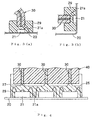
- the flexible film-shaped optical waveguide 30 is used. Therefore, the film-shaped optical waveguide 30 connected to the board 20 can be routed in any direction from a mounting surface of the board 20 as shown in Fig. 3(a) . Even if the optical waveguide 30 is not flexible, as shown in Fig. 3(b) , the optical waveguide 30 can be mounted in any desired orientation (in a vertical orientation in Fig. 3(b) ) by using a flexible FPC board as the board 20. By thus using flexible materials for at least one of the board 20 and the optical waveguide 30, the optical waveguide device can be mounted in any arrangement required for a given application.
- the single optical waveguide 30 is connected to the single light emitting element 21.
- a board 20 mounted with a plurality of light emitting elements 21 arranged at a predetermined pitch may be prepared, and a corresponding number of optical waveguides 30 bundled in parallel relation into an optical waveguide set 40 may be respectively connected to the light emitting elements 21.
- Fig. 4 is a sectional view taken along a sectional plane different by 90 degrees from the sectional plane in Fig. 2 .
- a sealing resin 31 (see Fig. 2 ) in optical waveguide insertion recesses 25 is not shown in Fig. 4 .
- the optical waveguide device is adapted to input light emitted from the light emitting element 21 into the core layer 32 of the film-shaped optical waveguide 30 for optical coupling.
- the optical waveguide device according to the present invention may be adapted to input light outputted from the core layer of the optical waveguide into a light receiving element for optical coupling.
- a glass mold was prepared, which was configured to allow the optical waveguide insertion recess to have an opening width of 1 mm and a bottom width of 0.15 mm and to allow the optical coupling lens to have a diameter of 0.1 mm.
- the mold was engraved with an alignment mark.
- a core material was prepared by dissolving 70 parts by weight of bisphenoxyethanolfluorene diglycidyl ether (Component A), 30 parts by weight of 1,3,3-tris ⁇ 4-[2-(3-oxetanyl)]butoxyphenyl ⁇ butane and 0.5 part by weight of a 50% propione carbonate solution of 4,4-bis[di( ⁇ -hydroxyethoxy)phenylsulfinio]phenylsulfide bishexafluoroantimonate (photoacid generator, Component B) in 28 parts by weight of ethyl lactate.
- a sealing resin material was prepared by mixing together 35 parts by weight of bisphenoxyethanolfluorene diglycidyl ether (component A), 40 parts by weight of 3',4'-epoxycyclohexylmethyl-3,4-epoxycyclohexane carboxylate which is an alicyclic epoxy resin (CELLOXIDE 2021P manufactured by Daicel Chemical Industries,Ltd.), 25 parts by weight of (3',4'-epoxycyclohexane)methyl-3',4'-epoxycyclohexyl-carboxylate(CELLOXIDE 2081 manufactured by Daicel Chemical Industries, Ltd.), and one part by weight of a 50% propione carbonate solution of 4,4-bis[di( ⁇ -hydroxyethoxy)phenylsulfinio] phenylsulfide-bis-hexafluoroantimonate (photo-acid generator: component B).
- a surface emitting laser (SM85-2N001 available from Optowell Co., Ltd.) was mounted as a light emitting element on an FPC board having a board thickness of 38 ⁇ m by connecting rear side terminals thereof to the board with the use of a silver paste and connecting front side terminals thereof to the board via Au (gold) wires each having a diameter of 25 ⁇ m through the wire bonding method at 110°C.
- the light emitting element mounted on the FPC board was enclosed with the mold, and the core material was filled in the mold. Then, the core material was cured through spot irradiation with ultraviolet radiation at 3000 mJ/cm 2 . Thus, a core layer of a receptacle structure was formed which sealed the light emitting element.
- the core layer was demolded.
- the sealing resin material was injected into the optical waveguide insertion recess of the core layer, one end of a film-shaped optical waveguide (having an overall thickness of 0.2 mm, a core layer thickness of 50 ⁇ m and a core layer width of 400 ⁇ m) was inserted into the optical waveguide insertion recess, and fixed in the optical waveguide insertion recess by curing the sealing resin material through spot irradiation with ultraviolet radiation at 3000 mJ/cm 2 .
- an optical waveguide device including the optical waveguide and the light emitting element optically coupled with each other via the receptacle structure was produced.
- the amount of light transmitted through the optical waveguide was 90% of that observed where the optical waveguide was fully centered coaxially with the light emitting element through the active alignment. Therefore, the optical waveguide device had high quality with a little light loss associated with the optical coupling.
Landscapes
- Physics & Mathematics (AREA)
- General Physics & Mathematics (AREA)
- Optics & Photonics (AREA)
- Engineering & Computer Science (AREA)
- Microelectronics & Electronic Packaging (AREA)
- Optical Couplings Of Light Guides (AREA)
- Optical Integrated Circuits (AREA)
- Led Device Packages (AREA)
- Light Receiving Elements (AREA)
Applications Claiming Priority (1)
| Application Number | Priority Date | Filing Date | Title |
|---|---|---|---|
| JP2007300594A JP4503064B2 (ja) | 2007-11-20 | 2007-11-20 | 光導波路デバイスの製法およびそれによって得られる光導波路デバイス、並びにそれに用いられる光導波路接続構造 |
Publications (2)
| Publication Number | Publication Date |
|---|---|
| EP2063302A1 true EP2063302A1 (fr) | 2009-05-27 |
| EP2063302B1 EP2063302B1 (fr) | 2016-04-06 |
Family
ID=40297709
Family Applications (1)
| Application Number | Title | Priority Date | Filing Date |
|---|---|---|---|
| EP08020117.1A Ceased EP2063302B1 (fr) | 2007-11-20 | 2008-11-18 | Procédé de production de dispositif de guide d'onde optique, guide d'onde optique produit par cette méthode, et structure de connexion d'un guide d'onde utilisée pour ce dispositif |
Country Status (5)
| Country | Link |
|---|---|
| US (1) | US7906355B2 (fr) |
| EP (1) | EP2063302B1 (fr) |
| JP (1) | JP4503064B2 (fr) |
| KR (1) | KR101510895B1 (fr) |
| CN (1) | CN101441298B (fr) |
Families Citing this family (14)
| Publication number | Priority date | Publication date | Assignee | Title |
|---|---|---|---|---|
| EP2246979A4 (fr) * | 2008-02-18 | 2014-03-05 | Murata Manufacturing Co | Dispositif à ondes élastiques et son procédé de fabrication |
| JP5402083B2 (ja) * | 2008-09-29 | 2014-01-29 | ソニー株式会社 | 固体撮像装置とその製造方法、及び電子機器 |
| JP5457913B2 (ja) * | 2010-03-31 | 2014-04-02 | ヒロセ電機株式会社 | 光モジュール装置及びその製造方法 |
| JP2012064719A (ja) * | 2010-09-15 | 2012-03-29 | Sumitomo Electric Ind Ltd | 光源装置、ディスプレイ装置 |
| TWI509300B (zh) * | 2011-12-14 | 2015-11-21 | Hon Hai Prec Ind Co Ltd | 光耦合模組及其製作方法 |
| JP5594316B2 (ja) * | 2012-05-11 | 2014-09-24 | 株式会社村田製作所 | 光伝送モジュール |
| JP2014197364A (ja) * | 2013-03-07 | 2014-10-16 | 日東電工株式会社 | 情報表示システム |
| KR101622469B1 (ko) * | 2013-07-05 | 2016-05-19 | 엘에스엠트론 주식회사 | 수동광정렬을 위한 옵티컬블럭을 구비하는 광모듈 및 그 제조방법 |
| JP6255237B2 (ja) * | 2013-12-25 | 2017-12-27 | 株式会社エンプラス | 光レセプタクルおよび光モジュール |
| JP6369936B2 (ja) | 2014-07-31 | 2018-08-08 | 日東電工株式会社 | 光センサ |
| KR20160067230A (ko) * | 2014-12-03 | 2016-06-14 | 엘에스엠트론 주식회사 | 광모듈의 광소자와 광전송부재 간의 광축정렬방법 |
| US9678289B1 (en) * | 2015-12-02 | 2017-06-13 | International Business Machines Corporation | Thermal management of optical coupling systems |
| GB2555398B (en) * | 2016-10-24 | 2020-04-08 | Toshiba Kk | An optoelectronic system and method for its fabrication |
| CN109567782B (zh) * | 2017-09-28 | 2022-03-11 | 陈右颖 | 结合有光波导的神经探针及其制造方法 |
Citations (10)
| Publication number | Priority date | Publication date | Assignee | Title |
|---|---|---|---|---|
| US4433898A (en) * | 1980-12-22 | 1984-02-28 | National Semiconductor Corporation | Fiber optic assembly for coupling an optical fiber and a light source |
| JPH042179A (ja) * | 1990-04-18 | 1992-01-07 | Honda Motor Co Ltd | 光リンクの製造方法 |
| GB2316225A (en) * | 1996-08-06 | 1998-02-18 | Northern Telecom Ltd | Semiconductor photodetector packaging |
| DE19711138A1 (de) * | 1997-03-07 | 1998-09-10 | Siemens Ag | Herstellungsverfahren für ein elektrooptisches Modul |
| EP1031860A2 (fr) * | 1999-02-22 | 2000-08-30 | Infineon Technologies AG | Méthode et moule pour la fabrication d'un module électro-optique et module électro-optique |
| US20030007749A1 (en) * | 2000-02-02 | 2003-01-09 | Hans Hurt | Electrooptical transmitting/receiving module, and method for producing the module |
| US20040061956A1 (en) * | 2002-03-08 | 2004-04-01 | Nikolaus Schunk | Receiving and coupling part for opto-electronic transmission and/or reception element |
| US20040085609A1 (en) * | 2002-10-29 | 2004-05-06 | Manfred Fries | Method for producing an optoelectronic component |
| JP2006154553A (ja) | 2004-11-30 | 2006-06-15 | Seiko Epson Corp | 光モジュール |
| DE102007044555A1 (de) * | 2007-07-18 | 2009-01-22 | Siemens Ag | Optische Koppelvorrichtung und Verfahren zu deren Herstellung |
Family Cites Families (15)
| Publication number | Priority date | Publication date | Assignee | Title |
|---|---|---|---|---|
| JPS5524404A (en) * | 1978-08-09 | 1980-02-21 | Toshiba Corp | Semiconductor light emitting device |
| JPS562263U (fr) * | 1979-06-18 | 1981-01-10 | ||
| US4941255A (en) * | 1989-11-15 | 1990-07-17 | Eastman Kodak Company | Method for precision multichip assembly |
| JPH10307237A (ja) * | 1997-05-08 | 1998-11-17 | New Japan Radio Co Ltd | 一体型光通信用半導体装置 |
| JP2000110176A (ja) | 1998-10-02 | 2000-04-18 | Fujitsu Ltd | 光モジュール及びその製造方法 |
| US6932516B2 (en) * | 2000-07-19 | 2005-08-23 | Canon Kabushiki Kaisha | Surface optical device apparatus, method of fabricating the same, and apparatus using the same |
| AUPR245701A0 (en) * | 2001-01-10 | 2001-02-01 | Silverbrook Research Pty Ltd | An apparatus (WSM10) |
| DE10151113B4 (de) * | 2001-10-15 | 2004-03-25 | Infineon Technologies Ag | Opto-elektronisches Modul und Verfahren zu seiner Herstellung |
| WO2004038473A1 (fr) * | 2002-10-22 | 2004-05-06 | Firecomms Limited | Connexion de guides d'ondes optiques a des dispositifs optiques |
| JP2005024617A (ja) * | 2003-06-30 | 2005-01-27 | Sharp Corp | 光送信器 |
| JP2005055796A (ja) * | 2003-08-07 | 2005-03-03 | Sanyo Electric Co Ltd | 反射防止部材を設けた光コネクタ及びその形成方法 |
| JP4180537B2 (ja) * | 2003-10-31 | 2008-11-12 | シャープ株式会社 | 光学素子の封止構造体および光結合器ならびに光学素子の封止方法 |
| US20060091418A1 (en) * | 2004-11-04 | 2006-05-04 | Chew Tong F | Side emitting LED device and method of fabrication |
| JP2006210297A (ja) | 2005-01-31 | 2006-08-10 | Tdk Corp | Elパネルの製造方法 |
| JP4768433B2 (ja) * | 2005-12-22 | 2011-09-07 | シャープ株式会社 | 光半導体装置およびそれを備えた電子機器 |
-
2007
- 2007-11-20 JP JP2007300594A patent/JP4503064B2/ja not_active Expired - Fee Related
-
2008
- 2008-11-18 EP EP08020117.1A patent/EP2063302B1/fr not_active Ceased
- 2008-11-18 US US12/273,084 patent/US7906355B2/en active Active
- 2008-11-19 KR KR20080115102A patent/KR101510895B1/ko not_active Expired - Fee Related
- 2008-11-20 CN CN2008101809747A patent/CN101441298B/zh active Active
Patent Citations (10)
| Publication number | Priority date | Publication date | Assignee | Title |
|---|---|---|---|---|
| US4433898A (en) * | 1980-12-22 | 1984-02-28 | National Semiconductor Corporation | Fiber optic assembly for coupling an optical fiber and a light source |
| JPH042179A (ja) * | 1990-04-18 | 1992-01-07 | Honda Motor Co Ltd | 光リンクの製造方法 |
| GB2316225A (en) * | 1996-08-06 | 1998-02-18 | Northern Telecom Ltd | Semiconductor photodetector packaging |
| DE19711138A1 (de) * | 1997-03-07 | 1998-09-10 | Siemens Ag | Herstellungsverfahren für ein elektrooptisches Modul |
| EP1031860A2 (fr) * | 1999-02-22 | 2000-08-30 | Infineon Technologies AG | Méthode et moule pour la fabrication d'un module électro-optique et module électro-optique |
| US20030007749A1 (en) * | 2000-02-02 | 2003-01-09 | Hans Hurt | Electrooptical transmitting/receiving module, and method for producing the module |
| US20040061956A1 (en) * | 2002-03-08 | 2004-04-01 | Nikolaus Schunk | Receiving and coupling part for opto-electronic transmission and/or reception element |
| US20040085609A1 (en) * | 2002-10-29 | 2004-05-06 | Manfred Fries | Method for producing an optoelectronic component |
| JP2006154553A (ja) | 2004-11-30 | 2006-06-15 | Seiko Epson Corp | 光モジュール |
| DE102007044555A1 (de) * | 2007-07-18 | 2009-01-22 | Siemens Ag | Optische Koppelvorrichtung und Verfahren zu deren Herstellung |
Also Published As
| Publication number | Publication date |
|---|---|
| JP2009128430A (ja) | 2009-06-11 |
| US7906355B2 (en) | 2011-03-15 |
| KR20090052286A (ko) | 2009-05-25 |
| CN101441298A (zh) | 2009-05-27 |
| CN101441298B (zh) | 2011-12-21 |
| US20090127577A1 (en) | 2009-05-21 |
| KR101510895B1 (ko) | 2015-04-10 |
| JP4503064B2 (ja) | 2010-07-14 |
| EP2063302B1 (fr) | 2016-04-06 |
Similar Documents
| Publication | Publication Date | Title |
|---|---|---|
| US7906355B2 (en) | Optical waveguide device production method, optical waveguide device produced by the method, and optical waveguide connection structure to be used for the device | |
| EP2598928B1 (fr) | Corps ayant une lentille couplée pour réaliser une image d'un élément d'alignement | |
| US7343060B2 (en) | Light transmission and reception module, sub-mount, and method of manufacturing the sub-mount | |
| US9952391B2 (en) | Optical transmission module, endoscope, and method for manufacturing optical transmission module | |
| US20080138007A1 (en) | Optical waveguide and optical module using the same | |
| US8388239B2 (en) | Manufacturing method of opto-electric hybrid module and opto-electric hybrid module manufactured thereby | |
| CN102636844A (zh) | 光连接器的制造方法 | |
| CN101852898B (zh) | 光连接器及使用了光连接器的光纤模块 | |
| US7627210B2 (en) | Manufacturing method of optical-electrical substrate and optical-electrical substrate | |
| JP2009198804A (ja) | 光モジュール及び光導波路 | |
| JP2012113177A (ja) | 光コネクタおよびその製法 | |
| KR20120021230A (ko) | 광 센서 모듈 | |
| JP4881329B2 (ja) | 光導波路デバイスの製法およびそれによって得られる光導波路デバイス、並びにそれに用いられる光導波路接続構造 | |
| JP2012189950A (ja) | 光電気混載基板およびその製法 | |
| KR20100055719A (ko) | 광전변환모듈 | |
| JP6015210B2 (ja) | 光導波路の位置合わせ方法および光配線部品の製造方法 | |
| JP2007072007A (ja) | 光導波路モジュール | |
| JP2006243467A (ja) | 光送受信モジュール | |
| JP2007178852A (ja) | 光配線基板及びこれを用いた光モジュール | |
| US20190219759A1 (en) | Optical waveguide | |
| JP2021113844A (ja) | 光配線部品の製造方法 | |
| US8606056B2 (en) | Opto-electric hybrid board and manufacturing method therefor | |
| EP1998199A1 (fr) | Couplage optique entre un élément d`emission de lumière et un coeur de guide d`ondes muni d`une ouverture au niveau de sa surface de réception de lumière | |
| JP2012032733A (ja) | 光モジュール及びその製造方法 |
Legal Events
| Date | Code | Title | Description |
|---|---|---|---|
| PUAI | Public reference made under article 153(3) epc to a published international application that has entered the european phase |
Free format text: ORIGINAL CODE: 0009012 |
|
| AK | Designated contracting states |
Kind code of ref document: A1 Designated state(s): AT BE BG CH CY CZ DE DK EE ES FI FR GB GR HR HU IE IS IT LI LT LU LV MC MT NL NO PL PT RO SE SI SK TR |
|
| AX | Request for extension of the european patent |
Extension state: AL BA MK RS |
|
| 17P | Request for examination filed |
Effective date: 20090922 |
|
| 17Q | First examination report despatched |
Effective date: 20091112 |
|
| AKX | Designation fees paid |
Designated state(s): DE GB |
|
| RBV | Designated contracting states (corrected) |
Designated state(s): DE GB |
|
| GRAP | Despatch of communication of intention to grant a patent |
Free format text: ORIGINAL CODE: EPIDOSNIGR1 |
|
| INTG | Intention to grant announced |
Effective date: 20151116 |
|
| GRAS | Grant fee paid |
Free format text: ORIGINAL CODE: EPIDOSNIGR3 |
|
| GRAA | (expected) grant |
Free format text: ORIGINAL CODE: 0009210 |
|
| INTG | Intention to grant announced |
Effective date: 20160211 |
|
| AK | Designated contracting states |
Kind code of ref document: B1 Designated state(s): DE GB |
|
| REG | Reference to a national code |
Ref country code: GB Ref legal event code: FG4D |
|
| REG | Reference to a national code |
Ref country code: DE Ref legal event code: R096 Ref document number: 602008043275 Country of ref document: DE |
|
| REG | Reference to a national code |
Ref country code: DE Ref legal event code: R097 Ref document number: 602008043275 Country of ref document: DE |
|
| PLBE | No opposition filed within time limit |
Free format text: ORIGINAL CODE: 0009261 |
|
| STAA | Information on the status of an ep patent application or granted ep patent |
Free format text: STATUS: NO OPPOSITION FILED WITHIN TIME LIMIT |
|
| 26N | No opposition filed |
Effective date: 20170110 |
|
| REG | Reference to a national code |
Ref country code: DE Ref legal event code: R119 Ref document number: 602008043275 Country of ref document: DE |
|
| GBPC | Gb: european patent ceased through non-payment of renewal fee |
Effective date: 20161118 |
|
| PG25 | Lapsed in a contracting state [announced via postgrant information from national office to epo] |
Ref country code: GB Free format text: LAPSE BECAUSE OF NON-PAYMENT OF DUE FEES Effective date: 20161118 Ref country code: DE Free format text: LAPSE BECAUSE OF NON-PAYMENT OF DUE FEES Effective date: 20170601 |