EP2065941A2 - Solarzelle und Herstellungsverfahren dafür - Google Patents
Solarzelle und Herstellungsverfahren dafür Download PDFInfo
- Publication number
- EP2065941A2 EP2065941A2 EP08253855A EP08253855A EP2065941A2 EP 2065941 A2 EP2065941 A2 EP 2065941A2 EP 08253855 A EP08253855 A EP 08253855A EP 08253855 A EP08253855 A EP 08253855A EP 2065941 A2 EP2065941 A2 EP 2065941A2
- Authority
- EP
- European Patent Office
- Prior art keywords
- solar cell
- holes
- main surface
- light
- receiving surface
- Prior art date
- Legal status (The legal status is an assumption and is not a legal conclusion. Google has not performed a legal analysis and makes no representation as to the accuracy of the status listed.)
- Withdrawn
Links
- 238000004519 manufacturing process Methods 0.000 title claims abstract description 20
- 238000005530 etching Methods 0.000 claims abstract description 126
- 239000000758 substrate Substances 0.000 claims description 94
- 229910021419 crystalline silicon Inorganic materials 0.000 claims description 74
- 239000004065 semiconductor Substances 0.000 claims description 70
- 239000000969 carrier Substances 0.000 claims description 14
- 230000000149 penetrating effect Effects 0.000 claims description 12
- 238000000034 method Methods 0.000 abstract description 105
- JBJWASZNUJCEKT-UHFFFAOYSA-M sodium;hydroxide;hydrate Chemical compound O.[OH-].[Na+] JBJWASZNUJCEKT-UHFFFAOYSA-M 0.000 abstract description 10
- 229910021417 amorphous silicon Inorganic materials 0.000 description 44
- 229910021420 polycrystalline silicon Inorganic materials 0.000 description 26
- 238000006243 chemical reaction Methods 0.000 description 24
- 238000005229 chemical vapour deposition Methods 0.000 description 19
- XUIMIQQOPSSXEZ-UHFFFAOYSA-N Silicon Chemical compound [Si] XUIMIQQOPSSXEZ-UHFFFAOYSA-N 0.000 description 15
- 230000015572 biosynthetic process Effects 0.000 description 15
- 229910052710 silicon Inorganic materials 0.000 description 15
- 239000010703 silicon Substances 0.000 description 15
- KRHYYFGTRYWZRS-UHFFFAOYSA-N Fluorane Chemical compound F KRHYYFGTRYWZRS-UHFFFAOYSA-N 0.000 description 12
- 230000001681 protective effect Effects 0.000 description 10
- GRYLNZFGIOXLOG-UHFFFAOYSA-N Nitric acid Chemical compound O[N+]([O-])=O GRYLNZFGIOXLOG-UHFFFAOYSA-N 0.000 description 8
- 229910017604 nitric acid Inorganic materials 0.000 description 8
- 238000007740 vapor deposition Methods 0.000 description 8
- 239000010408 film Substances 0.000 description 7
- 229920002120 photoresistant polymer Polymers 0.000 description 7
- 238000007789 sealing Methods 0.000 description 7
- HEMHJVSKTPXQMS-UHFFFAOYSA-M Sodium hydroxide Chemical compound [OH-].[Na+] HEMHJVSKTPXQMS-UHFFFAOYSA-M 0.000 description 6
- 230000000694 effects Effects 0.000 description 6
- 238000005240 physical vapour deposition Methods 0.000 description 6
- 229920001187 thermosetting polymer Polymers 0.000 description 6
- 239000004020 conductor Substances 0.000 description 5
- 238000007650 screen-printing Methods 0.000 description 5
- 230000008901 benefit Effects 0.000 description 4
- 238000009792 diffusion process Methods 0.000 description 4
- 239000012535 impurity Substances 0.000 description 4
- 238000002156 mixing Methods 0.000 description 4
- QPJSUIGXIBEQAC-UHFFFAOYSA-N n-(2,4-dichloro-5-propan-2-yloxyphenyl)acetamide Chemical compound CC(C)OC1=CC(NC(C)=O)=C(Cl)C=C1Cl QPJSUIGXIBEQAC-UHFFFAOYSA-N 0.000 description 4
- 150000002823 nitrates Chemical class 0.000 description 4
- -1 polyethylene terephthalate Polymers 0.000 description 4
- 229920005989 resin Polymers 0.000 description 3
- 239000011347 resin Substances 0.000 description 3
- RYGMFSIKBFXOCR-UHFFFAOYSA-N Copper Chemical compound [Cu] RYGMFSIKBFXOCR-UHFFFAOYSA-N 0.000 description 2
- VYPSYNLAJGMNEJ-UHFFFAOYSA-N Silicium dioxide Chemical compound O=[Si]=O VYPSYNLAJGMNEJ-UHFFFAOYSA-N 0.000 description 2
- 239000011248 coating agent Substances 0.000 description 2
- 238000000576 coating method Methods 0.000 description 2
- 229910052802 copper Inorganic materials 0.000 description 2
- 239000010949 copper Substances 0.000 description 2
- 238000007733 ion plating Methods 0.000 description 2
- 229920000139 polyethylene terephthalate Polymers 0.000 description 2
- 239000005020 polyethylene terephthalate Substances 0.000 description 2
- 239000012808 vapor phase Substances 0.000 description 2
- 238000012935 Averaging Methods 0.000 description 1
- JOYRKODLDBILNP-UHFFFAOYSA-N Ethyl urethane Chemical compound CCOC(N)=O JOYRKODLDBILNP-UHFFFAOYSA-N 0.000 description 1
- 239000004698 Polyethylene Substances 0.000 description 1
- 239000004743 Polypropylene Substances 0.000 description 1
- BQCADISMDOOEFD-UHFFFAOYSA-N Silver Chemical compound [Ag] BQCADISMDOOEFD-UHFFFAOYSA-N 0.000 description 1
- 239000011230 binding agent Substances 0.000 description 1
- 229910052681 coesite Inorganic materials 0.000 description 1
- 239000000470 constituent Substances 0.000 description 1
- 229910052906 cristobalite Inorganic materials 0.000 description 1
- 230000005684 electric field Effects 0.000 description 1
- 230000005611 electricity Effects 0.000 description 1
- 239000003822 epoxy resin Substances 0.000 description 1
- 230000005496 eutectics Effects 0.000 description 1
- 239000011888 foil Substances 0.000 description 1
- 239000011521 glass Substances 0.000 description 1
- LNEPOXFFQSENCJ-UHFFFAOYSA-N haloperidol Chemical compound C1CC(O)(C=2C=CC(Cl)=CC=2)CCN1CCCC(=O)C1=CC=C(F)C=C1 LNEPOXFFQSENCJ-UHFFFAOYSA-N 0.000 description 1
- 229910052738 indium Inorganic materials 0.000 description 1
- 238000012986 modification Methods 0.000 description 1
- 230000004048 modification Effects 0.000 description 1
- 229910021421 monocrystalline silicon Inorganic materials 0.000 description 1
- 229920003023 plastic Polymers 0.000 description 1
- 229920000647 polyepoxide Polymers 0.000 description 1
- 229920000573 polyethylene Polymers 0.000 description 1
- 229920005672 polyolefin resin Polymers 0.000 description 1
- 229920001155 polypropylene Polymers 0.000 description 1
- 229920001296 polysiloxane Polymers 0.000 description 1
- 238000007639 printing Methods 0.000 description 1
- 239000000377 silicon dioxide Substances 0.000 description 1
- 229910052709 silver Inorganic materials 0.000 description 1
- 239000004332 silver Substances 0.000 description 1
- 238000005245 sintering Methods 0.000 description 1
- 229910000679 solder Inorganic materials 0.000 description 1
- 229910052682 stishovite Inorganic materials 0.000 description 1
- 239000010409 thin film Substances 0.000 description 1
- 229910052718 tin Inorganic materials 0.000 description 1
- 229910052719 titanium Inorganic materials 0.000 description 1
- 229910052905 tridymite Inorganic materials 0.000 description 1
- 229910052721 tungsten Inorganic materials 0.000 description 1
- 229910052725 zinc Inorganic materials 0.000 description 1
Images




Classifications
-
- H—ELECTRICITY
- H10—SEMICONDUCTOR DEVICES; ELECTRIC SOLID-STATE DEVICES NOT OTHERWISE PROVIDED FOR
- H10F—INORGANIC SEMICONDUCTOR DEVICES SENSITIVE TO INFRARED RADIATION, LIGHT, ELECTROMAGNETIC RADIATION OF SHORTER WAVELENGTH OR CORPUSCULAR RADIATION
- H10F77/00—Constructional details of devices covered by this subclass
- H10F77/20—Electrodes
- H10F77/206—Electrodes for devices having potential barriers
- H10F77/211—Electrodes for devices having potential barriers for photovoltaic cells
- H10F77/219—Arrangements for electrodes of back-contact photovoltaic cells
- H10F77/223—Arrangements for electrodes of back-contact photovoltaic cells for metallisation wrap-through [MWT] photovoltaic cells
-
- H—ELECTRICITY
- H10—SEMICONDUCTOR DEVICES; ELECTRIC SOLID-STATE DEVICES NOT OTHERWISE PROVIDED FOR
- H10F—INORGANIC SEMICONDUCTOR DEVICES SENSITIVE TO INFRARED RADIATION, LIGHT, ELECTROMAGNETIC RADIATION OF SHORTER WAVELENGTH OR CORPUSCULAR RADIATION
- H10F10/00—Individual photovoltaic cells, e.g. solar cells
- H10F10/10—Individual photovoltaic cells, e.g. solar cells having potential barriers
- H10F10/16—Photovoltaic cells having only PN heterojunction potential barriers
- H10F10/164—Photovoltaic cells having only PN heterojunction potential barriers comprising heterojunctions with Group IV materials, e.g. ITO/Si or GaAs/SiGe photovoltaic cells
- H10F10/165—Photovoltaic cells having only PN heterojunction potential barriers comprising heterojunctions with Group IV materials, e.g. ITO/Si or GaAs/SiGe photovoltaic cells the heterojunctions being Group IV-IV heterojunctions, e.g. Si/Ge, SiGe/Si or Si/SiC photovoltaic cells
- H10F10/166—Photovoltaic cells having only PN heterojunction potential barriers comprising heterojunctions with Group IV materials, e.g. ITO/Si or GaAs/SiGe photovoltaic cells the heterojunctions being Group IV-IV heterojunctions, e.g. Si/Ge, SiGe/Si or Si/SiC photovoltaic cells the Group IV-IV heterojunctions being heterojunctions of crystalline and amorphous materials, e.g. silicon heterojunction [SHJ] photovoltaic cells
-
- H—ELECTRICITY
- H10—SEMICONDUCTOR DEVICES; ELECTRIC SOLID-STATE DEVICES NOT OTHERWISE PROVIDED FOR
- H10F—INORGANIC SEMICONDUCTOR DEVICES SENSITIVE TO INFRARED RADIATION, LIGHT, ELECTROMAGNETIC RADIATION OF SHORTER WAVELENGTH OR CORPUSCULAR RADIATION
- H10F10/00—Individual photovoltaic cells, e.g. solar cells
- H10F10/10—Individual photovoltaic cells, e.g. solar cells having potential barriers
- H10F10/17—Photovoltaic cells having only PIN junction potential barriers
- H10F10/174—Photovoltaic cells having only PIN junction potential barriers comprising monocrystalline or polycrystalline materials
-
- H—ELECTRICITY
- H10—SEMICONDUCTOR DEVICES; ELECTRIC SOLID-STATE DEVICES NOT OTHERWISE PROVIDED FOR
- H10F—INORGANIC SEMICONDUCTOR DEVICES SENSITIVE TO INFRARED RADIATION, LIGHT, ELECTROMAGNETIC RADIATION OF SHORTER WAVELENGTH OR CORPUSCULAR RADIATION
- H10F77/00—Constructional details of devices covered by this subclass
- H10F77/10—Semiconductor bodies
- H10F77/16—Material structures, e.g. crystalline structures, film structures or crystal plane orientations
- H10F77/162—Non-monocrystalline materials, e.g. semiconductor particles embedded in insulating materials
- H10F77/166—Amorphous semiconductors
- H10F77/1662—Amorphous semiconductors including only Group IV materials
-
- H—ELECTRICITY
- H10—SEMICONDUCTOR DEVICES; ELECTRIC SOLID-STATE DEVICES NOT OTHERWISE PROVIDED FOR
- H10F—INORGANIC SEMICONDUCTOR DEVICES SENSITIVE TO INFRARED RADIATION, LIGHT, ELECTROMAGNETIC RADIATION OF SHORTER WAVELENGTH OR CORPUSCULAR RADIATION
- H10F77/00—Constructional details of devices covered by this subclass
- H10F77/70—Surface textures, e.g. pyramid structures
- H10F77/703—Surface textures, e.g. pyramid structures of the semiconductor bodies, e.g. textured active layers
-
- Y—GENERAL TAGGING OF NEW TECHNOLOGICAL DEVELOPMENTS; GENERAL TAGGING OF CROSS-SECTIONAL TECHNOLOGIES SPANNING OVER SEVERAL SECTIONS OF THE IPC; TECHNICAL SUBJECTS COVERED BY FORMER USPC CROSS-REFERENCE ART COLLECTIONS [XRACs] AND DIGESTS
- Y02—TECHNOLOGIES OR APPLICATIONS FOR MITIGATION OR ADAPTATION AGAINST CLIMATE CHANGE
- Y02E—REDUCTION OF GREENHOUSE GAS [GHG] EMISSIONS, RELATED TO ENERGY GENERATION, TRANSMISSION OR DISTRIBUTION
- Y02E10/00—Energy generation through renewable energy sources
- Y02E10/50—Photovoltaic [PV] energy
- Y02E10/546—Polycrystalline silicon PV cells
-
- Y—GENERAL TAGGING OF NEW TECHNOLOGICAL DEVELOPMENTS; GENERAL TAGGING OF CROSS-SECTIONAL TECHNOLOGIES SPANNING OVER SEVERAL SECTIONS OF THE IPC; TECHNICAL SUBJECTS COVERED BY FORMER USPC CROSS-REFERENCE ART COLLECTIONS [XRACs] AND DIGESTS
- Y02—TECHNOLOGIES OR APPLICATIONS FOR MITIGATION OR ADAPTATION AGAINST CLIMATE CHANGE
- Y02E—REDUCTION OF GREENHOUSE GAS [GHG] EMISSIONS, RELATED TO ENERGY GENERATION, TRANSMISSION OR DISTRIBUTION
- Y02E10/00—Energy generation through renewable energy sources
- Y02E10/50—Photovoltaic [PV] energy
- Y02E10/548—Amorphous silicon PV cells
Definitions
- the present invention relates to a solar cell provided with a through hole electrode, and a manufacturing method of such solar cell.
- a solar cell can directly convert the clean and inexhaustibly supplied sunlight to electricity, and thus is expected as a new energy source.
- Such a solar cell has a plurality of through holes each penetrating the substrate from the light-receiving surface to the back surface. Photogenerated carriers collected on the light-receiving surface side of the substrate are conducted via a through hole electrode provided in a through hole to the back surface side of the solar cell. An insulating layer is formed on the inner wall surface of the through hole to prevent occurrence of a short circuit between the inner wall surface of the through hole and the through hole electrode.
- the through hole is formed by a laser processing or a mechanical processing, and consequently causes damages on its inner wall surface.
- the damage on the inner wall surface of the through hole is removed by an etching processing.
- a relief structure i.e., a so-called textured structure
- a textured structure is formed by an etching processing.
- the damage on the inner wall surface of the through hole can be removed by performing an etching processing on the inner wall surface simultaneously with performing an etching processing on the light-receiving surface for forming the textured structure after the formation of the through hole.
- a first aspect of the present invention is summarized as a solar cell including a semiconductor substrate having a first conductive type and including a first main surface and a second main surface; a semiconductor region having a second conductive type and provided on the first main surface of the semiconductor substrate; a plurality of through holes each provided in a plurality of portions in the semiconductor substrate and each penetrating from the first main surface to the second main surface; a plurality of through hole electrodes each provided in each of the plurality of through holes and each conducting photogenerated carriers collected in the semiconductor region to the second main surface side; and an insulating layer provided between an inner wall surface of each of the plurality of through holes and each of the plurality of through hole electrodes, wherein at least a part of the inner wall surface of each of the plurality of through holes is formed to be smoother compared to the first main surface of the semiconductor substrate,
- the first main surface of the semiconductor substrate and the inner wall surface of each of the plurality of through holes may be etched surfaces. Further, the first main surface of the semiconductor substrate may be a textured surface.
- At least a part of the inner wall surface of each of the plurality of through holes may have an arithmetic mean roughness smaller than an arithmetic mean roughness of the first main surface of the semiconductor substrate.
- the first main surface of the semiconductor substrate may be a textured surface
- the inner wall surface of each of the plurality of through holes may be an etched surface.
- the semiconductor substrate may be formed of single-crystalline silicon, the first main surface of the semiconductor substrate may be a (100) plane, and the inner wall surface of each of the plurality of through holes may be a (110) plane.
- the first aspect of the present invention may further include a plurality of first collective electrodes each formed on a surface of the semiconductor region and each collecting photogenerated carriers collected in the semiconductor region.
- each of the plurality of through hole electrodes may be electrically connected to each of the plurality of first collective electrodes.
- each of the plurality of through hole electrodes may be integrally formed with each of the plurality of first collective electrode.
- the first aspect of the present invention may further include a plurality of second collective electrodes each formed on the second main surface of the semiconductor substrate and each electrically connected to each of the plurality of through hole electrodes.
- the semiconductor region may be formed of amorphous semiconductor.
- the first main surface may be a light-receiving surface
- the second main surface may be a back surface
- a second aspect of the present invention is summarized as a manufacturing method of a solar cell, including: forming a plurality of through holes that penetrates from a first main surface to a second main surface of a semiconductor substrate having a first conductive type; etching an inner wall surface of each of the plurality of through holes; etching the first main surface of the semiconductor substrate; forming a semiconductor region on the first main surface of the semiconductor substrate; forming each of an insulating layer on the inner wall surface of each of the plurality of through holes; and forming each of a plurality of through hole electrodes in each of the plurality of through holes, wherein the inner wall surface of each of the plurality of through holes is etched to be smoother compared to the first main surface of the semiconductor substrate.
- the etching of the inner wall surface may be carried out by using a first etching solution
- the etching of the first main surface may be carried out by using a second etching solution
- an etching performance of the first etching solution may be higher than an etching performance of the second etching solution
- each of the plurality of through holes may be covered with a mask.
- the semiconductor substrate may be formed of single-crystalline silicon
- the first main surface of the semiconductor substrate may be a (100) plane
- a (110) plane may be exposed on at least a part of the inner wall surface of each of the plurality of through holes.
- the semiconductor region may be formed of amorphous semiconductor.
- Fig. 1 is a side view showing the configuration of a solar cell module 100 according to the embodiment.
- a solar cell module 100 includes a plurality of solar cells 1, a light-receiving-side protective member 2, a back-surface-side protective member 3, a sealing member 4, and a wiring member 5.
- the solar cell module 100 is formed by sealing a plurality of solar cells 1 between the light-receiving-side protective member 2 and the back-surface-side protective member 3 by using the sealing member 4.
- the plurality of solar cells 1 is arranged in an arrangement direction.
- the plurality of solar cells 1 is electrically connected to each other through the wiring member 5.
- Each solar cell 1 has a light-receiving surface (upper surface in Fig.1 ) for receiving the sunlight, and a back surface (lower surface in Fig.1 ) provided opposite to the light-receiving surface.
- the light-receiving surface and the back surface are main surfaces of the solar cell 1. The configuration of each of the solar cell 1 will be described hereinafter.
- the wiring member 5 is disposed on the back surface of the solar cell 1, and electrically connects one solar cell 1 to a different solar cell 1 adjacent to the one solar cell 1.
- the solar cell module 100 is a so-called a "back contact type" solar cell module.
- a conductive material such as copper, which is formed either into a thin-ptate shape or into a twisted-wire shape, may be used.
- eutectic solder may be plated.
- the light-receiving surface-side protective member 2 is provided on a light-receiving surface of the sealing member 4 and protects an upper surface of the solar cell module 10.
- a glass having transparent and water-blocking properties, transparent plastic, and the like may be used as the light-receiving surface-side protective member 2.
- the back-surface-side protective member 3 is provided on the back surface of the sealing member 4, and protects a back surface of the solar cell module 10.
- a resin film such as a PET (polyethylene terephthalate) film or a laminated film having a structure in which an AI foil is sandwiched therebetween, may be used.
- the sealing member 4 seals the plurality of solar cells 1 between the light-receiving surface-side protective member 2 and the back-surface-side protective member 3.
- resins including olefin resins such as polyethylene and polypropylene, and other resins such as EVA. EEA, PVB, silicone, urethane, acryl and epoxy resins may be used as the sealing member 4.
- an AI frame (not shown) may be attached to an outer circumference of the solar cell module 100 having the above-described configuration.
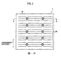
- Fig. 2 is a plan view of the solar cell 1 viewed from the light-receiving surface-side.
- Fig. 3 is a plan view of the solar cell 1 viewed from the back-surface-side.
- the solar cell 1 includes a photoelectric conversion part 10, a light-receiving surface-side collective electrode 24 and a through hole electrode 20.
- the photoelectric conversion part 10 has a light-receiving surface for receiving lights, and a back surface provided opposite to the light-receiving surface.
- the photoelectric conversion part 10 generates photogenerated carriers by use of the light received on the light-receiving surface.
- the photogenerated carriers are referred to electron holes and electrons generated by the solar light absorbed by the photoelectric conversion part 10.
- the photoelectric conversion part 10 has a structure called an HIT structure in which a substantially intrinsic amorphous silicon layer is interposed between a single crystalline silicon (semiconductor substrate) and an amorphous silicon layer (semiconductor region).
- the light-receiving surface-side collective electrode 24 is an electrode for collecting photogenerated carriers generated by the photoelectric conversion part 10.
- multiple light-receiving surface-side collective electrodes 24 are formed substantially on the entire area on the light-receiving surface of the photoelectric conversion part 10.
- the number of the light-receiving surface-side collective electrodes 24 can be modified appropriately in consideration of the size or the like of the photoelectric conversion part 10.
- the light-receiving surface-side collective electrode 24 can be formed by use of a printing method using a thermosetting conductive paste, for example.
- the through hole 20 is electrically connected to the light-receiving surface-side collective electrode 24, on the light-receiving surface of the photoelectric conversion part 10.
- the photogenerated carriers collected by the light-receiving surface-side collective electrode 24 from the photoelectric conversion part 10 are thereafter collected by the through hole electrode 20.
- the plurality of through hole electrodes 20 is provided in a plurality of portions. Further, each of the plurality of through hole electrodes 20 is provided in each of the through holes (not shown in Fig. 2 ,refer to Fig. 4 ) that is penetrating from the light-receiving surface to the back surface.
- the photoelectric conversion part 10 has ten through hole electrodes 20, in a row of five through hole electrodes 20 along the arrangement direction (see Fig.2 ).
- the number of the through hole electrodes 20 is modified appropriately in consideration of the number of the light-receiving surface-side collective electrodes 24, resistance ratio of the conductive material composing each of the through hole electrodes 20, and the like.
- the through hole electrodes 20 can be made of a conductive material similar to the light-receiving surface-side collective electrodes 24.
- the solar cell 1 further includes a light-receiving surface-side bus bar electrode 25 and a back-surface-side collective electrode 30.
- the light-receiving surface-side bus bar electrode 25 is an electrode for collecting photogenerated carriers from the five through hole electrodes 20 arranged in a row along the arrangement direction on the back surface of the photoelectric conversion part 10. As shown in Fig. 3 , the light-receiving surface-side bus bar electrodes 25 are formed in a line along the arrangement direction.
- the light-receiving surface-side bus bar electrode 25 is insulated from the back-surface-side of the photoelectric conversion part 10 and the back-surface-side collective electrode 30 by an insulating layer 17 described hereinafter.
- the light-receiving surface-side bus bar electrode 25 can be made of a conductive material similar to the light-receiving surface-side collective electrodes 24.
- the back-surface-side collective electrode 30 collects, from the photoelectric conversion part 10, photogenerated carriers having a different polarity from the photogenerated carriers collected by the light-receiving surface-side bus bar electrode 25.
- the back-surface-side collective electrode 30 is formed on the back surface of the photoelectric conversion part 10 in an area where the light-receiving surface-side bus bar electrode 25 is not formed.
- the present invention is not to limit the shape and the like of the collective electrode formed on the back surface of the photoelectric conversion part 10.
- a wiring member 5 is electrically connected to the light-receiving surface-side bus bar electrode 25 of one solar cell 1 and to the back-surface-side collective electrode 30 of a different solar cell 1 adjacent to the one solar cell 1.
- one end of the wiring member 5 is disposed on the light-receiving surface-side bus bar electrode 25 along the arrangement direction.
- the other end of the wiring member 5 is disposed on an end, in the arrangement direction, of the back-surface-side collective electrode 30.
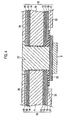
- Fig. 4 is an enlarged cross-sectional view taken along line A-A of Fig. 2 .
- the photoelectric conversion part 10 includes an n-type single-crystalline silicon 11, an i-type amorphous silicon layer 12, an n-type amorphous silicon layer 13, an i-type amorphous silicon layer 14, a p-type amorphous silicon layer 15, a back-surface-side transparent conductive layer 16, an insulating layer 17, and a light-receiving surface-side transparent conductive layer 18.
- the n-type single-crystalline silicon 11 contains single crystal silicon as a major component and has a thickness of about 200 ⁇ m.
- the n-type single-crystalline silicon 11 has a light-receiving surface, a back surface provided opposite to the light-receiving surface, a plurality of through holes each penetrating from the light-receiving surface to the back surface of the n-type single-crystalline silicon 11.
- a through hole electrode 20 is provided inside the through hole.
- the inner wall surface of the through hole is an etched surface formed by an etching processing.
- the light-receiving surface and the back surface of the n-type single-crystalline silicon 11 are a textured surface on which a fine textured structure (pyramid-like relief structure) is formed.
- Each of the texture has a height of several ⁇ m to several tens ⁇ m.
- the i-type amorphous silicon layer 12 is formed on the back surface of the n-type single-crystalline silicon 11.
- the i-type amorphous silicon layer 12 has a thickness of about 5 nm and is substantially intrinsic.
- the n-type amorphous silicon layer 13 is formed on the back surface of the i-type amorphous silicon layer 12 by use of a CVD method.
- the n-type amorphous silicon layer 13 has a thickness of about 5 nm.
- the n-type single-crystalline silicon 11, the i-type amorphous silicon layer 12 and the n-type amorphous silicon layer 13 form a so-called BSF structure.
- An i-type amorphous silicon layer 14 is formed on the light-receiving surface of the n-type single-crystalline silicon 11.
- the i-type amorphous silicon layer 14 has a thickness of about 5 nm and is substantially intrinsic.
- a p-type amorphous silicon layer 15 is formed on the back surface of the i-type amorphous silicon layer 14 by use of a CVD method.
- the p-type amorphous silicon layer 15 has a thickness of about 5 nm.
- a semiconductor junction that generates an electric field is formed by the n-type single-crystalline silicon 11, the i-type amorphous silicon layer 14 and the p-type amorphous silicon layer 15.
- a back-surface-side transparent conductive layer 16 is formed on the back surface of the n-type amorphous silicon layer 13 by use of a PVD method such as a spattering method and a vapor deposition method.
- the back-surface-side transparent conductive layer 16 can be formed of an oxide such as In, Zn, Sn, Ti and W.
- An insulating layer 17 is provided between the inner wall surface of the through hole, which is formed in the n-type single-crystalline silicon 11, and the through hole electrode 20, while extending from the inner wall surface to the back surface of the back-surface-side transparent conductive layer 16.
- the insulating layer 17 insulates the n-type single-crystalline silicon 11, the i-type amorphous silicon layer 12, the n-type amorphous silicon layer 13 and the back-surface-side transparent conductive layer 16 from the through hole electrode 20.
- the insulating layer 17 insulates the light-receiving surface-side bus bar electrode 25 from the back-surface-side collective electrode 30.
- the insulating layer 17 can be formed of, for example, SiN.
- a light-receiving surface-side transparent conductive layer 18 is formed on the light-receiving surface of the p-type amorphous silicon layer 15 by use of a PVD method such as a spattering method or a vapor deposition method.
- the light-receiving surface-side transparent conductive layer 18 can be made of a conductive material similar to the back-surface-side transparent conductive layer 16.
- Fig. 5 is a perspective view of the n-type single-crystalline silicon 11 according to the present embodiment viewed from the light-receiving surface-side.
- a textured structure is formed (in Fig.5 , only light-receiving surface is shown).
- Each of the textured structure has a height of several ⁇ m to several tens ⁇ m in a direction vertical to the light-receiving surface.
- the through holes each penetrating from the light-receiving surface to the back surface are formed.
- Each of the through holes is formed in a circle in a plan view of the n-type single-crystalline silicon 11.
- the inner wall surface of the through hole is formed by a uniformly smooth surface A.
- a relief structure (not shown) is formed on the uniformly smooth surface A.
- the relief structure formed on the uniformly smooth surface A is smaller and gentler than that of the textured structure formed on the light-receiving surface.
- Such a relief structure has a height (zero point several ⁇ m to several ⁇ m) of about one-tenth of that of the textured structure on the light-receiving surface.
- the inner wall surface of the through hole is formed to be smoother compared to the light-receiving surface.
- the arithmetic mean roughness (Ra) of the smooth surface A forming the inner wall surface of the through hole is smaller than the arithmetic mean roughness (Ra) of the light-receiving surface.
- the arithmetic mean roughness (Ra) is specified in conformity with Japanese Industrial Standard (JIS B 0601-1994).
- a manufacturing method of a solar cell 1 according to the present embodiment will be described hereinbelow.
- a manufacturing method of a solar cell 1 according to the present embodiment includes a first etching process in which the inner wall surface of the through hole is anisotropically etched, and a second etching process in which the light-receiving surface is anisotropically etched.
- the first etching process the inner wall surface of the through hole is formed to be smoother compared to the light-receiving surface.
- the first etching process uses a high concentration NaOH solution (5% by weight) and the second etching process uses a low concentration NaOH solution (1.5% by weight).
- the etching processes can be respectively performed under different conditions, on the inner wall surface of the through hole and on the light-receiving surface. Therefore, suitable etching processes for both of the inner wall surface and the light-receiving surface can be respectively performed.
- an etching rate is increased with relatively high concentration of the etching solution, so that an over-etched state is created.
- a gentle relief structure having a height of zero point several ⁇ m to several ⁇ m is formed on the inner wall surface of the through hole.
- a textured structure each having a height of several ⁇ m to several tens ⁇ m suitable for a solar cell is formed.
- the through hole is covered with an anti-etching mask in the second etching process. Therefore, it is possible to prevent the relief structure from being formed on the inner wall surface of the through hole in the second etching process.
- the smooth surface A having arithmetic mean roughness smaller than that of the light-receiving surface is formed.
- the insulating layer 17 can be formed to have uniform thickness. Accordingly, between the n-type single-crystalline silicon 11 and the through hole electrode 20 on the smooth surface A, occurrence of the short circuit can be suppressed. As a result, the output characteristics of the solar cell 1 can be improved.
- the second embodiment of the present invention will be described hereinbelow.
- the difference between the present embodiment and the forgoing first embodiment is that a (110) plane is exposed on the inner wall surface of the through hole, in this embodiment.
- the schematic configurations of the solar cell module and the solar cell are the same as in the first embodiment. Accordingly, the difference from the forgoing first embodiment will mainly be described below.
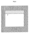
- Fig. 6 is a perspective view of the n-type single-crystalline silicon 11 according to the present embodiment viewed from the light-receiving surface-side.
- the light-receiving surface of the n-type single-crystalline silicon 11 is a (100) plane. As shown in Fig. 6 , a textured structure is formed on the light-receiving surface of the n-type single-crystalline silicon 11.
- the textured structure formed on the light-receiving surface of the n-type single-crystalline silicon 11 each has a height of several ⁇ m to several tens ⁇ m orderly in a direction vertical to the light-receiving surface.
- n-type single-crystalline silicon 11 a plurality of through holes is formed and each penetrates from the light-receiving surface to the back surface of the n-type single-crystalline silicon 11.
- Each of the through holes is formed in a substantially-quadrangular form in the planar view of the n-type single-crystalline silicon 11.
- the inner wall surface of the through hole is formed by four smooth surfaces B (in Fig.6 , only one smooth surface B is shown).
- a relief structure (not shown) is formed on each of the smooth surfaces B.
- the relief structure formed on the smooth surface B is smaller and gentler than that of the textured structure formed on the light-receiving surface.
- Such a relief structure has a height (zero point several ⁇ m to several ⁇ m) of about one-tenth of that of the textured structure of the light-receiving surface. Therefore, the inner wall surface of the through hole is formed to be smoother compared to the light-receiving surface.
- the arithmetic mean roughness (Ra) on the smooth surface B forming the inner wall surface of the through hole is smaller than the arithmetic mean roughness (Ra) of the light-receiving surface.
- a manufacturing method of a solar cell 1 according to the present embodiment will be described.
- a manufacturing method of a solar cell 1 according to the present embodiment includes a first etching process in which the inner wall surface of the through hole is etched, and a second etching process in which the light-receiving surface is etched.
- the first etching process the inner wall surface of the through hole is formed to be smoother compared to the light-receiving surface.
- the light-receiving surface is a (100) plane.
- four smooth surfaces that are (110) planes are exposed.
- Each of the smooth surfaces B is etched at an etching rate smaller than that of the light-receiving surface.
- the light-receiving surface is a (100) plane. Therefore, it is possible to prevent the relief structure from being formed on the inner wall surface of the through hole in the second etching process
- the smooth surface B having arithmetic mean roughness smaller than that of the light-receiving surface is formed.
- the insulating layer 17 can be formed to have uniform thickness. Accordingly, between the n-type single-crystalline silicon 11 and the through hole electrode 20 on the smooth surface B, occurrence of the short circuit can be suppressed. As a result, the output characteristics of the solar cell 1 can be improved.
- the third embodiment of the present invention will be described hereinbelow.
- the difference between the present embodiment and the forgoing first embodiment is that a semiconductor substrate mainly composed of polycrystal silicon is used in this embodiment.
- the schematic configurations of the solar cell module and the solar cell are the same as in the first embodiment. Accordingly, the difference from the forgoing first embodiment will mainly be described below.
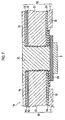
- Fig. 7 is an enlarged cross-sectional view of the solar cell 1a according to the present embodiment.
- the photoelectric conversion part 50 includes an n-type polycrystalline silicon substrate 51, a p-type polycrystal silicon layer 52, an anti-reflection film 53, and n-type polycrystal silicon layer 54.
- the n-type polycrystalline silicon substrate 51 is mainly composed of polycrystal silicon, and has a thickness of about 300 ⁇ m.
- the n-type polycrystalline silicon substrate 51 has through holes penetrating from the light-receiving surface to the back surface of the n-type polycrystalline silicon substrate 51.
- the through hole electrode 20 is provided inside the through hole.
- a fine textured structure is formed on the light-receiving surface of the n-type polycrystalline silicon substrate 51.
- the texture has a height of several ⁇ m to several tens ⁇ m.
- the p-type polycrystal silicon layer 52 is a semiconductor layer formed by a doping of p-type impurities on the light-receiving surface of the n-type polycrystalline silicon substrate 51.
- the p-type polycrystal silicon layer 52 forms a semiconductor p/n junction with the n-type polycrystalline silicon substrate 51.
- the anti-reflection film 53 is formed on the p-type polycrystal silicon layer 52.
- the anti-reflection film 53 can be formed by using SiN, SiO 2 and the like.
- the n-type polycrystal silicon layer 54 is a semiconductor layer formed by a doping of n-type impurities on the back surface of the n-type polycrystalline silicon substrate 51. Thereby, a so-called BSF structure is formed.
- the insulating layer 17 is provided on the inner wall surface of the through hole formed on the n-type polycrystalline silicon substrate 51, while extending from the inner wall surface to the back surface of the n-type polycrystal silicon layer 54.
- the insulating layer 17 insulates the n-type polycrystalline silicon substrate 51 from the through hole electrode 20.
- the insulating layer 17 can be formed of SiN.
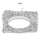
- Fig. 8 is a perspective view of the n-type polycrystalline silicon substrate 51 according to the present embodiment viewed from the light-receiving surface-side.
- the textured structure has a height of several ⁇ m to several tens ⁇ m in a direction vertical to the light-receiving surface.
- each of the through holes penetrating from the light-receiving surface to the back surface is formed.
- Each of the through holes is formed in a circle form in a plan view of the n-type polycrystalline silicon substrate 51.
- the inner wall surface of the through hole is configured by a uniformly smooth surface C.
- a relief structure (not shown) is formed on the uniformly smooth surface C.
- the relief structure formed on the uniformly smooth surface C is smaller and gentler than that of the textured structure formed on the light-receiving surface.
- Such a relief structure has a height (zero point several ⁇ m to several ⁇ m) of about one-tenth of that of the textured structure on the light-receiving surface.
- the inner wall surface of the through hole is formed to be smoother compared to the light-receiving surface.
- the arithmetic mean roughness (Ra) of the smooth surface C forming the inner wall surface of the through hole is smaller than arithmetic mean roughness (Ra) on the light-receiving surface.
- a manufacturing method of a solar cell 1a according to the present embodiment will be described.
- a manufacturing method of a solar cell 1 a includes a the first etching process in which the inner wall surface of the through hole is isotropically etched, and the second etching process in which the light-receiving surface is isotropically etched.
- the first etching process the inner wall surface of the through hole is formed to be smoother compared to the light-receiving surface.
- the first etching process uses a fluorinated nitrate solution prepared by mixing 69.5% nitric acid (HNO 3 ) and 49% hydrofluoric acid (HF) in a ratio of 10:1
- the second etching, process uses a fluorinated nitrate solution prepared by mixing 69.5% nitric acid (HNO 3 ) and 49% hydrofluoric acid (HF) in a ratio of 1:5 to 15.
- the etching processes can be respectively performed under different conditions, on the inner wall surface of the through hole and on the light-receiving surface. Therefore, suitable etching processes for both of the inner wall surface of the through hole and the light-receiving surface can be respectively performed.
- an etching rate is increased with relatively high concentration of the etching solution, so that an over-etched state is created.
- a gentle relief structure having a height of zero point several ⁇ m to several ⁇ m is formed on the inner wall surface of the through hole.
- a textured structure having a height of several ⁇ m to several tens ⁇ m suitable for a solar cell is formed.
- the through hole is covered with an anti-etching mask in the second etching process. Therefore, it is possible to prevent a relief structure from being formed on the inner wall surface of the through hole in the second etching process.
- the inner wall surface of the through hole is formed to be smoother compared to the light-receiving surface.
- the smooth surface C having arithmetic mean roughness smaller than that of the light-receiving surface is formed on the inner wall of the through hole, On such a smooth surface C, the insulating layer 17 can be formed to have uniform thickness. Accordingly, between the n-type polycrystalline silicon substrate 51 and the through hole electrode 20 on the smooth surface C, occurrence of the short circuit can be suppressed As a result, the output characteristics of the solar cell 1a can be improved.
- silicon substrates having an n-conductivity type (n-type single-crystalline silicon 11, n-type polycrystalline silicon substrate 51) are used, while a silicon substrate having a p-conductivity type may be used.
- etching solutions are used in the first and second etching processes
- different kinds of etching solutions may be used in each etching process.
- the present invention does not specify the etching solution used in the first and second etching process.
- the etching solution used in the first etching process only needs to have an etching performance higher than that of the etching solution used in the second etching process.
- isotropic etching is carried out in the first and second etching processes, while anisotropic etching may be carried out.
- an HIT type solar cell is given as an example to describe a solar cell, while the present invention can be applied to a general solar cell substrate in which p/n, p/i/n, i/n, or i/p semiconductor junction is formed.
- an n-type single-crystalline silicon substrate was prepared. Then, a plurality of through holes was formed in the n-type single-crystalline silicon substrate by using a YAG laser.
- an anisotropic etching process was performed on the surface of the n-type single-crystalline silicon substrate and the inner wall surface of each of the through holes, for 10 minutes using a high concentration NaOH water solution (about 5% by weight) at about 85°C.
- each of the through holes was covered with an anti-etching photoresist mask.
- an anisotropic etching process was performed on the surface of the n-type single-crystalline silicon substrate, for 30 minutes using a low concentration NaOH water solution (about 1.5% by weight) at about 85°C.
- an i-type amorphous silicon layer, an n-type amorphous silicon layer, and an ITO layer were formed on the back surface of the n-type single-crystalline silicon substrate by using a chemical vapor deposition (CVD) method.
- the i-type amorphous silicon layer, the p-type amorphous silicon layer, and the ITO layer were formed on the light-receiving surface of the n-type single-crystalline silicon substrate by using a chemical vapor deposition (CVD) method.
- a mask was provided at the circumference of the back-surface-side opening of each of the through holes to form an insulating layer in each of the through holes, by using SiO, SiN and the like by use of a CVD method.
- the insulating layer was formed on the back surface while extending along the arrangement direction.
- thermosetting conductive paste was formed in a predetermined pattern in the ITO layer on the light-receiving surface-side and the back-surface-side by using a screen printing method. Further, a thermosetting conductive paste was formed in a predetermined pattern on the back surface of the insulating layer.
- an n-type single-crystalline silicon substrate which was a (100) plane, was prepared. Then, a plurality of through holes was formed in the n-type single-crystalline silicon substrate by using a YAG laser. The through hole was formed in a roughly quadrangular form in its plan view to expose a (110) plane on the inner wall of the through hole.
- an anisotropic etching processing was performed on the surface of the n-type single-crystalline silicon substrate and the inner wall surface of each of the through holes, for 10 minutes by using a high concentration NaOH water solution (about 5% by weight) at about 85°C.
- an anisotropic etching processing was performed on the surface of the n-type single-crystalline silicon substrate, for 40 minutes by using a low concentration NaOH water solution (about 1.5% by weight) at about 85°C.
- the i-type amorphous silicon layer, the n-type amorphous silicon layer, and the ITO layer were formed on the back surface of the n-type single-crystalline silicon substrate by using a chemical vapor deposition (CVD) method.
- CVD chemical vapor deposition
- the i-type amorphous silicon layer, the p-type amorphous silicon layer, and the ITO layer were formed on the light-receiving surface of the n-type single-crystalline silicon substrate.
- a mask was provided at the circumference of the back-surface-side opening of each of the through holes to form an insulating layer in the through hole using SiO, SiN and the like by use of a CVD method.
- an insulating layer was formed on the back surface while extending along the arrangement direction.
- thermosetting conductive paste was formed in a predetermined pattern on the light-receiving surface-side and on the back-surface-side of the ITO layer, by using a screen printing method.
- a bus bar electrode was formed in a predetermined pattern on the back-surface-side of the insulating layer,
- the through holes were not formed previously in the n-type single-crystalline silicon substrate.
- the through holes were formed by using a YAG laser after the solar cell substrate was formed. An etching processing was not performed on the inner wall surface of each of the through holes. Other processes were the same as in the forgoing example 1.
- Example 2 With respect to Example 1, Example 2 and the prior example, the arithmetic mean roughness (Ra) on the light-receiving surface and the arithmetic mean roughness (Ra) on the inner wall surface of the through hole were measured.
- a laser microscope VK-970 available from Keyence Corporation was used to measure the arithmetic mean roughness (Ra) to calculate an average value in ten portions of each surface.
- the Ra was calculated by averaging the absolute values of the heights of irregularities over a reference length.
- Example 1 With respect to the Example 1, Example 2, and prior example, various characteristics of each solar cell were measured.
- Fig. 9 shows the relationship between the value of an inner wall surface Ra/a light-receiving surface Ra and the value of solar cell characteristics (F. F).
- the value of Inner Wall Surface (Ra)/Light-receiving surface (Ra) according to Examples 1 and 2 is smaller than the value of Inner Wall Surface (Ra)/Light-receiving surface (Ra) according to the Prior Example, and smaller than 1.00.
- the inner wall surface of the through hole is smoothened in Examples 1 and 2.
- the insulating layer is uniformly formed on the inner wall of the through hole. This uniformly formed insulating layer makes it possible to prevent an occurrence of a leak current between the through hole electrode and the substrate.
- the F. F value according to Examples 1 and 2 is larger than the F. F value according to Prior Example.
Landscapes
- Photovoltaic Devices (AREA)
- Weting (AREA)
Applications Claiming Priority (1)
| Application Number | Priority Date | Filing Date | Title |
|---|---|---|---|
| JP2007311586A JP2009135338A (ja) | 2007-11-30 | 2007-11-30 | 太陽電池及び太陽電池の製造方法 |
Publications (2)
| Publication Number | Publication Date |
|---|---|
| EP2065941A2 true EP2065941A2 (de) | 2009-06-03 |
| EP2065941A3 EP2065941A3 (de) | 2011-11-30 |
Family
ID=40474647
Family Applications (1)
| Application Number | Title | Priority Date | Filing Date |
|---|---|---|---|
| EP08253855A Withdrawn EP2065941A3 (de) | 2007-11-30 | 2008-12-01 | Solarzelle und Herstellungsverfahren dafür |
Country Status (4)
| Country | Link |
|---|---|
| US (1) | US20090139570A1 (de) |
| EP (1) | EP2065941A3 (de) |
| JP (1) | JP2009135338A (de) |
| CN (1) | CN101447516B (de) |
Cited By (1)
| Publication number | Priority date | Publication date | Assignee | Title |
|---|---|---|---|---|
| EP2863441A1 (de) * | 2013-10-21 | 2015-04-22 | Applied Materials Italia S.R.L. | Verfahren zur Herstellung eines Rückseitenkontakts in einer Solarzellenvorrichtung und Solarzellenvorrichtung |
Families Citing this family (34)
| Publication number | Priority date | Publication date | Assignee | Title |
|---|---|---|---|---|
| WO2011072161A2 (en) | 2009-12-09 | 2011-06-16 | Solexel, Inc. | High-efficiency photovoltaic back-contact solar cell structures and manufacturing methods using thin planar semiconductors |
| CN102132420A (zh) * | 2008-08-22 | 2011-07-20 | 三洋电机株式会社 | 太阳能电池模块、太阳能电池和太阳能电池模块的制造方法 |
| KR101573934B1 (ko) * | 2009-03-02 | 2015-12-11 | 엘지전자 주식회사 | 태양 전지 및 그 제조 방법 |
| KR101199822B1 (ko) * | 2009-04-27 | 2012-11-09 | 쿄세라 코포레이션 | 태양 전지 소자, 분할 태양 전지 소자, 태양 전지 모듈 및 전자기기 |
| JP2010283339A (ja) * | 2009-05-02 | 2010-12-16 | Semiconductor Energy Lab Co Ltd | 光電変換装置及びその作製方法 |
| KR20100135618A (ko) * | 2009-06-17 | 2010-12-27 | 삼성전자주식회사 | 태양 전지 및 그 제조 방법 |
| US20110041910A1 (en) * | 2009-08-18 | 2011-02-24 | Semiconductor Energy Laboratory Co., Ltd. | Photoelectric conversion device and manufacturing method thereof |
| KR20110024947A (ko) * | 2009-09-03 | 2011-03-09 | 삼성전자주식회사 | 태양 전지 |
| US20110068367A1 (en) * | 2009-09-23 | 2011-03-24 | Sierra Solar Power, Inc. | Double-sided heterojunction solar cell based on thin epitaxial silicon |
| US8115097B2 (en) | 2009-11-19 | 2012-02-14 | International Business Machines Corporation | Grid-line-free contact for a photovoltaic cell |
| CN102859712A (zh) * | 2010-04-20 | 2013-01-02 | 京瓷株式会社 | 太阳能电池元件及使用该太阳能电池元件的太阳能电池模块 |
| US9441295B2 (en) | 2010-05-14 | 2016-09-13 | Solarcity Corporation | Multi-channel gas-delivery system |
| US9240513B2 (en) | 2010-05-14 | 2016-01-19 | Solarcity Corporation | Dynamic support system for quartz process chamber |
| DE102010017180A1 (de) * | 2010-06-01 | 2011-12-01 | Solarworld Innovations Gmbh | Solarzelle, Solarmodul, und Verfahren zum Verdrahten einer Solarzelle, und Kontaktdraht |
| JP2011258767A (ja) * | 2010-06-09 | 2011-12-22 | Sharp Corp | 太陽電池 |
| KR101044606B1 (ko) * | 2010-07-29 | 2011-06-29 | 엘지전자 주식회사 | 태양전지 패널 |
| MY158500A (en) | 2010-08-05 | 2016-10-14 | Solexel Inc | Backplane reinforcement and interconnects for solar cells |
| DE102010048437B4 (de) * | 2010-10-15 | 2014-06-05 | Centrotherm Photovoltaics Ag | Solarzelle mit dielektrischer Rückseitenbeschichtung und Verfahren zu deren Herstellung |
| CN102610666A (zh) * | 2011-01-20 | 2012-07-25 | 无锡尚德太阳能电力有限公司 | 金属绕穿型背接触太阳电池、制备方法及其组件 |
| EP2757591B1 (de) * | 2011-09-13 | 2017-08-23 | Kyocera Corporation | Solarzellenmodul |
| US8894868B2 (en) * | 2011-10-06 | 2014-11-25 | Electro Scientific Industries, Inc. | Substrate containing aperture and methods of forming the same |
| JP6250552B2 (ja) * | 2011-12-30 | 2017-12-20 | ソレクセル、インコーポレイテッド | マルチレベルソーラーセルメタライゼーション |
| US9293624B2 (en) * | 2012-12-10 | 2016-03-22 | Sunpower Corporation | Methods for electroless plating of a solar cell metallization layer |
| MY175806A (en) * | 2013-03-15 | 2020-07-09 | Sunpower Corp | Conductivity enhancement of solar cells |
| CN103730522A (zh) * | 2014-01-28 | 2014-04-16 | 友达光电股份有限公司 | 光电转换结构、应用其的太阳能电池及其制造方法 |
| JP2017518626A (ja) | 2015-02-17 | 2017-07-06 | ソーラーシティ コーポレーション | 太陽電池の製造歩留まりを向上させる方法及びシステム |
| US20160359080A1 (en) | 2015-06-07 | 2016-12-08 | Solarcity Corporation | System, method and apparatus for chemical vapor deposition |
| US9748434B1 (en) | 2016-05-24 | 2017-08-29 | Tesla, Inc. | Systems, method and apparatus for curing conductive paste |
| US9954136B2 (en) | 2016-08-03 | 2018-04-24 | Tesla, Inc. | Cassette optimized for an inline annealing system |
| CN109564946B (zh) * | 2016-08-15 | 2023-10-03 | 夏普株式会社 | 光电转换元件以及光电转换装置 |
| US10115856B2 (en) | 2016-10-31 | 2018-10-30 | Tesla, Inc. | System and method for curing conductive paste using induction heating |
| EP3358630B1 (de) * | 2017-02-06 | 2020-04-15 | IMEC vzw | Teilweise durchscheinende photovoltaische module und verfahren zur herstellung |
| WO2019109671A1 (zh) * | 2017-12-05 | 2019-06-13 | 君泰创新(北京)科技有限公司 | 太阳能电池片及其制备方法、太阳能电池串以及光伏组件 |
| EP3671866A1 (de) * | 2018-12-18 | 2020-06-24 | Nederlandse Organisatie voor toegepast- natuurwetenschappelijk onderzoek TNO | Fotovoltaische vorrichtung und verfahren zur herstellung davon |
Citations (2)
| Publication number | Priority date | Publication date | Assignee | Title |
|---|---|---|---|---|
| JPS6482570A (en) | 1987-09-24 | 1989-03-28 | Mitsubishi Electric Corp | Manufacture of photoelectric conversion device |
| JP2007311586A (ja) | 2006-05-19 | 2007-11-29 | Nippon Steel Corp | 炭化珪素単結晶ウェハ表面の仕上げ研磨方法 |
Family Cites Families (7)
| Publication number | Priority date | Publication date | Assignee | Title |
|---|---|---|---|---|
| WO1989005521A1 (en) * | 1987-12-03 | 1989-06-15 | Spectrolab, Inc. | Solar cell panel |
| US5425816A (en) * | 1991-08-19 | 1995-06-20 | Spectrolab, Inc. | Electrical feedthrough structure and fabrication method |
| JP3619053B2 (ja) * | 1999-05-21 | 2005-02-09 | キヤノン株式会社 | 光電変換装置の製造方法 |
| JP4222992B2 (ja) * | 2004-09-29 | 2009-02-12 | 三洋電機株式会社 | 光起電力装置 |
| WO2006120735A1 (ja) * | 2005-05-11 | 2006-11-16 | Mitsubishi Denki Kabushiki Kaisha | 太陽電池およびその製造方法 |
| WO2007099955A1 (ja) * | 2006-03-01 | 2007-09-07 | Sanyo Electric Co., Ltd. | 太陽電池セル、及び、この太陽電池セルを用いた太陽電池モジュール |
| JP2007311425A (ja) * | 2006-05-16 | 2007-11-29 | Nippon Telegr & Teleph Corp <Ntt> | 太陽電池の製造方法および太陽電池 |
-
2007
- 2007-11-30 JP JP2007311586A patent/JP2009135338A/ja active Pending
-
2008
- 2008-12-01 US US12/325,313 patent/US20090139570A1/en not_active Abandoned
- 2008-12-01 CN CN2008101784881A patent/CN101447516B/zh not_active Expired - Fee Related
- 2008-12-01 EP EP08253855A patent/EP2065941A3/de not_active Withdrawn
Patent Citations (2)
| Publication number | Priority date | Publication date | Assignee | Title |
|---|---|---|---|---|
| JPS6482570A (en) | 1987-09-24 | 1989-03-28 | Mitsubishi Electric Corp | Manufacture of photoelectric conversion device |
| JP2007311586A (ja) | 2006-05-19 | 2007-11-29 | Nippon Steel Corp | 炭化珪素単結晶ウェハ表面の仕上げ研磨方法 |
Cited By (1)
| Publication number | Priority date | Publication date | Assignee | Title |
|---|---|---|---|---|
| EP2863441A1 (de) * | 2013-10-21 | 2015-04-22 | Applied Materials Italia S.R.L. | Verfahren zur Herstellung eines Rückseitenkontakts in einer Solarzellenvorrichtung und Solarzellenvorrichtung |
Also Published As
| Publication number | Publication date |
|---|---|
| CN101447516A (zh) | 2009-06-03 |
| CN101447516B (zh) | 2012-07-04 |
| JP2009135338A (ja) | 2009-06-18 |
| US20090139570A1 (en) | 2009-06-04 |
| EP2065941A3 (de) | 2011-11-30 |
Similar Documents
| Publication | Publication Date | Title |
|---|---|---|
| US20090139570A1 (en) | Solar cell and a manufacturing method of the solar cell | |
| EP4290588A1 (de) | Solarzelle und photovoltaisches modul | |
| EP2434548B1 (de) | Solarzelle und Verfahren zu ihrer Herstellung | |
| US7902454B2 (en) | Solar cell, solar cell module, and method of manufacturing the solar cell | |
| US8569100B2 (en) | Solar cell and manufacturing method thereof | |
| KR101661768B1 (ko) | 태양전지 및 이의 제조 방법 | |
| JP5025184B2 (ja) | 太陽電池素子及びこれを用いた太陽電池モジュール、並びに、これらの製造方法 | |
| EP2937910A1 (de) | Solarzelle und herstellungsverfahren dafür | |
| US20180122964A1 (en) | Solar battery and solar battery module | |
| CN101765920B (zh) | 太阳能电池模块 | |
| EP2212920B1 (de) | Solarzelle, verfahren zu ihrer herstellung und solarzellenmodul | |
| EP4539128A1 (de) | Solarzelle, verfahren zu ihrer herstellung und fotovoltaisches modul | |
| JP6785427B2 (ja) | 太陽電池素子および太陽電池モジュール | |
| JP2008270743A (ja) | 太陽電池モジュール | |
| EP2624306A1 (de) | Verfahren zur herstellung von solarzellen | |
| US9997647B2 (en) | Solar cells and manufacturing method thereof | |
| US20130160840A1 (en) | Solar cell | |
| WO2011132707A1 (ja) | 太陽電池素子およびそれを用いた太陽電池モジュール | |
| CN104810415A (zh) | 太阳能电池以及太阳能电池的制造方法 | |
| US8889981B2 (en) | Photoelectric device | |
| JP2005353851A (ja) | 太陽電池モジュール | |
| JP2011146678A (ja) | 太陽電池素子の製造方法 | |
| CN120417557A (zh) | 太阳能电池和太阳能电池的制备方法 | |
| JP6143520B2 (ja) | 結晶シリコン系太陽電池およびその製造方法 | |
| JP2005260158A (ja) | 太陽電池モジュール |
Legal Events
| Date | Code | Title | Description |
|---|---|---|---|
| PUAI | Public reference made under article 153(3) epc to a published international application that has entered the european phase |
Free format text: ORIGINAL CODE: 0009012 |
|
| AK | Designated contracting states |
Kind code of ref document: A2 Designated state(s): AT BE BG CH CY CZ DE DK EE ES FI FR GB GR HR HU IE IS IT LI LT LU LV MC MT NL NO PL PT RO SE SI SK TR |
|
| AX | Request for extension of the european patent |
Extension state: AL BA MK RS |
|
| PUAL | Search report despatched |
Free format text: ORIGINAL CODE: 0009013 |
|
| AK | Designated contracting states |
Kind code of ref document: A3 Designated state(s): AT BE BG CH CY CZ DE DK EE ES FI FR GB GR HR HU IE IS IT LI LT LU LV MC MT NL NO PL PT RO SE SI SK TR |
|
| AX | Request for extension of the european patent |
Extension state: AL BA MK RS |
|
| RIC1 | Information provided on ipc code assigned before grant |
Ipc: H01L 31/0236 20060101ALI20111026BHEP Ipc: H01L 31/0376 20060101ALI20111026BHEP Ipc: H01L 31/075 20060101ALI20111026BHEP Ipc: H01L 31/0224 20060101AFI20111026BHEP |
|
| 17P | Request for examination filed |
Effective date: 20120524 |
|
| AKX | Designation fees paid |
Designated state(s): DE ES FR IT |
|
| STAA | Information on the status of an ep patent application or granted ep patent |
Free format text: STATUS: THE APPLICATION IS DEEMED TO BE WITHDRAWN |
|
| 18D | Application deemed to be withdrawn |
Effective date: 20130702 |