EP2071388A1 - Élément de commande de la lumière - Google Patents
Élément de commande de la lumière Download PDFInfo
- Publication number
- EP2071388A1 EP2071388A1 EP07828740A EP07828740A EP2071388A1 EP 2071388 A1 EP2071388 A1 EP 2071388A1 EP 07828740 A EP07828740 A EP 07828740A EP 07828740 A EP07828740 A EP 07828740A EP 2071388 A1 EP2071388 A1 EP 2071388A1
- Authority
- EP
- European Patent Office
- Prior art keywords
- electrode
- control device
- light control
- thin plate
- optical waveguide
- Prior art date
- Legal status (The legal status is an assumption and is not a legal conclusion. Google has not performed a legal analysis and makes no representation as to the accuracy of the status listed.)
- Granted
Links
- 230000003287 optical effect Effects 0.000 claims abstract description 141
- 230000005684 electric field Effects 0.000 claims abstract description 38
- 230000005693 optoelectronics Effects 0.000 claims abstract description 12
- 239000000758 substrate Substances 0.000 claims description 54
- 238000000059 patterning Methods 0.000 claims description 7
- 239000010410 layer Substances 0.000 description 19
- 238000004088 simulation Methods 0.000 description 16
- 238000011156 evaluation Methods 0.000 description 11
- 230000000644 propagated effect Effects 0.000 description 11
- 238000010586 diagram Methods 0.000 description 10
- 239000000463 material Substances 0.000 description 9
- 238000000034 method Methods 0.000 description 9
- VYPSYNLAJGMNEJ-UHFFFAOYSA-N Silicium dioxide Chemical compound O=[Si]=O VYPSYNLAJGMNEJ-UHFFFAOYSA-N 0.000 description 7
- 239000000853 adhesive Substances 0.000 description 6
- 230000001070 adhesive effect Effects 0.000 description 6
- 239000013078 crystal Substances 0.000 description 6
- GQYHUHYESMUTHG-UHFFFAOYSA-N lithium niobate Chemical compound [Li+].[O-][Nb](=O)=O GQYHUHYESMUTHG-UHFFFAOYSA-N 0.000 description 5
- 238000004519 manufacturing process Methods 0.000 description 5
- 230000000694 effects Effects 0.000 description 4
- 239000012141 concentrate Substances 0.000 description 3
- 239000010931 gold Substances 0.000 description 3
- 229910052751 metal Inorganic materials 0.000 description 3
- 239000002184 metal Substances 0.000 description 3
- 230000010287 polarization Effects 0.000 description 3
- 239000000377 silicon dioxide Substances 0.000 description 3
- 206010012335 Dependence Diseases 0.000 description 2
- UMIVXZPTRXBADB-UHFFFAOYSA-N benzocyclobutene Chemical compound C1=CC=C2CCC2=C1 UMIVXZPTRXBADB-UHFFFAOYSA-N 0.000 description 2
- 229910052681 coesite Inorganic materials 0.000 description 2
- 229910052906 cristobalite Inorganic materials 0.000 description 2
- 230000003247 decreasing effect Effects 0.000 description 2
- 239000011521 glass Substances 0.000 description 2
- 229910052744 lithium Inorganic materials 0.000 description 2
- 229910052682 stishovite Inorganic materials 0.000 description 2
- 229920001187 thermosetting polymer Polymers 0.000 description 2
- 229910052905 tridymite Inorganic materials 0.000 description 2
- 239000004593 Epoxy Substances 0.000 description 1
- 229910003327 LiNbO3 Inorganic materials 0.000 description 1
- WHXSMMKQMYFTQS-UHFFFAOYSA-N Lithium Chemical compound [Li] WHXSMMKQMYFTQS-UHFFFAOYSA-N 0.000 description 1
- RTAQQCXQSZGOHL-UHFFFAOYSA-N Titanium Chemical compound [Ti] RTAQQCXQSZGOHL-UHFFFAOYSA-N 0.000 description 1
- 238000010521 absorption reaction Methods 0.000 description 1
- 239000012790 adhesive layer Substances 0.000 description 1
- PNEYBMLMFCGWSK-UHFFFAOYSA-N aluminium oxide Inorganic materials [O-2].[O-2].[O-2].[Al+3].[Al+3] PNEYBMLMFCGWSK-UHFFFAOYSA-N 0.000 description 1
- 230000015572 biosynthetic process Effects 0.000 description 1
- 238000000576 coating method Methods 0.000 description 1
- 238000004891 communication Methods 0.000 description 1
- 150000001875 compounds Chemical class 0.000 description 1
- 238000013461 design Methods 0.000 description 1
- 238000009792 diffusion process Methods 0.000 description 1
- 238000006073 displacement reaction Methods 0.000 description 1
- 238000001312 dry etching Methods 0.000 description 1
- PCHJSUWPFVWCPO-UHFFFAOYSA-N gold Chemical compound [Au] PCHJSUWPFVWCPO-UHFFFAOYSA-N 0.000 description 1
- 229910052737 gold Inorganic materials 0.000 description 1
- 229910052738 indium Inorganic materials 0.000 description 1
- 229910052746 lanthanum Inorganic materials 0.000 description 1
- FZLIPJUXYLNCLC-UHFFFAOYSA-N lanthanum atom Chemical compound [La] FZLIPJUXYLNCLC-UHFFFAOYSA-N 0.000 description 1
- 238000005259 measurement Methods 0.000 description 1
- 239000000203 mixture Substances 0.000 description 1
- 238000000206 photolithography Methods 0.000 description 1
- 239000010453 quartz Substances 0.000 description 1
- 239000011347 resin Substances 0.000 description 1
- 229920005989 resin Polymers 0.000 description 1
- 229910000679 solder Inorganic materials 0.000 description 1
- 230000002269 spontaneous effect Effects 0.000 description 1
- 230000008646 thermal stress Effects 0.000 description 1
- 238000001039 wet etching Methods 0.000 description 1
Images






Classifications
-
- G—PHYSICS
- G02—OPTICS
- G02F—OPTICAL DEVICES OR ARRANGEMENTS FOR THE CONTROL OF LIGHT BY MODIFICATION OF THE OPTICAL PROPERTIES OF THE MEDIA OF THE ELEMENTS INVOLVED THEREIN; NON-LINEAR OPTICS; FREQUENCY-CHANGING OF LIGHT; OPTICAL LOGIC ELEMENTS; OPTICAL ANALOGUE/DIGITAL CONVERTERS
- G02F1/00—Devices or arrangements for the control of the intensity, colour, phase, polarisation or direction of light arriving from an independent light source, e.g. switching, gating or modulating; Non-linear optics
- G02F1/01—Devices or arrangements for the control of the intensity, colour, phase, polarisation or direction of light arriving from an independent light source, e.g. switching, gating or modulating; Non-linear optics for the control of the intensity, phase, polarisation or colour
- G02F1/03—Devices or arrangements for the control of the intensity, colour, phase, polarisation or direction of light arriving from an independent light source, e.g. switching, gating or modulating; Non-linear optics for the control of the intensity, phase, polarisation or colour based on ceramics or electro-optical crystals, e.g. exhibiting Pockels effect or Kerr effect
- G02F1/035—Devices or arrangements for the control of the intensity, colour, phase, polarisation or direction of light arriving from an independent light source, e.g. switching, gating or modulating; Non-linear optics for the control of the intensity, phase, polarisation or colour based on ceramics or electro-optical crystals, e.g. exhibiting Pockels effect or Kerr effect in an optical waveguide structure
- G02F1/0356—Devices or arrangements for the control of the intensity, colour, phase, polarisation or direction of light arriving from an independent light source, e.g. switching, gating or modulating; Non-linear optics for the control of the intensity, phase, polarisation or colour based on ceramics or electro-optical crystals, e.g. exhibiting Pockels effect or Kerr effect in an optical waveguide structure controlled by a high-frequency electromagnetic wave component in an electric waveguide structure
-
- G—PHYSICS
- G02—OPTICS
- G02F—OPTICAL DEVICES OR ARRANGEMENTS FOR THE CONTROL OF LIGHT BY MODIFICATION OF THE OPTICAL PROPERTIES OF THE MEDIA OF THE ELEMENTS INVOLVED THEREIN; NON-LINEAR OPTICS; FREQUENCY-CHANGING OF LIGHT; OPTICAL LOGIC ELEMENTS; OPTICAL ANALOGUE/DIGITAL CONVERTERS
- G02F1/00—Devices or arrangements for the control of the intensity, colour, phase, polarisation or direction of light arriving from an independent light source, e.g. switching, gating or modulating; Non-linear optics
- G02F1/01—Devices or arrangements for the control of the intensity, colour, phase, polarisation or direction of light arriving from an independent light source, e.g. switching, gating or modulating; Non-linear optics for the control of the intensity, phase, polarisation or colour
- G02F1/03—Devices or arrangements for the control of the intensity, colour, phase, polarisation or direction of light arriving from an independent light source, e.g. switching, gating or modulating; Non-linear optics for the control of the intensity, phase, polarisation or colour based on ceramics or electro-optical crystals, e.g. exhibiting Pockels effect or Kerr effect
- G02F1/0305—Constructional arrangements
- G02F1/0316—Electrodes
-
- G—PHYSICS
- G02—OPTICS
- G02F—OPTICAL DEVICES OR ARRANGEMENTS FOR THE CONTROL OF LIGHT BY MODIFICATION OF THE OPTICAL PROPERTIES OF THE MEDIA OF THE ELEMENTS INVOLVED THEREIN; NON-LINEAR OPTICS; FREQUENCY-CHANGING OF LIGHT; OPTICAL LOGIC ELEMENTS; OPTICAL ANALOGUE/DIGITAL CONVERTERS
- G02F1/00—Devices or arrangements for the control of the intensity, colour, phase, polarisation or direction of light arriving from an independent light source, e.g. switching, gating or modulating; Non-linear optics
- G02F1/01—Devices or arrangements for the control of the intensity, colour, phase, polarisation or direction of light arriving from an independent light source, e.g. switching, gating or modulating; Non-linear optics for the control of the intensity, phase, polarisation or colour
- G02F1/21—Devices or arrangements for the control of the intensity, colour, phase, polarisation or direction of light arriving from an independent light source, e.g. switching, gating or modulating; Non-linear optics for the control of the intensity, phase, polarisation or colour by interference
- G02F1/225—Devices or arrangements for the control of the intensity, colour, phase, polarisation or direction of light arriving from an independent light source, e.g. switching, gating or modulating; Non-linear optics for the control of the intensity, phase, polarisation or colour by interference in an optical waveguide structure
- G02F1/2255—Devices or arrangements for the control of the intensity, colour, phase, polarisation or direction of light arriving from an independent light source, e.g. switching, gating or modulating; Non-linear optics for the control of the intensity, phase, polarisation or colour by interference in an optical waveguide structure controlled by a high-frequency electromagnetic component in an electric waveguide structure
-
- G—PHYSICS
- G02—OPTICS
- G02F—OPTICAL DEVICES OR ARRANGEMENTS FOR THE CONTROL OF LIGHT BY MODIFICATION OF THE OPTICAL PROPERTIES OF THE MEDIA OF THE ELEMENTS INVOLVED THEREIN; NON-LINEAR OPTICS; FREQUENCY-CHANGING OF LIGHT; OPTICAL LOGIC ELEMENTS; OPTICAL ANALOGUE/DIGITAL CONVERTERS
- G02F1/00—Devices or arrangements for the control of the intensity, colour, phase, polarisation or direction of light arriving from an independent light source, e.g. switching, gating or modulating; Non-linear optics
- G02F1/01—Devices or arrangements for the control of the intensity, colour, phase, polarisation or direction of light arriving from an independent light source, e.g. switching, gating or modulating; Non-linear optics for the control of the intensity, phase, polarisation or colour
- G02F1/21—Devices or arrangements for the control of the intensity, colour, phase, polarisation or direction of light arriving from an independent light source, e.g. switching, gating or modulating; Non-linear optics for the control of the intensity, phase, polarisation or colour by interference
- G02F1/212—Mach-Zehnder type
-
- G—PHYSICS
- G02—OPTICS
- G02F—OPTICAL DEVICES OR ARRANGEMENTS FOR THE CONTROL OF LIGHT BY MODIFICATION OF THE OPTICAL PROPERTIES OF THE MEDIA OF THE ELEMENTS INVOLVED THEREIN; NON-LINEAR OPTICS; FREQUENCY-CHANGING OF LIGHT; OPTICAL LOGIC ELEMENTS; OPTICAL ANALOGUE/DIGITAL CONVERTERS
- G02F2201/00—Constructional arrangements not provided for in groups G02F1/00 - G02F7/00
- G02F2201/12—Constructional arrangements not provided for in groups G02F1/00 - G02F7/00 electrode
- G02F2201/127—Constructional arrangements not provided for in groups G02F1/00 - G02F7/00 electrode travelling wave
Definitions
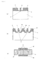
- a microwave signal is applied to the controlling electrode in order to control to modulate an optical wave propagated in the optical waveguide. Therefore, there is a need for achieving an impedance matching between a signal path, such as a coaxial cable which introduces microwaves into the optical modulator, and the controlling electrode in the optical modulator such that the microwave is efficiently propagated in the controlling electrode. For this reason, as shown in Fig. 1(a) , a shape of controlling electrode where a strip-shaped signal electrode 4 is interposed between grounding electrodes 5, that is, a coplanar type controlling electrode has been used.
- Patent Document 1 discloses a configuration that the optical waveguide is formed of a ridge type waveguide 20 and the grounding electrodes 5, 51, and 52 are disposed closer to the signal electrodes 4 and 41 in order to enhance an optical confinement of the optical waveguide and to more efficiently apply an electric field generated by the controlling electrode to the optical waveguide.
- this configuration it is possible to realize a reduction in driving voltage to some degree but it is essential to reduce the driving voltage further more in order to realize a high-speed modulation in a highfrequency band.
- Patent Document 2 discloses that the substrate is interposed between the controlling electrodes, and the electric field is applied in a direction (corresponding to a vertical direction in the case of the Z-axis cut substrate shown in Fig. 1(c) ) of high efficiency in the electro-optical effect.
- the optical modulator shown in Fig. 1(c) polarizes reversely the substrate having the electro-optical effect, and forms substrate regions 10 and 11 which are different from each other in a direction (a direction of arrow in Fig. 1(c) ) of a spontaneous polarization, and the optical waveguide 2 is formed in each substrate region.
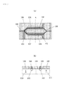
- Patent Document 3 discloses a configuration that the signal electrode which configures the controlling electrode is branched into two or more in the middle of the path, and applies the same signal electric field to plural optical waveguides.
- the signal paths are necessary to be set to have different impedances, for example, 50 ⁇ for the signal path of the signal electrode 103, and 100 ⁇ for the branched signal path of the branched signal electrodes 104 and 105 even though the signal paths are in the same light control device.
- the branched signal path is required to be adjusted to have a very high impedance of 70 ⁇ or more. For this reason, it is very difficult to obtain the reduction in driving voltage or the velocity matching between the microwave and the optical wave while adjusting such impedances.
- An advantage of some aspects of the present invention is to solve the above-mentioned problems and to provide a light control device, which is possible to realize a velocity matching between a microwave and an optical wave or an impedance matching of the microwaves even though a signal path having a high impedance of 70 ⁇ or more is required, and is possible to reduce a driving voltage.
- another advantage of some aspects of the present invention is to provide the light control device which can operate stably and suppress a rise in temperature of the light control device thanks to the reduction in driving voltage, and further to provide the light control device which can use a low-driving-voltage driving device which is inexpensive.
- planar type electrode of the present invention means a strip-shaped signal electrode interposed between grounding electrodes.
- the signal electrodes are formed as plural strip lines, and the plural strip lines are interposed between the grounding electrodes, or further the grounding electrodes are additionally disposed between the plural strip lines in the "coplanar type electrode.”
- the optical waveguide is a ridge type optical waveguide.
- the signal electrode or the grounding electrode includes a transparent electrode or an electrode in which a transparent electrode is disposed on the side of thin plate.
- a signal line for feeding the signal electrode is disposed so as to pass through a position above or below the grounding electrode of the first electrode, and a low-permittivity film is disposed between the signal line and the grounding electrode.
- the second electrode is a patterning electrode which has a shape corresponding to that of the optical waveguide.
- the grounding electrode of the first electrode is electrically connected with the grounding electrode of the second electrode via a through hole provided in the thin plate.
- the thin plate is bonded to a support substrate via an adhesion layer so as to interpose the first electrode or the second electrode.
- an impedance of the branched signal path is 70 ⁇ or more.
- At least a width W, a height T EL of the signal electrode of the branched signal path, a gap G between the signal electrode and the grounding electrode, and a depth D of a ridge when the optical waveguide is a ridge type optical waveguide are set such that a half-wavelength voltage Vpai in the branched signal path is 12 V ⁇ cm or less, an impedance Z is 70 ⁇ or more and 130 ⁇ or less, and a product of a reflection difference ⁇ n between a light and a microwave and a length L of an operation portion where an electric field of the branched signal path operates to the optical waveguide is 1.3 cm or less.
- a light control device having an electro-optical effect comprises a thin plate having a thickness of 10 ⁇ m or less, an optical waveguide formed in the thin plate, and a controlling electrode for controlling light which passes through the optical waveguide, wherein the controlling electrode includes a first electrode and a second electrode which are disposed so as to interpose the thin plate, wherein the first electrode has a coplanar type electrode structure which includes at least a signal electrode and a grounding electrode, wherein the second electrode includes at least a grounding electrode and is configured so as to apply an electric field to the optical waveguide in corporation with the signal electrode of the first electrode, and wherein the signal electrode of the first electrode includes a branched signal path in which at least one signal path is branched into two or more in the middle of the path.
- the light control device having a branched signal path of high impedance a velocity matching between a microwave and an optical wave or an impedance matching of the microwaves can be realized, and it is possible to provide the light control device capable of operating in high speed. Moreover, since a driving voltage can be reduced, it is possible to drive the light control device in high speed using an existing low-cost driving device, and thus the cost for the driving device can be reduced.
- the thin plate is polarized reversely, at least a part of an operation region in the thin plate where an electric field by the branched signal path operates can give rise to different optical modulations on the optical waveguide formed in the thin plate when an electric field is applied in the same direction, and a differential driving of the light control device can be easily realized by a simple controlling electrode or a driving circuit, and thus it is also possible to reduce a driving voltage.
- recesses which are disposed on the both sides of at least the ridge type waveguide are filled with a low-permittivity film. Therefore, it is possible to adjust a microwave refraction index or impedance of the controlling electrode, and thus a further proper refraction index or impedance of the microwave can be obtained.
- the second electrode is a patterning electrode which has a shape corresponding to that of the optical waveguide. Therefore, the electric field applied to the optical waveguide can be further concentrated, and the driving voltage can be further lowered.
- the grounding electrode of the first electrode is electrically connected with the grounding electrode of the second electrode via a through hole provided in the thin plate. Therefore, it is possible to apply the proper electric field described above to the optical waveguide, and an electric wiring for the light control device can be simplified.
- the thin plate is bonded to a support substrate via an adhesion layer so as to interpose the first electrode or the second electrode. Therefore, a mechanical strength of the thin plate can be reinforced, and thus it is possible to provide the light control device with high reliability.
- the light control device further comprises a support substrate which reinforces the thin plate, the first electrode or the second electrode is disposed on the support substrate. Therefore, flexibility in arrangement of the controlling electrode increases, and it is also possible to achieve a complex wiring such as an optical integrated circuit. Moreover, the number of the controlling electrodes disposed on the thin plate can be reduced, and thus it can reduce a risk of damage on the thin plate due to a thermal stress or the like on the thin plate.
- an impedance of the branched signal path is 70 ⁇ or more. Therefore, with respect to the light control device having a signal path of high impendance, the velocity matching between the microwave and the optical wave or the impedance matching of the microwaves can be realized, and it is possible to provide the light control device capable of operating in high speed. Moreover, since the driving voltage can be reduced, it is possible to drive the light control device in high speed using an existing low-cost driving device, and thus the cost for the driving device can be reduced.
- At least a width W, a height T EL of the signal electrode of the branched signal path, a gap G between the signal electrode and the grounding electrode, and a depth D of a ridge when the optical waveguide is a ridge type optical waveguide are set such that a half-wavelength voltage Vpai in the branched signal path is 12 V ⁇ cm or less, an impedance Z is 70 ⁇ or more and 130 ⁇ or less, and a product of a reflection difference ⁇ n between a light and a microwave and a length L of an operation portion where an electric field of the branched signal path operates to the optical waveguide is 1.3 cm or less.
- the light control device having a high impedance signal path it is possible to every easily realize the velocity matching between the microwave and the optical wave or the impedance matching of the microwaves only by adjusting a width or a height of the signal electrode or a gap between the signal electrode and the grounding electrode or a depth of the ridge or the like, and it is possible to provide the light control device capable of operating in high speed. Moreover, since the driving voltage can be reduced, it is possible to drive the light control device in high speed using an existing low-cost driving device, and thus the cost for the driving device can be reduced.
- a basic configuration of a light control device is characterized by a light control device having an electro-optical effect, comprising a thin plate having a thickness of 10 ⁇ m or less, an optical waveguide formed in the thin plate, and a controlling electrode for controlling light which passes through the optical waveguide, wherein the controlling electrode includes a first electrode and a second electrode which are disposed so as to interpose the thin plate, wherein the first electrode has a coplanar type electrode structure which includes at least a signal electrode and a grounding electrode, wherein the second electrode includes at least a grounding electrode and is configured so as to apply an electric field to the optical waveguide in corporation with the signal electrode of the first electrode, and wherein the signal electrode of the first electrode includes a branched signal path in which at least one signal path is branched into two or more in the middle of the path.
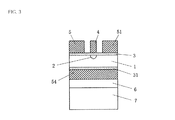
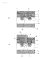
- Fig. 3 is a cross-sectional view illustrating a light control device according to an embodiment of the present invention and, particularly, illustrating a part extracted from a branched signal path in which at least one signal path is branched into two or more in the middle of the path as shown in Fig. 2 .
- Fig. 3 shows a case in which a Z-axis cut substrate (thin plate) 1 is used.
- a light control device in which an X-axis cut substrate is used includes a high impedance path such as the branched signal path, it is matter of course that the technique of the present invention is equally applicable.
- a thickness of the thin plate of the light control device of the present invention is preferably 10 ⁇ m or less.
- a substrate of the light control device is a thin plate, as in the case of Fig. 3 , it is possible to operate the light control device even though the first electrode and the second electrode are conversely disposed with respect to the thin plate 1.
- lithium niobate lithium tantalite, PLZT (lead lanthanum zirconate titanate), silica-based materials, and a composition thereof are available.
- lithium niobate (LN) or lithium tantalize (LT) crystal with high electro-optical effect is preferably used.
- a method of forming the electrode pattern through a photolithography technique and then using a liftoff technique, or a method of forming the electrode pattern in which a mask member is formed such that a predetermined electrode pattern is left and then subjected to a dry etching or a wet etching is available.
- the above-mentioned optical waveguide is formed on the substrate having a thickness of several hundreds ⁇ m, and a rear surface of the substrate is rubbed, so that the thin plate having a thickness of 10 ⁇ m or less is generated.
- the controlling electrode is formed in the surface of the thin plate.
- a process likely to undergo these thermal or mechanical impacts is performed before the substrate is rubbed to be thin.
- Material for the support substrate 7 can be used with various ones.
- low-permittivity materials such as quartz, glass, and alumina, or materials having a crystal orientation different from the thin plate.
- materials having the linear expansion coefficient equivalent to that of the thin plate be selected.
- adhesion layer 6 it is possible to use various adhesive materials, such as epoxy-based adhesive, thermosetting adhesive, ultraviolet curable adhesive, solder glass, and a thermosetting, a light curable or a light-induced viscosity resin adhesive sheet, to bond the thin plate 1 to the support substrate 7.
- adhesive materials such as epoxy-based adhesive, thermosetting adhesive, ultraviolet curable adhesive, solder glass, and a thermosetting, a light curable or a light-induced viscosity resin adhesive sheet, to bond the thin plate 1 to the support substrate 7.
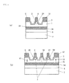
- Fig. 4 shows an application of the light control device of the present invention, which is an example where the optical waveguide is formed by the ridge type waveguide.
- the optical waveguide is formed by the ridge type waveguide.
- Fig. 4(a) shows the light control device where the optical waveguide shown in Fig. 3 is formed as a ridge type waveguide 20, where the optical wave propagated in the ridge portion 20 is confined. Since the electric field generated by the signal electrode 4 and the grounding electrode 5 (51) and the electric field generated by the signal electrode 4 and the grounding electrode 54 are intensively applied to the ridge portion 20, it contributes to a decrease in driving voltage of the light control device.
- Fig. 4(b) is a cross-sectional view illustrating the light control device including two branched signal paths as shown in Fig. 2(b) , which is adopted with the structure of Fig. 4(a) according to the present invention.
- Fig. 4(b) shows that two optical waveguides 2 are formed as the ridge type waveguide 20 and, a ridge portion corresponding to the grounding electrode 51 is formed between two optical waveguides.
- the signal electrodes 4 and 41 are disposed at locations corresponding to the ridge type waveguides 20, and the same signal is applied to the signal electrodes.
- Fig. 5 shows an application of the light control device of the present invention, which is an example where recesses forming the ridge type waveguide and a low-permittivity film is disposed between the signal electrode 4 and the grounding electrode 5 (51) to be a first electrode.
- the low-permittivity film With this arrangement of the low-permittivity film, the refraction index or the impedance of a microwave can be adjusted in the controlling electrode, and flexibility in wiring of the controlling electrode can be increased.
- materials of the low-permittivity film benzocyclobutene (BCB) or the like can be used, and as a method of manufacturing the low-permittivity film, a coating method can be used.
- BCB benzocyclobutene
- the low-permittivity film 8 can be formed so as to coat recesses formed on both sides of the ridge type waveguide 20, portions between the signal electrode 4 and the grounding electrode 5 (51), or the first electrode.
- a power feeding portion 43 of the signal electrode 4 is disposed to pass through a position above the grounding electrode 5, and the low-permittivity film 8 is disposed between the grounding electrode 4 and the power feeding portion 43. Therefore, the controlling electrode can be wired in three dimensions, and thus the flexibility in wiring design related to the controlling electrode can be increased.
- the grounding electrode is formed to pass through a position above the signal electrode (location away from the thin plate).
- Fig. 6 shows an application of the light control device of the present invention, which is an example where the optical waveguide 2 (ridge type waveguide 20) is formed on the rear surface (lower portion of the drawing) of the thin plate 1.
- the optical waveguide 2 is formed on the rear surface of the thin plate 1
- the signal electrode 4 and the grounding electrode 5 (51) which are the first electrode are formed on the surface of the thin plate.
- the grounding electrode 54 which is the second electrode is formed on the rear surface of the thin plate 1.
- the ridge portion 20 is possible to be applied with the electric field, especially, generated by the signal electrode 4 and the grounding electrode 54.
- the low-permittivity films 81 are formed at the recesses which form the ridge portion 20, if necessary.
- Fig. 7 shows an application of the light control device of the present invention, which is an example where transparent electrodes (9 and 91 to 94) are used to the electrode.
- transparent electrodes (9 and 91 to 94) are used to the electrode.
- Fig. 7(c) shows an example where the transparent electrode is used in a part (a side coming into contact with the thin plate 1) of the controlling electrode.
- the transparent electrode since the transparent electrode has high electrical resistivity in comparison with the metal electrode such as Au, it is possible to dispose the metal electrodes 140, 150, 151, and 152 by coming into contract with the transparent electrodes 9 or 93 to 94 for the purpose of reducing an electric resistance of an electrode.
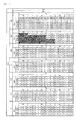
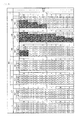
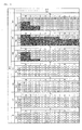
- the height T EL of the electrode was set to be 0.5, 1.0, 1.5, 2.0, 2.5, and 3.0 ( ⁇ m).
- the gap G between the electrodes was set by using a value normalized with the thickness t of the substrate so that G/t (denoted by "Gap/t” in the following drawing) was set to be 1.0, 2.25, 3.5, 4.75, and 6.0.
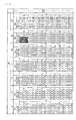
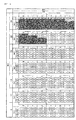
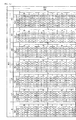
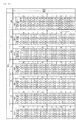
- portions which are satisfied with all the evaluation conditions (1) to (3) are illustrated as shade portions. It is understood from Figs. 11 to 22 illustrating the results according to the light control device of the invention that the light control device which satisfies the conditions of the above-mentioned high impedance path can be easily implemented by adjusting the width W of the signal electrode, the gap G between the signal electrode and the grounding electrode, the height T EL of the signal electrode or the grounding electrode, the depth D of the ridge of the ridge type optical waveguide, and the thickness t of the substrate.
- the thickness t of the substrate is any one of 2, 4, or 10 ⁇ m, a portion that satisfies the evaluation conditions is located in a range of W/t ⁇ 2.
- the upper limit value of the width W is specified such that the impedance Z drifts away from the evaluation conditions.
- the lower limit value of the width W is likely to be specified such that the half-wavelength voltage Vpai drifts away from the evaluation conditions.
- the width W becomes the better the result may be. In this case, it is specified by the limit of the electrode manufacture.
- the lower limit value of the gap G is specified when the impedance Z or the microwave refraction index NM drifts away from the evaluation conditions.
- the upper limit value of the gap G cannot be determined from a set range of the data, since the electric field weakens when the gap between the electrodes increases, the possibility that the upper limit of the gap G is limited by an increase of the half-wavelength voltage Vpai is high.
- the upper limit value of the height T EL is specified when the microwave refraction index NM drifts away from the evaluation conditions in the vicinity of the lower limit boundary of the width W and the impedance Z drifts away from the evaluation conditions in the vicinity of the upper limit boundary of the width W.
- the lower limit value of the height T EL cannot be determined from a set range of the data, since the electric resistance increases when the electrode becomes excessively thinner, the possibility that the lower limit value of the height T EL is limited by an increase of the half-wavelength voltage Vpai is high.
- the light control device of the present invention when the signal path having a high impedance of 70 ⁇ or more is required, the velocity matching between the microwave and the optical wave or the impedance matching of the microwaves can be realized. Moreover, it is possible to provide the light control device in which the driving voltage can be reduced. In addiction, thanks to the reduction in driving voltage, it is possible to suppress a rise in temperature of the light control device, and it is possible to provide the light control device which can operate stably. Further, it is possible to provide the light control device which can use a low-driving-voltage driving device which is inexpensive.
Landscapes
- Physics & Mathematics (AREA)
- Nonlinear Science (AREA)
- General Physics & Mathematics (AREA)
- Optics & Photonics (AREA)
- Electromagnetism (AREA)
- Chemical & Material Sciences (AREA)
- Engineering & Computer Science (AREA)
- Ceramic Engineering (AREA)
- Crystallography & Structural Chemistry (AREA)
- Optical Modulation, Optical Deflection, Nonlinear Optics, Optical Demodulation, Optical Logic Elements (AREA)
Applications Claiming Priority (2)
| Application Number | Priority Date | Filing Date | Title |
|---|---|---|---|
| JP2006270181A JP4110182B2 (ja) | 2006-09-30 | 2006-09-30 | 光制御素子 |
| PCT/JP2007/068999 WO2008038778A1 (fr) | 2006-09-30 | 2007-09-28 | Élément de commande de la lumière |
Publications (3)
| Publication Number | Publication Date |
|---|---|
| EP2071388A1 true EP2071388A1 (fr) | 2009-06-17 |
| EP2071388A4 EP2071388A4 (fr) | 2013-05-29 |
| EP2071388B1 EP2071388B1 (fr) | 2018-03-28 |
Family
ID=39230210
Family Applications (1)
| Application Number | Title | Priority Date | Filing Date |
|---|---|---|---|
| EP07828740.6A Not-in-force EP2071388B1 (fr) | 2006-09-30 | 2007-09-28 | Élément de commande de la lumière |
Country Status (5)
| Country | Link |
|---|---|
| US (1) | US7873244B2 (fr) |
| EP (1) | EP2071388B1 (fr) |
| JP (1) | JP4110182B2 (fr) |
| CN (1) | CN101512416B (fr) |
| WO (1) | WO2008038778A1 (fr) |
Cited By (1)
| Publication number | Priority date | Publication date | Assignee | Title |
|---|---|---|---|---|
| EP2141532A4 (fr) * | 2007-03-30 | 2013-03-06 | Sumitomo Osaka Cement Co Ltd | Élément de commande de lumière |
Families Citing this family (28)
| Publication number | Priority date | Publication date | Assignee | Title |
|---|---|---|---|---|
| JP5598221B2 (ja) | 2010-09-30 | 2014-10-01 | 住友大阪セメント株式会社 | 光制御素子 |
| JP2012078473A (ja) * | 2010-09-30 | 2012-04-19 | Sumitomo Osaka Cement Co Ltd | 光導波路素子 |
| JP5773440B2 (ja) | 2012-01-31 | 2015-09-02 | 住友大阪セメント株式会社 | 光変調器 |
| JP2013246320A (ja) * | 2012-05-25 | 2013-12-09 | Japan Oclaro Inc | 半導体光素子、及び光モジュール |
| TW201426151A (zh) * | 2012-12-19 | 2014-07-01 | Hon Hai Prec Ind Co Ltd | 電光調製器 |
| JP5711287B2 (ja) * | 2013-03-26 | 2015-04-30 | 住友大阪セメント株式会社 | 光制御デバイス |
| CN104155779A (zh) * | 2013-05-14 | 2014-11-19 | 鸿富锦精密工业(深圳)有限公司 | 电光调变器 |
| US9244296B2 (en) * | 2013-11-15 | 2016-01-26 | Tdk Corporation | Optical modulator |
| JP2015172629A (ja) * | 2014-03-11 | 2015-10-01 | 富士通オプティカルコンポーネンツ株式会社 | 光変調器 |
| GB201611576D0 (en) * | 2016-07-01 | 2016-08-17 | Oclaro Tech Ltd | Ground structure in RF waveguide array |
| WO2018014302A1 (fr) | 2016-07-21 | 2018-01-25 | 华为技术有限公司 | Modulateur électro-optique |
| US10295849B2 (en) * | 2016-12-16 | 2019-05-21 | Lumentum Operations Llc | Optical modulator |
| JP7115483B2 (ja) * | 2017-08-24 | 2022-08-09 | Tdk株式会社 | 光変調器 |
| JP7073963B2 (ja) * | 2018-07-24 | 2022-05-24 | 住友大阪セメント株式会社 | 光導波路素子 |
| CN109031708A (zh) * | 2018-09-29 | 2018-12-18 | 深圳市芯思杰智慧传感技术有限公司 | 一种具有预相位调制功能的光波导相位调制器芯片 |
| JP7118844B2 (ja) * | 2018-10-03 | 2022-08-16 | 株式会社日本製鋼所 | 光変調器、光変調器用基板、光変調器の製造方法及び光変調器用基板の製造方法 |
| JP7419806B2 (ja) * | 2019-12-26 | 2024-01-23 | 住友大阪セメント株式会社 | 光導波路素子および光変調器 |
| JP7463722B2 (ja) * | 2019-12-26 | 2024-04-09 | 住友大阪セメント株式会社 | 光導波路素子および光変調器 |
| WO2021161747A1 (fr) * | 2020-02-14 | 2021-08-19 | Tdk株式会社 | Élément guide d'ondes optique et élément de modulation de lumière |
| JP7526584B2 (ja) | 2020-04-21 | 2024-08-01 | 富士通オプティカルコンポーネンツ株式会社 | 光導波路デバイス |
| JP7526583B2 (ja) | 2020-04-21 | 2024-08-01 | 富士通オプティカルコンポーネンツ株式会社 | 光導波路デバイスおよび光導波路デバイスの製造方法 |
| CN113655564A (zh) * | 2020-05-12 | 2021-11-16 | 天津领芯科技发展有限公司 | 一种铌酸锂薄膜光波导结构、芯片及其制备方法 |
| JP7547779B2 (ja) * | 2020-05-15 | 2024-09-10 | 富士通オプティカルコンポーネンツ株式会社 | 光デバイス、及びこれを用いた光送受信機 |
| JP2022013232A (ja) * | 2020-07-03 | 2022-01-18 | 富士通オプティカルコンポーネンツ株式会社 | 光デバイス及び光通信装置 |
| US20220221744A1 (en) * | 2021-01-13 | 2022-07-14 | Zhuohui Chen | Integrated compact z-cut lithium niobate modulator |
| JP2022123249A (ja) | 2021-02-12 | 2022-08-24 | 富士通オプティカルコンポーネンツ株式会社 | 光デバイス、及びこれを用いた光送受信機 |
| WO2023053332A1 (fr) * | 2021-09-30 | 2023-04-06 | 住友大阪セメント株式会社 | Élément de guide d'ondes optique, et appareil de transmission optique et dispositif de modulation optique l'utilisant |
| CN117501170A (zh) * | 2022-03-30 | 2024-02-02 | 住友大阪水泥股份有限公司 | 光波导元件、使用光波导元件的光调制器件及光发送装置 |
Family Cites Families (24)
| Publication number | Priority date | Publication date | Assignee | Title |
|---|---|---|---|---|
| JPH0343210Y2 (fr) | 1987-07-21 | 1991-09-10 | ||
| JP2612948B2 (ja) * | 1990-02-02 | 1997-05-21 | 日本電信電話株式会社 | 光変調素子 |
| JPH06130338A (ja) * | 1992-10-22 | 1994-05-13 | Fujitsu Ltd | 光導波路デバイス |
| US5388170A (en) | 1993-11-22 | 1995-02-07 | At&T Corp. | Electrooptic device structure and method for reducing thermal effects in optical waveguide modulators |
| JP3638300B2 (ja) | 1993-12-27 | 2005-04-13 | 三菱電線工業株式会社 | 光導波路型デバイス |
| JP2002182173A (ja) | 2000-12-15 | 2002-06-26 | Sumitomo Osaka Cement Co Ltd | 光導波路素子及び光導波路素子の製造方法 |
| US6580843B2 (en) * | 2001-04-05 | 2003-06-17 | Fujitsu Limited | Optical device |
| JP3963313B2 (ja) * | 2001-09-05 | 2007-08-22 | 日本碍子株式会社 | 光導波路デバイス、光変調器および光変調器の実装構造 |
| JP2003075790A (ja) * | 2001-09-05 | 2003-03-12 | Ngk Insulators Ltd | 進行波形光変調器 |
| JP4375597B2 (ja) | 2001-11-16 | 2009-12-02 | 日本碍子株式会社 | 光導波路デバイスおよび進行波形光変調器 |
| JP2003202530A (ja) | 2002-01-09 | 2003-07-18 | Sumitomo Osaka Cement Co Ltd | 光変調器 |
| JP3640390B2 (ja) * | 2002-09-12 | 2005-04-20 | 住友大阪セメント株式会社 | 光変調器 |
| JP3695717B2 (ja) | 2002-09-17 | 2005-09-14 | 住友大阪セメント株式会社 | 光変調器 |
| JP4137680B2 (ja) * | 2003-03-31 | 2008-08-20 | 住友大阪セメント株式会社 | 光制御素子の製造方法 |
| JP2005274793A (ja) | 2004-03-23 | 2005-10-06 | Ngk Insulators Ltd | 光導波路および光導波路デバイス |
| US7174059B2 (en) * | 2004-03-26 | 2007-02-06 | Sumitomo Osaka Cement Co., Ltd. | Optical device |
| JP4927358B2 (ja) * | 2004-07-27 | 2012-05-09 | ジェイディーエス ユニフェイズ コーポレーション | バッファ層を有する低バイアス・ドリフト変調器 |
| US7408693B2 (en) * | 2004-07-27 | 2008-08-05 | Jds Uniphase Corporation | Electro-optic device |
| JP4587762B2 (ja) * | 2004-09-30 | 2010-11-24 | 住友大阪セメント株式会社 | 光変調素子モジュール |
| JP4847177B2 (ja) * | 2006-03-30 | 2011-12-28 | 住友大阪セメント株式会社 | 光変調素子 |
| JP4187771B2 (ja) * | 2007-03-30 | 2008-11-26 | 住友大阪セメント株式会社 | 光制御素子 |
| JP4589354B2 (ja) * | 2007-03-30 | 2010-12-01 | 住友大阪セメント株式会社 | 光変調素子 |
| JP4445977B2 (ja) * | 2007-03-30 | 2010-04-07 | 住友大阪セメント株式会社 | 光制御素子 |
| JP4954958B2 (ja) * | 2008-09-30 | 2012-06-20 | 住友大阪セメント株式会社 | 光導波路素子 |
-
2006
- 2006-09-30 JP JP2006270181A patent/JP4110182B2/ja active Active
-
2007
- 2007-09-28 CN CN2007800323650A patent/CN101512416B/zh not_active Expired - Fee Related
- 2007-09-28 EP EP07828740.6A patent/EP2071388B1/fr not_active Not-in-force
- 2007-09-28 WO PCT/JP2007/068999 patent/WO2008038778A1/fr not_active Ceased
- 2007-09-28 US US12/311,442 patent/US7873244B2/en not_active Expired - Fee Related
Cited By (1)
| Publication number | Priority date | Publication date | Assignee | Title |
|---|---|---|---|---|
| EP2141532A4 (fr) * | 2007-03-30 | 2013-03-06 | Sumitomo Osaka Cement Co Ltd | Élément de commande de lumière |
Also Published As
| Publication number | Publication date |
|---|---|
| JP2008089936A (ja) | 2008-04-17 |
| US7873244B2 (en) | 2011-01-18 |
| EP2071388A4 (fr) | 2013-05-29 |
| CN101512416A (zh) | 2009-08-19 |
| WO2008038778A1 (fr) | 2008-04-03 |
| US20090324156A1 (en) | 2009-12-31 |
| EP2071388B1 (fr) | 2018-03-28 |
| CN101512416B (zh) | 2011-09-21 |
| JP4110182B2 (ja) | 2008-07-02 |
Similar Documents
| Publication | Publication Date | Title |
|---|---|---|
| EP2071388B1 (fr) | Élément de commande de la lumière | |
| US8644647B2 (en) | Optical control device | |
| US7912326B2 (en) | Optical control device | |
| US7925123B2 (en) | Optical control device | |
| EP2133733B1 (fr) | Modulateur optique à base de l'effet électro-optique | |
| US8923658B2 (en) | Optical waveguide device | |
| JP3963313B2 (ja) | 光導波路デバイス、光変調器および光変調器の実装構造 | |
| US8391651B2 (en) | Optical waveguide device | |
| WO2007007604A1 (fr) | Modulateur optique | |
| JP2004070136A (ja) | 光導波路デバイスおよび進行波形光変調器 | |
| JP2006317550A (ja) | 光変調器 | |
| JP2004219600A (ja) | 光変調用電極および光変調器 | |
| JP7677102B2 (ja) | 光導波路素子及びそれを用いた光変調デバイス並びに光送信装置 | |
| JP4227595B2 (ja) | 光変調器 | |
| JP2004245991A (ja) | 光導波路デバイスおよび光導波路デバイスと光伝送部材との結合構造 | |
| JPH1048584A (ja) | 光制御デバイスの製作方法 |
Legal Events
| Date | Code | Title | Description |
|---|---|---|---|
| PUAI | Public reference made under article 153(3) epc to a published international application that has entered the european phase |
Free format text: ORIGINAL CODE: 0009012 |
|
| 17P | Request for examination filed |
Effective date: 20090422 |
|
| AK | Designated contracting states |
Kind code of ref document: A1 Designated state(s): AT BE BG CH CY CZ DE DK EE ES FI FR GB GR HU IE IS IT LI LT LU LV MC MT NL PL PT RO SE SI SK TR |
|
| DAX | Request for extension of the european patent (deleted) | ||
| A4 | Supplementary search report drawn up and despatched |
Effective date: 20130503 |
|
| RIC1 | Information provided on ipc code assigned before grant |
Ipc: G02F 1/03 20060101ALI20130425BHEP Ipc: G02F 1/225 20060101ALI20130425BHEP Ipc: G02F 1/035 20060101AFI20130425BHEP |
|
| GRAP | Despatch of communication of intention to grant a patent |
Free format text: ORIGINAL CODE: EPIDOSNIGR1 |
|
| INTG | Intention to grant announced |
Effective date: 20171116 |
|
| GRAS | Grant fee paid |
Free format text: ORIGINAL CODE: EPIDOSNIGR3 |
|
| GRAA | (expected) grant |
Free format text: ORIGINAL CODE: 0009210 |
|
| AK | Designated contracting states |
Kind code of ref document: B1 Designated state(s): AT BE BG CH CY CZ DE DK EE ES FI FR GB GR HU IE IS IT LI LT LU LV MC MT NL PL PT RO SE SI SK TR |
|
| REG | Reference to a national code |
Ref country code: GB Ref legal event code: FG4D |
|
| REG | Reference to a national code |
Ref country code: CH Ref legal event code: EP |
|
| REG | Reference to a national code |
Ref country code: AT Ref legal event code: REF Ref document number: 983941 Country of ref document: AT Kind code of ref document: T Effective date: 20180415 |
|
| REG | Reference to a national code |
Ref country code: IE Ref legal event code: FG4D |
|
| REG | Reference to a national code |
Ref country code: DE Ref legal event code: R096 Ref document number: 602007054384 Country of ref document: DE |
|
| PG25 | Lapsed in a contracting state [announced via postgrant information from national office to epo] |
Ref country code: FI Free format text: LAPSE BECAUSE OF FAILURE TO SUBMIT A TRANSLATION OF THE DESCRIPTION OR TO PAY THE FEE WITHIN THE PRESCRIBED TIME-LIMIT Effective date: 20180328 Ref country code: LT Free format text: LAPSE BECAUSE OF FAILURE TO SUBMIT A TRANSLATION OF THE DESCRIPTION OR TO PAY THE FEE WITHIN THE PRESCRIBED TIME-LIMIT Effective date: 20180328 |
|
| REG | Reference to a national code |
Ref country code: NL Ref legal event code: MP Effective date: 20180328 |
|
| REG | Reference to a national code |
Ref country code: LT Ref legal event code: MG4D |
|
| PG25 | Lapsed in a contracting state [announced via postgrant information from national office to epo] |
Ref country code: SE Free format text: LAPSE BECAUSE OF FAILURE TO SUBMIT A TRANSLATION OF THE DESCRIPTION OR TO PAY THE FEE WITHIN THE PRESCRIBED TIME-LIMIT Effective date: 20180328 Ref country code: LV Free format text: LAPSE BECAUSE OF FAILURE TO SUBMIT A TRANSLATION OF THE DESCRIPTION OR TO PAY THE FEE WITHIN THE PRESCRIBED TIME-LIMIT Effective date: 20180328 Ref country code: GR Free format text: LAPSE BECAUSE OF FAILURE TO SUBMIT A TRANSLATION OF THE DESCRIPTION OR TO PAY THE FEE WITHIN THE PRESCRIBED TIME-LIMIT Effective date: 20180629 Ref country code: BG Free format text: LAPSE BECAUSE OF FAILURE TO SUBMIT A TRANSLATION OF THE DESCRIPTION OR TO PAY THE FEE WITHIN THE PRESCRIBED TIME-LIMIT Effective date: 20180628 |
|
| REG | Reference to a national code |
Ref country code: FR Ref legal event code: PLFP Year of fee payment: 12 |
|
| PG25 | Lapsed in a contracting state [announced via postgrant information from national office to epo] |
Ref country code: EE Free format text: LAPSE BECAUSE OF FAILURE TO SUBMIT A TRANSLATION OF THE DESCRIPTION OR TO PAY THE FEE WITHIN THE PRESCRIBED TIME-LIMIT Effective date: 20180328 Ref country code: IT Free format text: LAPSE BECAUSE OF FAILURE TO SUBMIT A TRANSLATION OF THE DESCRIPTION OR TO PAY THE FEE WITHIN THE PRESCRIBED TIME-LIMIT Effective date: 20180328 Ref country code: RO Free format text: LAPSE BECAUSE OF FAILURE TO SUBMIT A TRANSLATION OF THE DESCRIPTION OR TO PAY THE FEE WITHIN THE PRESCRIBED TIME-LIMIT Effective date: 20180328 Ref country code: PL Free format text: LAPSE BECAUSE OF FAILURE TO SUBMIT A TRANSLATION OF THE DESCRIPTION OR TO PAY THE FEE WITHIN THE PRESCRIBED TIME-LIMIT Effective date: 20180328 Ref country code: NL Free format text: LAPSE BECAUSE OF FAILURE TO SUBMIT A TRANSLATION OF THE DESCRIPTION OR TO PAY THE FEE WITHIN THE PRESCRIBED TIME-LIMIT Effective date: 20180328 Ref country code: ES Free format text: LAPSE BECAUSE OF FAILURE TO SUBMIT A TRANSLATION OF THE DESCRIPTION OR TO PAY THE FEE WITHIN THE PRESCRIBED TIME-LIMIT Effective date: 20180328 |
|
| PG25 | Lapsed in a contracting state [announced via postgrant information from national office to epo] |
Ref country code: CZ Free format text: LAPSE BECAUSE OF FAILURE TO SUBMIT A TRANSLATION OF THE DESCRIPTION OR TO PAY THE FEE WITHIN THE PRESCRIBED TIME-LIMIT Effective date: 20180328 Ref country code: SK Free format text: LAPSE BECAUSE OF FAILURE TO SUBMIT A TRANSLATION OF THE DESCRIPTION OR TO PAY THE FEE WITHIN THE PRESCRIBED TIME-LIMIT Effective date: 20180328 |
|
| REG | Reference to a national code |
Ref country code: AT Ref legal event code: MK05 Ref document number: 983941 Country of ref document: AT Kind code of ref document: T Effective date: 20180328 |
|
| PG25 | Lapsed in a contracting state [announced via postgrant information from national office to epo] |
Ref country code: PT Free format text: LAPSE BECAUSE OF FAILURE TO SUBMIT A TRANSLATION OF THE DESCRIPTION OR TO PAY THE FEE WITHIN THE PRESCRIBED TIME-LIMIT Effective date: 20180730 |
|
| REG | Reference to a national code |
Ref country code: DE Ref legal event code: R097 Ref document number: 602007054384 Country of ref document: DE |
|
| PG25 | Lapsed in a contracting state [announced via postgrant information from national office to epo] |
Ref country code: AT Free format text: LAPSE BECAUSE OF FAILURE TO SUBMIT A TRANSLATION OF THE DESCRIPTION OR TO PAY THE FEE WITHIN THE PRESCRIBED TIME-LIMIT Effective date: 20180328 Ref country code: DK Free format text: LAPSE BECAUSE OF FAILURE TO SUBMIT A TRANSLATION OF THE DESCRIPTION OR TO PAY THE FEE WITHIN THE PRESCRIBED TIME-LIMIT Effective date: 20180328 |
|
| PLBE | No opposition filed within time limit |
Free format text: ORIGINAL CODE: 0009261 |
|
| STAA | Information on the status of an ep patent application or granted ep patent |
Free format text: STATUS: NO OPPOSITION FILED WITHIN TIME LIMIT |
|
| 26N | No opposition filed |
Effective date: 20190103 |
|
| PG25 | Lapsed in a contracting state [announced via postgrant information from national office to epo] |
Ref country code: MC Free format text: LAPSE BECAUSE OF FAILURE TO SUBMIT A TRANSLATION OF THE DESCRIPTION OR TO PAY THE FEE WITHIN THE PRESCRIBED TIME-LIMIT Effective date: 20180328 |
|
| REG | Reference to a national code |
Ref country code: CH Ref legal event code: PL |
|
| GBPC | Gb: european patent ceased through non-payment of renewal fee |
Effective date: 20180928 |
|
| PG25 | Lapsed in a contracting state [announced via postgrant information from national office to epo] |
Ref country code: SI Free format text: LAPSE BECAUSE OF FAILURE TO SUBMIT A TRANSLATION OF THE DESCRIPTION OR TO PAY THE FEE WITHIN THE PRESCRIBED TIME-LIMIT Effective date: 20180328 |
|
| REG | Reference to a national code |
Ref country code: BE Ref legal event code: MM Effective date: 20180930 |
|
| REG | Reference to a national code |
Ref country code: IE Ref legal event code: MM4A |
|
| PG25 | Lapsed in a contracting state [announced via postgrant information from national office to epo] |
Ref country code: LU Free format text: LAPSE BECAUSE OF NON-PAYMENT OF DUE FEES Effective date: 20180928 |
|
| PG25 | Lapsed in a contracting state [announced via postgrant information from national office to epo] |
Ref country code: IE Free format text: LAPSE BECAUSE OF NON-PAYMENT OF DUE FEES Effective date: 20180928 |
|
| PG25 | Lapsed in a contracting state [announced via postgrant information from national office to epo] |
Ref country code: CH Free format text: LAPSE BECAUSE OF NON-PAYMENT OF DUE FEES Effective date: 20180930 Ref country code: BE Free format text: LAPSE BECAUSE OF NON-PAYMENT OF DUE FEES Effective date: 20180930 Ref country code: LI Free format text: LAPSE BECAUSE OF NON-PAYMENT OF DUE FEES Effective date: 20180930 |
|
| PG25 | Lapsed in a contracting state [announced via postgrant information from national office to epo] |
Ref country code: GB Free format text: LAPSE BECAUSE OF NON-PAYMENT OF DUE FEES Effective date: 20180928 |
|
| PG25 | Lapsed in a contracting state [announced via postgrant information from national office to epo] |
Ref country code: MT Free format text: LAPSE BECAUSE OF NON-PAYMENT OF DUE FEES Effective date: 20180928 |
|
| PG25 | Lapsed in a contracting state [announced via postgrant information from national office to epo] |
Ref country code: TR Free format text: LAPSE BECAUSE OF FAILURE TO SUBMIT A TRANSLATION OF THE DESCRIPTION OR TO PAY THE FEE WITHIN THE PRESCRIBED TIME-LIMIT Effective date: 20180328 |
|
| PG25 | Lapsed in a contracting state [announced via postgrant information from national office to epo] |
Ref country code: HU Free format text: LAPSE BECAUSE OF FAILURE TO SUBMIT A TRANSLATION OF THE DESCRIPTION OR TO PAY THE FEE WITHIN THE PRESCRIBED TIME-LIMIT; INVALID AB INITIO Effective date: 20070928 |
|
| PG25 | Lapsed in a contracting state [announced via postgrant information from national office to epo] |
Ref country code: CY Free format text: LAPSE BECAUSE OF FAILURE TO SUBMIT A TRANSLATION OF THE DESCRIPTION OR TO PAY THE FEE WITHIN THE PRESCRIBED TIME-LIMIT Effective date: 20180328 |
|
| PG25 | Lapsed in a contracting state [announced via postgrant information from national office to epo] |
Ref country code: IS Free format text: LAPSE BECAUSE OF FAILURE TO SUBMIT A TRANSLATION OF THE DESCRIPTION OR TO PAY THE FEE WITHIN THE PRESCRIBED TIME-LIMIT Effective date: 20180728 |
|
| PGFP | Annual fee paid to national office [announced via postgrant information from national office to epo] |
Ref country code: FR Payment date: 20210921 Year of fee payment: 15 |
|
| PGFP | Annual fee paid to national office [announced via postgrant information from national office to epo] |
Ref country code: DE Payment date: 20210920 Year of fee payment: 15 |
|
| REG | Reference to a national code |
Ref country code: DE Ref legal event code: R119 Ref document number: 602007054384 Country of ref document: DE |
|
| P01 | Opt-out of the competence of the unified patent court (upc) registered |
Effective date: 20230527 |
|
| PG25 | Lapsed in a contracting state [announced via postgrant information from national office to epo] |
Ref country code: FR Free format text: LAPSE BECAUSE OF NON-PAYMENT OF DUE FEES Effective date: 20220930 Ref country code: DE Free format text: LAPSE BECAUSE OF NON-PAYMENT OF DUE FEES Effective date: 20230401 |