JP2022013232A - 光デバイス及び光通信装置 - Google Patents
光デバイス及び光通信装置 Download PDFInfo
- Publication number
- JP2022013232A JP2022013232A JP2020115650A JP2020115650A JP2022013232A JP 2022013232 A JP2022013232 A JP 2022013232A JP 2020115650 A JP2020115650 A JP 2020115650A JP 2020115650 A JP2020115650 A JP 2020115650A JP 2022013232 A JP2022013232 A JP 2022013232A
- Authority
- JP
- Japan
- Prior art keywords
- electrode
- signal electrode
- optical waveguide
- thin film
- signal
- Prior art date
- Legal status (The legal status is an assumption and is not a legal conclusion. Google has not performed a legal analysis and makes no representation as to the accuracy of the status listed.)
- Pending
Links
Images



Classifications
-
- G—PHYSICS
- G02—OPTICS
- G02F—OPTICAL DEVICES OR ARRANGEMENTS FOR THE CONTROL OF LIGHT BY MODIFICATION OF THE OPTICAL PROPERTIES OF THE MEDIA OF THE ELEMENTS INVOLVED THEREIN; NON-LINEAR OPTICS; FREQUENCY-CHANGING OF LIGHT; OPTICAL LOGIC ELEMENTS; OPTICAL ANALOGUE/DIGITAL CONVERTERS
- G02F1/00—Devices or arrangements for the control of the intensity, colour, phase, polarisation or direction of light arriving from an independent light source, e.g. switching, gating or modulating; Non-linear optics
- G02F1/01—Devices or arrangements for the control of the intensity, colour, phase, polarisation or direction of light arriving from an independent light source, e.g. switching, gating or modulating; Non-linear optics for the control of the intensity, phase, polarisation or colour
- G02F1/03—Devices or arrangements for the control of the intensity, colour, phase, polarisation or direction of light arriving from an independent light source, e.g. switching, gating or modulating; Non-linear optics for the control of the intensity, phase, polarisation or colour based on ceramics or electro-optical crystals, e.g. exhibiting Pockels effect or Kerr effect
- G02F1/035—Devices or arrangements for the control of the intensity, colour, phase, polarisation or direction of light arriving from an independent light source, e.g. switching, gating or modulating; Non-linear optics for the control of the intensity, phase, polarisation or colour based on ceramics or electro-optical crystals, e.g. exhibiting Pockels effect or Kerr effect in an optical waveguide structure
- G02F1/0356—Devices or arrangements for the control of the intensity, colour, phase, polarisation or direction of light arriving from an independent light source, e.g. switching, gating or modulating; Non-linear optics for the control of the intensity, phase, polarisation or colour based on ceramics or electro-optical crystals, e.g. exhibiting Pockels effect or Kerr effect in an optical waveguide structure controlled by a high-frequency electromagnetic wave component in an electric waveguide structure
-
- G—PHYSICS
- G02—OPTICS
- G02F—OPTICAL DEVICES OR ARRANGEMENTS FOR THE CONTROL OF LIGHT BY MODIFICATION OF THE OPTICAL PROPERTIES OF THE MEDIA OF THE ELEMENTS INVOLVED THEREIN; NON-LINEAR OPTICS; FREQUENCY-CHANGING OF LIGHT; OPTICAL LOGIC ELEMENTS; OPTICAL ANALOGUE/DIGITAL CONVERTERS
- G02F1/00—Devices or arrangements for the control of the intensity, colour, phase, polarisation or direction of light arriving from an independent light source, e.g. switching, gating or modulating; Non-linear optics
- G02F1/01—Devices or arrangements for the control of the intensity, colour, phase, polarisation or direction of light arriving from an independent light source, e.g. switching, gating or modulating; Non-linear optics for the control of the intensity, phase, polarisation or colour
- G02F1/0102—Constructional details, not otherwise provided for in this subclass
-
- G—PHYSICS
- G02—OPTICS
- G02F—OPTICAL DEVICES OR ARRANGEMENTS FOR THE CONTROL OF LIGHT BY MODIFICATION OF THE OPTICAL PROPERTIES OF THE MEDIA OF THE ELEMENTS INVOLVED THEREIN; NON-LINEAR OPTICS; FREQUENCY-CHANGING OF LIGHT; OPTICAL LOGIC ELEMENTS; OPTICAL ANALOGUE/DIGITAL CONVERTERS
- G02F1/00—Devices or arrangements for the control of the intensity, colour, phase, polarisation or direction of light arriving from an independent light source, e.g. switching, gating or modulating; Non-linear optics
- G02F1/01—Devices or arrangements for the control of the intensity, colour, phase, polarisation or direction of light arriving from an independent light source, e.g. switching, gating or modulating; Non-linear optics for the control of the intensity, phase, polarisation or colour
- G02F1/011—Devices or arrangements for the control of the intensity, colour, phase, polarisation or direction of light arriving from an independent light source, e.g. switching, gating or modulating; Non-linear optics for the control of the intensity, phase, polarisation or colour in optical waveguides, not otherwise provided for in this subclass
-
- G—PHYSICS
- G02—OPTICS
- G02F—OPTICAL DEVICES OR ARRANGEMENTS FOR THE CONTROL OF LIGHT BY MODIFICATION OF THE OPTICAL PROPERTIES OF THE MEDIA OF THE ELEMENTS INVOLVED THEREIN; NON-LINEAR OPTICS; FREQUENCY-CHANGING OF LIGHT; OPTICAL LOGIC ELEMENTS; OPTICAL ANALOGUE/DIGITAL CONVERTERS
- G02F1/00—Devices or arrangements for the control of the intensity, colour, phase, polarisation or direction of light arriving from an independent light source, e.g. switching, gating or modulating; Non-linear optics
- G02F1/01—Devices or arrangements for the control of the intensity, colour, phase, polarisation or direction of light arriving from an independent light source, e.g. switching, gating or modulating; Non-linear optics for the control of the intensity, phase, polarisation or colour
- G02F1/015—Devices or arrangements for the control of the intensity, colour, phase, polarisation or direction of light arriving from an independent light source, e.g. switching, gating or modulating; Non-linear optics for the control of the intensity, phase, polarisation or colour based on semiconductor elements having potential barriers, e.g. having a PN or PIN junction
-
- G—PHYSICS
- G02—OPTICS
- G02F—OPTICAL DEVICES OR ARRANGEMENTS FOR THE CONTROL OF LIGHT BY MODIFICATION OF THE OPTICAL PROPERTIES OF THE MEDIA OF THE ELEMENTS INVOLVED THEREIN; NON-LINEAR OPTICS; FREQUENCY-CHANGING OF LIGHT; OPTICAL LOGIC ELEMENTS; OPTICAL ANALOGUE/DIGITAL CONVERTERS
- G02F1/00—Devices or arrangements for the control of the intensity, colour, phase, polarisation or direction of light arriving from an independent light source, e.g. switching, gating or modulating; Non-linear optics
- G02F1/01—Devices or arrangements for the control of the intensity, colour, phase, polarisation or direction of light arriving from an independent light source, e.g. switching, gating or modulating; Non-linear optics for the control of the intensity, phase, polarisation or colour
- G02F1/21—Devices or arrangements for the control of the intensity, colour, phase, polarisation or direction of light arriving from an independent light source, e.g. switching, gating or modulating; Non-linear optics for the control of the intensity, phase, polarisation or colour by interference
- G02F1/212—Mach-Zehnder type
-
- G—PHYSICS
- G02—OPTICS
- G02F—OPTICAL DEVICES OR ARRANGEMENTS FOR THE CONTROL OF LIGHT BY MODIFICATION OF THE OPTICAL PROPERTIES OF THE MEDIA OF THE ELEMENTS INVOLVED THEREIN; NON-LINEAR OPTICS; FREQUENCY-CHANGING OF LIGHT; OPTICAL LOGIC ELEMENTS; OPTICAL ANALOGUE/DIGITAL CONVERTERS
- G02F1/00—Devices or arrangements for the control of the intensity, colour, phase, polarisation or direction of light arriving from an independent light source, e.g. switching, gating or modulating; Non-linear optics
- G02F1/01—Devices or arrangements for the control of the intensity, colour, phase, polarisation or direction of light arriving from an independent light source, e.g. switching, gating or modulating; Non-linear optics for the control of the intensity, phase, polarisation or colour
- G02F1/21—Devices or arrangements for the control of the intensity, colour, phase, polarisation or direction of light arriving from an independent light source, e.g. switching, gating or modulating; Non-linear optics for the control of the intensity, phase, polarisation or colour by interference
- G02F1/225—Devices or arrangements for the control of the intensity, colour, phase, polarisation or direction of light arriving from an independent light source, e.g. switching, gating or modulating; Non-linear optics for the control of the intensity, phase, polarisation or colour by interference in an optical waveguide structure
- G02F1/2255—Devices or arrangements for the control of the intensity, colour, phase, polarisation or direction of light arriving from an independent light source, e.g. switching, gating or modulating; Non-linear optics for the control of the intensity, phase, polarisation or colour by interference in an optical waveguide structure controlled by a high-frequency electromagnetic component in an electric waveguide structure
Landscapes
- Physics & Mathematics (AREA)
- Nonlinear Science (AREA)
- General Physics & Mathematics (AREA)
- Optics & Photonics (AREA)
- Electromagnetism (AREA)
- Chemical & Material Sciences (AREA)
- Engineering & Computer Science (AREA)
- Ceramic Engineering (AREA)
- Crystallography & Structural Chemistry (AREA)
- Optical Modulation, Optical Deflection, Nonlinear Optics, Optical Demodulation, Optical Logic Elements (AREA)
Abstract
Description
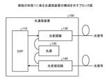
図1は、実施の形態1に係る光通信装置100の構成を示すブロック図である。図1に示す光通信装置100は、DSP(Digital Signal Processor)110、光源120、光変調器130及び光受信回路140を有する。
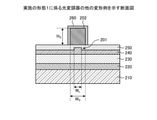
実施の形態2の特徴は、誘電体層に信号電極を埋設し、信号電極の側面を誘電体層によって被覆する点である。
120 光源
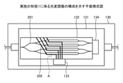
130 光変調器
131 光変調器チップ
132 光導波路基板
133 RF終端器
134 PBC
140 光受信回路
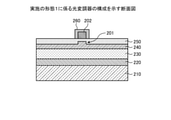
201 薄膜光導波路
202 信号電極
203 追加電極
210 LN基板
220 接地電極
230、250 バッファ層
240 薄膜LN基板
260 誘電体膜
270 誘電体層
Claims (8)
- 接地電位の接地電極と、
前記接地電極に積層される薄膜基板によって形成される薄膜光導波路と、
前記薄膜光導波路を挟んで前記接地電極と対向する位置に配置され、高周波信号を伝送する信号電極と、
前記信号電極の露出する表面の少なくとも一部を被覆する誘電体と
を有することを特徴とする光デバイス。 - 前記接地電極と前記薄膜基板の間に積層される第1のバッファ層と、
前記薄膜基板に積層され、前記薄膜光導波路を被覆する第2のバッファ層とをさらに有し、
前記信号電極は、
前記第2のバッファ層の表面の前記薄膜光導波路と重なる位置に配置される
ことを特徴とする請求項1記載の光デバイス。 - 前記信号電極は、
前記薄膜光導波路の幅よりも大きい幅を有する
ことを特徴とする請求項1記載の光デバイス。 - 前記信号電極は、
幅よりも高さが大きい断面形状を有する
ことを特徴とする請求項1記載の光デバイス。 - 前記誘電体は、
前記信号電極の側面と前記接地電極から遠い側の面とを被覆する誘電体膜を備える
ことを特徴とする請求項1記載の光デバイス。 - 前記誘電体は、
前記薄膜基板に積層される誘電体層を備え、
前記信号電極は、
前記誘電体層の前記薄膜光導波路と重なる位置に埋設される
ことを特徴とする請求項1記載の光デバイス。 - 前記信号電極は、
側面が前記誘電体によって被覆された第1の電極と、
前記第1の電極の前記接地電極から遠い側の面に接続し、前記第1の電極よりも幅広の第2の電極と
を有することを特徴とする請求項1記載の光デバイス。 - 電気信号に対する信号処理を実行するプロセッサと、
光を発生させる光源と、
前記プロセッサから出力される電気信号を用いて、前記光源から発生する光を変調する光デバイスとを有し、
前記光デバイスは、
接地電位の接地電極と、
前記接地電極に積層される薄膜基板によって形成される薄膜光導波路と、
前記薄膜光導波路を挟んで前記接地電極と対向する位置に配置され、高周波信号を伝送する信号電極と、
前記信号電極の露出する表面の少なくとも一部を被覆する誘電体とを有する
ことを特徴とする光通信装置。
Priority Applications (3)
| Application Number | Priority Date | Filing Date | Title |
|---|---|---|---|
| JP2020115650A JP2022013232A (ja) | 2020-07-03 | 2020-07-03 | 光デバイス及び光通信装置 |
| CN202110582615.XA CN113885227A (zh) | 2020-07-03 | 2021-05-27 | 光器件及光通信装置 |
| US17/334,040 US11719964B2 (en) | 2020-07-03 | 2021-05-28 | Optical device and optical communication device |
Applications Claiming Priority (1)
| Application Number | Priority Date | Filing Date | Title |
|---|---|---|---|
| JP2020115650A JP2022013232A (ja) | 2020-07-03 | 2020-07-03 | 光デバイス及び光通信装置 |
Publications (1)
| Publication Number | Publication Date |
|---|---|
| JP2022013232A true JP2022013232A (ja) | 2022-01-18 |
Family
ID=79010106
Family Applications (1)
| Application Number | Title | Priority Date | Filing Date |
|---|---|---|---|
| JP2020115650A Pending JP2022013232A (ja) | 2020-07-03 | 2020-07-03 | 光デバイス及び光通信装置 |
Country Status (3)
| Country | Link |
|---|---|
| US (1) | US11719964B2 (ja) |
| JP (1) | JP2022013232A (ja) |
| CN (1) | CN113885227A (ja) |
Cited By (2)
| Publication number | Priority date | Publication date | Assignee | Title |
|---|---|---|---|---|
| WO2023188195A1 (ja) * | 2022-03-30 | 2023-10-05 | 住友大阪セメント株式会社 | 光導波路素子及びそれを用いた光変調デバイス並びに光送信装置 |
| WO2025069276A1 (ja) * | 2023-09-27 | 2025-04-03 | 住友大阪セメント株式会社 | 光導波路素子及びそれを用いた光変調デバイス並びに光送信装置 |
Families Citing this family (2)
| Publication number | Priority date | Publication date | Assignee | Title |
|---|---|---|---|---|
| JP2022013232A (ja) * | 2020-07-03 | 2022-01-18 | 富士通オプティカルコンポーネンツ株式会社 | 光デバイス及び光通信装置 |
| CN119644614B (zh) * | 2025-01-10 | 2025-11-14 | 国科光芯金杏(北京)实验室科技有限公司 | 一种压电-热光复合调制器及其制备方法 |
Citations (7)
| Publication number | Priority date | Publication date | Assignee | Title |
|---|---|---|---|---|
| JP2008089936A (ja) * | 2006-09-30 | 2008-04-17 | Sumitomo Osaka Cement Co Ltd | 光制御素子 |
| WO2015087988A1 (ja) * | 2013-12-11 | 2015-06-18 | 住友大阪セメント株式会社 | 電気光学素子 |
| JP2015118371A (ja) * | 2013-11-15 | 2015-06-25 | Tdk株式会社 | 光変調器 |
| US20150309340A1 (en) * | 2014-04-24 | 2015-10-29 | International Business Machines Corporation | Waveguide structure |
| JP2019074595A (ja) * | 2017-10-13 | 2019-05-16 | Tdk株式会社 | 光変調器 |
| WO2019187335A1 (ja) * | 2018-03-30 | 2019-10-03 | 日本電気株式会社 | 光送受信装置、光変調器制御方法および光変調器制御プログラムを格納した非一時的なコンピュータ可読媒体 |
| JP2020020953A (ja) * | 2018-07-31 | 2020-02-06 | 富士通オプティカルコンポーネンツ株式会社 | 光変調器、光変調器モジュール、及び光送信モジュール |
Family Cites Families (12)
| Publication number | Priority date | Publication date | Assignee | Title |
|---|---|---|---|---|
| JP3021888B2 (ja) * | 1991-12-04 | 2000-03-15 | 住友金属鉱山株式会社 | 光導波路機能素子及びその製造方法 |
| JPH0954293A (ja) * | 1995-08-17 | 1997-02-25 | Sony Corp | 光導波路素子 |
| JP2836568B2 (ja) * | 1996-02-19 | 1998-12-14 | 日本電気株式会社 | 光制御素子及びその製造方法 |
| US6310700B1 (en) | 2000-09-15 | 2001-10-30 | Massachusetts Institute Of Technology | Velocity matching electrode structure for electro-optic modulators |
| JP2004227013A (ja) * | 2000-12-22 | 2004-08-12 | Nec Corp | 光導波路デバイス及びその製造方法 |
| JP2009098196A (ja) * | 2007-10-12 | 2009-05-07 | Fuji Xerox Co Ltd | 光導波路素子、及び光導波路素子のポーリング処理方法 |
| US8224143B2 (en) * | 2010-02-05 | 2012-07-17 | Advantest Corporation | Substrate structure and manufacturing method |
| JP5792702B2 (ja) | 2012-09-26 | 2015-10-14 | 住友大阪セメント株式会社 | 光変調器 |
| JP6221294B2 (ja) | 2013-03-28 | 2017-11-01 | 住友大阪セメント株式会社 | 光制御素子 |
| JP5983839B2 (ja) | 2015-08-06 | 2016-09-06 | 住友大阪セメント株式会社 | 光変調器 |
| JP6561383B2 (ja) * | 2017-03-31 | 2019-08-21 | 住友大阪セメント株式会社 | 光変調素子 |
| JP2022013232A (ja) * | 2020-07-03 | 2022-01-18 | 富士通オプティカルコンポーネンツ株式会社 | 光デバイス及び光通信装置 |
-
2020
- 2020-07-03 JP JP2020115650A patent/JP2022013232A/ja active Pending
-
2021
- 2021-05-27 CN CN202110582615.XA patent/CN113885227A/zh active Pending
- 2021-05-28 US US17/334,040 patent/US11719964B2/en active Active
Patent Citations (7)
| Publication number | Priority date | Publication date | Assignee | Title |
|---|---|---|---|---|
| JP2008089936A (ja) * | 2006-09-30 | 2008-04-17 | Sumitomo Osaka Cement Co Ltd | 光制御素子 |
| JP2015118371A (ja) * | 2013-11-15 | 2015-06-25 | Tdk株式会社 | 光変調器 |
| WO2015087988A1 (ja) * | 2013-12-11 | 2015-06-18 | 住友大阪セメント株式会社 | 電気光学素子 |
| US20150309340A1 (en) * | 2014-04-24 | 2015-10-29 | International Business Machines Corporation | Waveguide structure |
| JP2019074595A (ja) * | 2017-10-13 | 2019-05-16 | Tdk株式会社 | 光変調器 |
| WO2019187335A1 (ja) * | 2018-03-30 | 2019-10-03 | 日本電気株式会社 | 光送受信装置、光変調器制御方法および光変調器制御プログラムを格納した非一時的なコンピュータ可読媒体 |
| JP2020020953A (ja) * | 2018-07-31 | 2020-02-06 | 富士通オプティカルコンポーネンツ株式会社 | 光変調器、光変調器モジュール、及び光送信モジュール |
Cited By (2)
| Publication number | Priority date | Publication date | Assignee | Title |
|---|---|---|---|---|
| WO2023188195A1 (ja) * | 2022-03-30 | 2023-10-05 | 住友大阪セメント株式会社 | 光導波路素子及びそれを用いた光変調デバイス並びに光送信装置 |
| WO2025069276A1 (ja) * | 2023-09-27 | 2025-04-03 | 住友大阪セメント株式会社 | 光導波路素子及びそれを用いた光変調デバイス並びに光送信装置 |
Also Published As
| Publication number | Publication date |
|---|---|
| US20220004031A1 (en) | 2022-01-06 |
| CN113885227A (zh) | 2022-01-04 |
| US11719964B2 (en) | 2023-08-08 |
Similar Documents
| Publication | Publication Date | Title |
|---|---|---|
| US11719964B2 (en) | Optical device and optical communication device | |
| US10228605B2 (en) | Waveguide optical element | |
| JP7658184B2 (ja) | 光デバイス及び光通信装置 | |
| US9235066B2 (en) | Optical modulator | |
| JP7632166B2 (ja) | 光デバイス及び光通信装置 | |
| CN114185186B (zh) | 包括光调制器的光器件及光收发器 | |
| US20220163827A1 (en) | Optical device, optical communication apparatus, and manufacturing method of the optical device | |
| WO2007007604A1 (ja) | 光変調器 | |
| JP7585903B2 (ja) | 光デバイス、光通信装置及び光デバイスの製造方法 | |
| JP2004163859A (ja) | 光変調器 | |
| US6646776B1 (en) | Suppression of high frequency resonance in an electro-optical modulator | |
| JP7729080B2 (ja) | 光デバイス及び光通信装置 | |
| US20230258967A1 (en) | Optical waveguide device, optical modulator, optical modulation module, and optical transmission apparatus | |
| US6768570B2 (en) | Optical modulator | |
| JP2004226471A (ja) | 光変調素子および当該光変調素子を有するシステム | |
| US20250102840A1 (en) | Optical Waveguide Device, and Optical Modulation Device and Optical Transmission Apparatus Using Same | |
| KR20220072943A (ko) | 전기 광 변조기 | |
| JP2004245991A (ja) | 光導波路デバイスおよび光導波路デバイスと光伝送部材との結合構造 | |
| US20250199347A1 (en) | Electcro-optic modulator and a method for fabricating the electro-optic modulator | |
| US11320715B2 (en) | Optical device that includes optical modulator | |
| JP2010032690A (ja) | 光変調器 | |
| JP6394243B2 (ja) | 光導波路素子 | |
| JPH03204614A (ja) | 光変調器の製造方法 | |
| JP2004287354A (ja) | 光変調素子および当該光変調素子を有するシステム | |
| JPH03229215A (ja) | 光変調素子 |
Legal Events
| Date | Code | Title | Description |
|---|---|---|---|
| A621 | Written request for application examination |
Free format text: JAPANESE INTERMEDIATE CODE: A621 Effective date: 20230403 |
|
| A977 | Report on retrieval |
Free format text: JAPANESE INTERMEDIATE CODE: A971007 Effective date: 20231129 |
|
| A131 | Notification of reasons for refusal |
Free format text: JAPANESE INTERMEDIATE CODE: A131 Effective date: 20231205 |
|
| A521 | Request for written amendment filed |
Free format text: JAPANESE INTERMEDIATE CODE: A523 Effective date: 20240201 |
|
| A02 | Decision of refusal |
Free format text: JAPANESE INTERMEDIATE CODE: A02 Effective date: 20240416 |
|
| A521 | Request for written amendment filed |
Free format text: JAPANESE INTERMEDIATE CODE: A523 Effective date: 20240716 |
|
| A911 | Transfer to examiner for re-examination before appeal (zenchi) |
Free format text: JAPANESE INTERMEDIATE CODE: A911 Effective date: 20240723 |
|
| A912 | Re-examination (zenchi) completed and case transferred to appeal board |
Free format text: JAPANESE INTERMEDIATE CODE: A912 Effective date: 20240927 |