EP2071641A2 - Paquet de diode électroluminescente - Google Patents
Paquet de diode électroluminescente Download PDFInfo
- Publication number
- EP2071641A2 EP2071641A2 EP08075931A EP08075931A EP2071641A2 EP 2071641 A2 EP2071641 A2 EP 2071641A2 EP 08075931 A EP08075931 A EP 08075931A EP 08075931 A EP08075931 A EP 08075931A EP 2071641 A2 EP2071641 A2 EP 2071641A2
- Authority
- EP
- European Patent Office
- Prior art keywords
- electrodes
- pair
- led
- positive electrode
- encapsulant
- Prior art date
- Legal status (The legal status is an assumption and is not a legal conclusion. Google has not performed a legal analysis and makes no representation as to the accuracy of the status listed.)
- Ceased
Links
Images


Classifications
-
- H—ELECTRICITY
- H10—SEMICONDUCTOR DEVICES; ELECTRIC SOLID-STATE DEVICES NOT OTHERWISE PROVIDED FOR
- H10H—INORGANIC LIGHT-EMITTING SEMICONDUCTOR DEVICES HAVING POTENTIAL BARRIERS
- H10H20/00—Individual inorganic light-emitting semiconductor devices having potential barriers, e.g. light-emitting diodes [LED]
- H10H20/80—Constructional details
- H10H20/85—Packages
- H10H20/8506—Containers
-
- H—ELECTRICITY
- H05—ELECTRIC TECHNIQUES NOT OTHERWISE PROVIDED FOR
- H05K—PRINTED CIRCUITS; CASINGS OR CONSTRUCTIONAL DETAILS OF ELECTRIC APPARATUS; MANUFACTURE OF ASSEMBLAGES OF ELECTRICAL COMPONENTS
- H05K1/00—Printed circuits
- H05K1/18—Printed circuits structurally associated with non-printed electric components
- H05K1/181—Printed circuits structurally associated with non-printed electric components associated with surface mounted components
-
- H—ELECTRICITY
- H10—SEMICONDUCTOR DEVICES; ELECTRIC SOLID-STATE DEVICES NOT OTHERWISE PROVIDED FOR
- H10H—INORGANIC LIGHT-EMITTING SEMICONDUCTOR DEVICES HAVING POTENTIAL BARRIERS
- H10H20/00—Individual inorganic light-emitting semiconductor devices having potential barriers, e.g. light-emitting diodes [LED]
- H10H20/80—Constructional details
- H10H20/85—Packages
- H10H20/857—Interconnections, e.g. lead-frames, bond wires or solder balls
-
- H—ELECTRICITY
- H05—ELECTRIC TECHNIQUES NOT OTHERWISE PROVIDED FOR
- H05K—PRINTED CIRCUITS; CASINGS OR CONSTRUCTIONAL DETAILS OF ELECTRIC APPARATUS; MANUFACTURE OF ASSEMBLAGES OF ELECTRICAL COMPONENTS
- H05K2201/00—Indexing scheme relating to printed circuits covered by H05K1/00
- H05K2201/10—Details of components or other objects attached to or integrated in a printed circuit board
- H05K2201/10007—Types of components
- H05K2201/10106—Light emitting diode [LED]
-
- H—ELECTRICITY
- H05—ELECTRIC TECHNIQUES NOT OTHERWISE PROVIDED FOR
- H05K—PRINTED CIRCUITS; CASINGS OR CONSTRUCTIONAL DETAILS OF ELECTRIC APPARATUS; MANUFACTURE OF ASSEMBLAGES OF ELECTRICAL COMPONENTS
- H05K2201/00—Indexing scheme relating to printed circuits covered by H05K1/00
- H05K2201/10—Details of components or other objects attached to or integrated in a printed circuit board
- H05K2201/10431—Details of mounted components
- H05K2201/10507—Involving several components
- H05K2201/10522—Adjacent components
-
- H—ELECTRICITY
- H10—SEMICONDUCTOR DEVICES; ELECTRIC SOLID-STATE DEVICES NOT OTHERWISE PROVIDED FOR
- H10W—GENERIC PACKAGES, INTERCONNECTIONS, CONNECTORS OR OTHER CONSTRUCTIONAL DETAILS OF DEVICES COVERED BY CLASS H10
- H10W72/00—Interconnections or connectors in packages
- H10W72/50—Bond wires
- H10W72/551—Materials of bond wires
- H10W72/552—Materials of bond wires comprising metals or metalloids, e.g. silver
- H10W72/5522—Materials of bond wires comprising metals or metalloids, e.g. silver comprising gold [Au]
-
- H—ELECTRICITY
- H10—SEMICONDUCTOR DEVICES; ELECTRIC SOLID-STATE DEVICES NOT OTHERWISE PROVIDED FOR
- H10W—GENERIC PACKAGES, INTERCONNECTIONS, CONNECTORS OR OTHER CONSTRUCTIONAL DETAILS OF DEVICES COVERED BY CLASS H10
- H10W90/00—Package configurations
- H10W90/701—Package configurations characterised by the relative positions of pads or connectors relative to package parts
- H10W90/751—Package configurations characterised by the relative positions of pads or connectors relative to package parts of bond wires
- H10W90/756—Package configurations characterised by the relative positions of pads or connectors relative to package parts of bond wires between a chip and a stacked lead frame, conducting package substrate or heat sink
-
- Y—GENERAL TAGGING OF NEW TECHNOLOGICAL DEVELOPMENTS; GENERAL TAGGING OF CROSS-SECTIONAL TECHNOLOGIES SPANNING OVER SEVERAL SECTIONS OF THE IPC; TECHNICAL SUBJECTS COVERED BY FORMER USPC CROSS-REFERENCE ART COLLECTIONS [XRACs] AND DIGESTS
- Y02—TECHNOLOGIES OR APPLICATIONS FOR MITIGATION OR ADAPTATION AGAINST CLIMATE CHANGE
- Y02P—CLIMATE CHANGE MITIGATION TECHNOLOGIES IN THE PRODUCTION OR PROCESSING OF GOODS
- Y02P70/00—Climate change mitigation technologies in the production process for final industrial or consumer products
- Y02P70/50—Manufacturing or production processes characterised by the final manufactured product
Definitions
- the present invention generally relates to a light-emitting diode (LED) package. More particularly, the present invention relates to a leadframe type LED package.
- LED light-emitting diode
- LED packages Due to the advantages of long lifespan, no idling time, quick response speed (approximately 10 -9 seconds), compact volume, low power-consumption, low pollution, and high reliability, LED packages have been widely used in illumination apparatuses, back-lights of displays, or other electronic devices (e.g. traffic lights, cellular phones, scanners, fax machines, etc). Generally, LED packages are classified into top-view LED packages and side-view LED packages according to the orientation thereof.
- the chief-ray of the light emitted from the top-view LED package is substantially perpendicular to the circuit substrate; when the a side-view LED package is mounted onto a circuit substrate, the chief-ray of the light emitted from the side-view LED package is substantially parallel to the circuit substrate.
- the outlines of the top-view LED package and the side-view LED package are quite different, especially the design of electrodes (leads) exposed outside the LED packages.
- the designs of the circuit substrate or electrodes (leads) must be modified if the direction of the chief-ray is required to change.
- modification of circuit substrate or electrodes (leads) of the side-view LED package is not cost-effective and is unfavorable to mass production.
- the present invention is to provide an LED package favorable to mass production.
- the present invention provides an LED package including a leadframe having a pair of first electrodes and a pair of second electrodes, an LED chip disposed on the leadframe, and an encapsulant encapsulating a portion of the leadframe and the LED chip.
- the pair of first electrodes and the pair of second electrodes are electrically connected with the LED chip.
- the pair of first electrodes and the pair of second electrodes are located outside the encapsulant.
- the encapsulant has a top surface, a bottom surface, a first side surface and a second side surface opposite to the first side surface, wherein the pair of first electrodes extend from the first side surface to the bottom surface, and the pair of second electrodes extend from the second side surface to the bottom surface.
- the pair of first electrodes include a first positive electrode and a first negative electrode electrically insulated from the first positive electrode
- the pair of second electrodes include a second positive electrode and a second negative electrode electrically insulated from the second positive electrode.
- the first positive electrode is electrically connected with the second positive electrode while the first negative electrode is electrically connected with the second negative electrode.
- the leadframe has a first connecting conductor and a second connecting conductor, the first connecting conductor is electrically connected between the first positive electrode and the second positive electrode, while the second connecting conductor is electrically connected between the first negative electrode and the second negative electrode.
- the first connecting conductor and the second connecting conductor are encapsulated by the encapsulant.
- the encapsulant has an identification mark for identifying the first positive electrode and the second positive electrode.
- each first electrode is bent to extend along the first side surface and the bottom surface
- each second electrode is bent to extend along the second side surface and the bottom surface
- the encapsulant includes a housing having a cavity and a transparent material layer disposed in the cavity, wherein the LED chip and a portion of the leadframe in the cavity is encapsulated by the transparent material layer.
- the housing is opaque.
- the transparent material layer has phosphor distributed therein.
- a material of the housing is an insulating material.
- a material of the transparent material layer is an insulating material.
- the encapsulant has a first protruding portion located on the first side surface such that the pair of first electrodes are separated by the first protruding portion.
- the encapsulant has a second protruding portion located on the second side surface such that the pair of second electrodes are separated by the second protruding portion.
- the encapsulant has a third side surface and a fourth side surface opposite to the third side surface, the encapsulant has at least one recess located on the third side surface and/or the fourth side surface.
- the present invention provides an light-emitting diode (LED) module including a circuit substrate and a plurality of LED packages mentioned above, wherein the LED packages are disposed on the circuit substrate.
- LED light-emitting diode
- the LED packages are arranged in at least one row so as to provide at least one linear light source.
- the pair of first electrodes comprise a first positive electrode and a first negative electrode electrically insulated from the first positive electrode
- the pair of second electrodes comprise a second positive electrode and a second negative electrode electrically insulated from the second positive electrode.
- the circuit substrate has at least one positive connection pad and at least one negative connection pads, the positive connection pad between two adjacent LED packages is electrically connected with the first positive electrode and the second positive electrode simultaneously, and the negative connection pad between two adjacent LED packages is electrically connected with the first negative electrode and the second negative electrode simultaneously
- the LED package of the present invention is capable of functioning as a top-view LED package or a side-view LED package without modifying the design of electrodes, the LED package of the present invention is favorable to mass production.
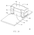
- Fig. 1 is a schematic view illustrating an LED package according to an embodiment of the present invention.
- Fig. 2A to Fig. 2D are schematic views illustrating an LED array having at least one top-view LED package according to an embodiment of the present invention.
- Fig. 3A to Fig. 3C are schematic views illustrating an LED array having at least one side-view LED package according to an embodiment of the present invention.
- Fig 4 is a schematic view illustrating two mounting orientations of the side-view LED packages on a circuit substrate according to an embodiment of the present invention.
- Fig 5 is a top view illustrating an arrangement of the side-view LED packages on a circuit substrate according to an embodiment of the present invention.
- Fig 6 is a top view illustrating an arrangement of the side-view LED packages on a circuit substrate according to another embodiment of the present invention.
- Fig. 1 is a schematic view illustrating an LED package according to an embodiment of the present invention.
- the LED package 100 of the embodiment includes a leadframe 110, an LED chip 120 disposed on the leadframe 110, and an encapsulant 130 encapsulating a portion of the leadframe 110 and the LED chip 120.
- the leadframe 110 has a pair of first electrodes 112 and a pair of second electrodes 114.
- the pair of first electrodes 112 and the pair of second electrodes 114 are electrically connected with the LED chip 120.
- the pair of first electrodes 112 and the pair of second electrodes 114 are located outside the encapsulant 130.
- the encapsulant 130 has a top surface 130a, a bottom surface 130b, a first side surface 130c and a second side surface 130d opposite to the first side surface 130c, wherein the pair of first electrodes 112 extend from the first side surface 130c to the bottom surface 130b, and the pair of second electrodes 114 extend from the second side surface 130d to the bottom surface 130b. Since the pair of first electrodes 112 and the pair of second electrodes 114 are exposed outside the encapsulant 130, heat generated from the LED chip 120 is conducted through the pair of first electrodes 112 and the pair of second electrodes 114 simultaneously and is dissipated rapidly via heat exchange. Accordingly, the LED package 100 having two pairs of electrodes (i.e. the first electrodes 112 and the second electrodes 114) exposed outside the encapsulant 130 has enhanced heat dissipation performance.
- the LED package 100 is capable of serving as a top-view LED package or a side-view LED package without modifying the electrode design thereof, since each first electrode 112 is bent to extend along the first side surface 130c and the bottom surface 130b, and each second electrode 114 is bent to extend along the second side surface 130d and the bottom surface 130b.
- the pair of first electrodes 112 of the embodiment include a first positive electrode 112a and a first negative electrode 112b electrically insulated from the first positive electrode 112a, while the pair of second electrodes 114 include a second positive electrode 114a and a second negative electrode 114b electrically insulated from the second positive electrode 114a.
- the first positive electrode 112a is electrically connected with the second positive electrode 114a while the first negative electrode 112b is electrically connected with the second negative electrode 114b.
- the leadframe 110 has a first connecting conductor 116 and a second connecting conductor 118, the first connecting conductor 116 is electrically connected between the first positive electrode 112a and the second positive electrode 114a, while the second connecting conductor 118 is electrically connected between the first negative electrode 112b and the second negative electrode 114b.
- the leadframe 110 having the first electrodes 112, the second electrodes 114, the first connecting conductor 116, and the second connecting conductor 118 are formed by metal, such as copper, silver, or gold.
- the first connecting conductor 116 and the second connecting conductor 118 are encapsulated by the encapsulant 130.
- the first connecting conductor 116 may serve as a die pad for carrying the LED chip 120 while the second connecting conductor 118 may serve as a wire-bonding pad such that the LED chip 120 is electrically connected with the second connecting conductor 118 via a bonding wire 140.
- the bonding wire 140 may be a gold wire formed by wire bonder.
- the electrical connection between the LED chip 120 and the leadframe 110 shown in Fig. 1 is merely for illustration; in other words, the LED chip 120 and the leadframe 110 may be electrically connected through more than one bonding wires or conductive bumps.
- the LED chip 120 may be a chip of any configuration, the number of pad(s) of the LED chip 120 for electrically connecting with the leadframe 110 may be one or more than one.
- the encapsulant 130 includes a housing 132 having a cavity 132a and a transparent material layer 134 disposed in the cavity 132a of the housing 132, wherein the LED chip 120 and a portion of the leadframe 110 in the cavity 132a is encapsulated by the transparent material layer 134.
- the housing 132 is opaque so as to confine the propagation direction of the light emitted from the LED chip 120.
- the material of the housing 132 and the transparent material layer 134 is an insulating material.
- the transparent material layer 134 has yellow phosphor (e.g. yttrium aluminum garnet) distributed therein when the LED chip 120 disposed within the cavity 132a of the housing 132 is an LED chip for emitting blue light.
- the transparent material layer 134 has at least one kind of phosphor capable of being excited and emits required color light (e.g. red, green, and/or blue light, etc) distributed therein when the LED chip 120 disposed within the cavity 132a of the housing 132 is an LED chip for emitting light with short wavelength (e.g. ultraviolet light).
- the encapsulant 130 of the embodiment has an identification mark 136 for identifying the first positive electrode 112a and the second positive electrode 114a.
- the identification mark 136 is helpful to differentiate the first positive electrode 112a from the first negative electrode 112b, or differentiate the second positive electrode 114a from the second negative electrode 114b.
- the identification mark 136 may be formed at a corner of the encapsulant 130, or other proper positions.
- a first protruding portion P1 may be formed on the first side surface 130c of the encapsulant 130 such that the pair of first electrodes 112 (i.e. the first positive electrode 112a and the first negative electrode 112b) are physically separated by the first protruding portion P1.
- a second protruding portion P2 may be formed on the second side surface 130d of the encapsulant 130 such that the pair of second electrodes 114 (i.e. the second positive electrode 114a and the second negative electrode 114b) are physically separated by the second protruding portion P2.
- the encapsulant 130 has a third side surface 130e and a fourth side surface 130f opposite to the third side surface 130e, the encapsulant 130 has at least one recess R located on the third side surface 130e. It is noted that the recess R may be formed on the fourth side surface 310f, or on both the third side surface 130e and the fourth side surface 310f. In detail, an edge of the leadframe 110 is exposed by the recess R of the encapsulant 130.
- FIG. 2A to Fig. 2D are schematic views illustrating an LED array having at least one top-view LED package according to an embodiment of the present invention.
- an LED array 200 of the present embodiment includes a circuit substrate 210 and a plurality of LED packages 100 (only one LED package 100 is shown in Fig. 2A to Fig. 2D ).
- the LED package 100 is disposed on the circuit substrate 210 having a positive connection pad 212a and a negative connection pad 212b, wherein the first positive electrode 112a and the second positive electrode 114a are electrically connected with the positive connection pad 212a via a solder material S1, and the first negative electrode 112b and the second negative electrode 114b are electrically connected with the negative connection pad 212b via a solder material S2. It is noted that the first positive electrode 112a, the first negative electrode 112b, the second positive electrode 114a, and the second negative electrode 114b are all bonded with the circuit substrate 210 via the solder material S1 and S2, the bonding strength between the LED package 100 and the circuit substrate 210 is strong accordingly.
- the LED packages 100 is functioned as a side-view LED package, since the chief-ray C of the light emitted from the LED package 100 is substantially perpendicular to the circuit substrate 210.
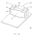
- FIG. 3A to Fig. 3C are schematic views illustrating an LED array having at least one top-view LED package according to an embodiment of the present invention.
- an LED array 200' of the present embodiment includes a circuit substrate 210 and a plurality of LED packages 100 (only one LED package 100 is shown in Fig. 3A to Fig. 3C ).
- the LED package 100 is disposed on the circuit substrate 210 having a positive connection pad 212a and a negative connection pad 212b, wherein only the first positive electrode 112a is electrically connected with the positive connection pad 212a via a solder material S1, and only the first negative electrode 112b is electrically connected with the negative connection pad 212b via a solder material S2.
- the LED packages 100 is functioned as a side-view LED package, since the chief-ray C of the light emitted from the LED package 100 is substantially parallel to the circuit substrate 210.
- the LED packages 100 may be mounted onto the circuit substrate 210 in different orientations so as to provide side-view illumination or top-view illumination.
- Fig 4 is a schematic view illustrating two mounting orientations of the side-view LED packages on a circuit substrate according to an embodiment of the present invention.
- the first positive electrode 112a is electrically connected with the positive connection pad 212a via the solder material S1 while the first negative electrode 112b is electrically connected with the negative connection pad 212b via the solder material S2, such that the LED package 110 can provide a light propagating along a predetermined direction (shown in the left part of Fig. 4 ).
- different circuit substrates may have different layouts, for example, positions of the positive connection pad 212a and the negative connection pad 212b may be interchanges (shown in the right part of Fig.
- the LED package 110 may be flipped and mounted onto the circuit substrate 210' such that the second positive electrode 114a is electrically connected with the positive connection pad 212a via the solder material S1 while the second negative electrode 114b is electrically connected with the negative connection pad 212b via the solder material S2.
- the LED package 100 mounted on the circuit substrate 210 and the LED package 100 mounted on the circuit substrate 210' are capable of providing light with the same propagating direction.
- Fig 5 is a top view illustrating an arrangement of the side-view LED packages on a circuit substrate according to an embodiment of the present invention.
- an LED module including a circuit substrate 210 and a plurality of LED packages 100 disposed on the circuit substrate 210 is provided, wherein the LED packages 100 on the circuit substrate 210 are arranged in one row so as to provide a linear light source.
- Each positive connection pad 212a between two adjacent LED packages 100 is electrically connected with the first positive electrode 112a and the second positive electrode 114a simultaneously.
- Each negative connection pad 212b between two adjacent LED packages 100 is electrically connected with the first negative electrode 112b and the second negative electrode 114b simultaneously.
- Fig 6 is a top view illustrating an arrangement of the side-view LED packages on a circuit substrate according to another embodiment of the present invention.
- an LED module including a circuit substrate 210 and a plurality of LED packages 100 disposed on the circuit substrate 210 is provided, wherein the LED packages 100 on the circuit substrate 210 are arranged in two rows so as to provide two linear light sources.
- Each positive connection pad 212a between two adjacent LED packages 100 is electrically connected with two first positive electrodes 112a and two second positive electrodes 114a simultaneously.
- Each negative connection pad 212b between two adjacent LED packages 100 is electrically connected with two first negative electrodes 112b and two second negative electrodes 114b simultaneously.
- the LED packages 100 can be arranged more compact.
- the LED package of the present invention is capable of being mounted on the circuit substrate in various orientations so as to provide side-view illumination or top-view illumination.
Landscapes
- Engineering & Computer Science (AREA)
- Microelectronics & Electronic Packaging (AREA)
- Led Device Packages (AREA)
Applications Claiming Priority (1)
| Application Number | Priority Date | Filing Date | Title |
|---|---|---|---|
| TW096220959U TWM337834U (en) | 2007-12-10 | 2007-12-10 | Package structure for light emitting diode |
Publications (2)
| Publication Number | Publication Date |
|---|---|
| EP2071641A2 true EP2071641A2 (fr) | 2009-06-17 |
| EP2071641A3 EP2071641A3 (fr) | 2013-10-09 |
Family
ID=40456858
Family Applications (1)
| Application Number | Title | Priority Date | Filing Date |
|---|---|---|---|
| EP08075931.9A Ceased EP2071641A3 (fr) | 2007-12-10 | 2008-12-10 | Paquet de diode électroluminescente |
Country Status (4)
| Country | Link |
|---|---|
| US (1) | US8138517B2 (fr) |
| EP (1) | EP2071641A3 (fr) |
| JP (1) | JP2009141370A (fr) |
| TW (1) | TWM337834U (fr) |
Cited By (2)
| Publication number | Priority date | Publication date | Assignee | Title |
|---|---|---|---|---|
| WO2014048834A1 (fr) * | 2012-09-27 | 2014-04-03 | Osram Opto Semiconductors Gmbh | Boîtier pour un composant optoélectronique, module électronique, procédé de fabrication de boîtiers et procédé de fabrication de modules électroniques |
| WO2019002098A1 (fr) * | 2017-06-30 | 2019-01-03 | Osram Opto Semiconductors Gmbh | Composant à semi-conduteur optoélectronique et système comprenant un composant à semi-conduteur optoélectronique |
Families Citing this family (7)
| Publication number | Priority date | Publication date | Assignee | Title |
|---|---|---|---|---|
| US20100237364A1 (en) * | 2009-03-19 | 2010-09-23 | Christy Alexander C | Thermal Energy Dissipating and Light Emitting Diode Mounting Arrangement |
| US9759727B2 (en) * | 2010-03-23 | 2017-09-12 | Massachusetts Institute Of Technology | Ligands for semiconductor nanocrystals |
| TW201330332A (zh) * | 2012-01-02 | 2013-07-16 | 隆達電子股份有限公司 | 固態發光元件及其固態發光封裝體 |
| US9105825B2 (en) | 2013-06-03 | 2015-08-11 | Avago Technologies General Ip (Singapore) Pte. Ltd. | Light source package and method of manufacturing the same |
| JP6102670B2 (ja) * | 2013-10-07 | 2017-03-29 | 豊田合成株式会社 | 発光装置 |
| US11307434B2 (en) * | 2016-09-01 | 2022-04-19 | 3D Live, Inc. | Stereoscopic display apparatus employing light emitting diodes with polarizing film/lens materials |
| US11914141B1 (en) | 2018-08-23 | 2024-02-27 | Apple Inc. | Electronic device with protected light sources |
Citations (1)
| Publication number | Priority date | Publication date | Assignee | Title |
|---|---|---|---|---|
| KR20060010578A (ko) * | 2004-07-28 | 2006-02-02 | 삼성전기주식회사 | 광장치용 led 패키지 및 어셈블리 |
Family Cites Families (22)
| Publication number | Priority date | Publication date | Assignee | Title |
|---|---|---|---|---|
| JPH05243442A (ja) * | 1992-02-27 | 1993-09-21 | Nec Corp | 表面実装型ダイオード |
| DE4446566A1 (de) * | 1994-12-24 | 1996-06-27 | Telefunken Microelectron | Mehrpoliges, oberflächenmontierbares, elektronisches Bauelement |
| JP3993302B2 (ja) * | 1998-05-20 | 2007-10-17 | ローム株式会社 | 半導体装置 |
| KR100378917B1 (ko) * | 1998-05-20 | 2003-04-07 | 로무 가부시키가이샤 | 반도체장치 |
| JP4028101B2 (ja) | 1998-05-20 | 2007-12-26 | ローム株式会社 | 半導体装置 |
| JP2002222993A (ja) * | 2001-01-23 | 2002-08-09 | Rohm Co Ltd | 半導体発光素子 |
| JP4631175B2 (ja) * | 2001-01-26 | 2011-02-16 | 日亜化学工業株式会社 | パッケージ成形体と発光装置 |
| JP2002223005A (ja) | 2001-01-26 | 2002-08-09 | Toyoda Gosei Co Ltd | 発光ダイオード及びディスプレイ装置 |
| JP4066608B2 (ja) * | 2001-03-16 | 2008-03-26 | 日亜化学工業株式会社 | パッケージ成形体及びその製造方法 |
| JP2004214380A (ja) * | 2002-12-27 | 2004-07-29 | Polyplastics Co | リードフレーム形成用金属箔、電子部品用パッケージ、その製造方法、及び表面実装型発光部品 |
| JP2005191530A (ja) | 2003-12-03 | 2005-07-14 | Sumitomo Electric Ind Ltd | 発光装置 |
| JP2005260276A (ja) * | 2003-12-03 | 2005-09-22 | Sumitomo Electric Ind Ltd | 発光装置 |
| KR100665298B1 (ko) * | 2004-06-10 | 2007-01-04 | 서울반도체 주식회사 | 발광장치 |
| JP4789433B2 (ja) * | 2004-06-30 | 2011-10-12 | 三洋電機株式会社 | Led表示器用筺体及びled表示器 |
| JP2006024794A (ja) * | 2004-07-08 | 2006-01-26 | Sanyo Electric Co Ltd | フルカラー発光ダイオード装置 |
| KR101241650B1 (ko) * | 2005-10-19 | 2013-03-08 | 엘지이노텍 주식회사 | 엘이디 패키지 |
| KR100741821B1 (ko) * | 2006-02-23 | 2007-07-23 | 삼성전기주식회사 | 발광 다이오드 모듈 |
| JP2008166782A (ja) * | 2006-12-26 | 2008-07-17 | Seoul Semiconductor Co Ltd | 発光素子 |
| US7800304B2 (en) * | 2007-01-12 | 2010-09-21 | Avago Technologies Ecbu Ip (Singapore) Pte. Ltd. | Multi-chip packaged LED light source |
| JP4689637B2 (ja) * | 2007-03-23 | 2011-05-25 | シャープ株式会社 | 半導体発光装置 |
| JP5179106B2 (ja) * | 2007-07-13 | 2013-04-10 | ローム株式会社 | 半導体発光装置 |
| WO2009101718A1 (fr) * | 2008-02-13 | 2009-08-20 | Canon Components, Inc. | Diode émettant de la lumière blanche, dispositif émetteur de lumière blanche, et dispositif d'éclairage de type linéaire les utilisant |
-
2007
- 2007-12-10 TW TW096220959U patent/TWM337834U/zh unknown
-
2008
- 2008-12-10 JP JP2008314885A patent/JP2009141370A/ja active Pending
- 2008-12-10 US US12/331,452 patent/US8138517B2/en not_active Expired - Fee Related
- 2008-12-10 EP EP08075931.9A patent/EP2071641A3/fr not_active Ceased
Patent Citations (1)
| Publication number | Priority date | Publication date | Assignee | Title |
|---|---|---|---|---|
| KR20060010578A (ko) * | 2004-07-28 | 2006-02-02 | 삼성전기주식회사 | 광장치용 led 패키지 및 어셈블리 |
Cited By (3)
| Publication number | Priority date | Publication date | Assignee | Title |
|---|---|---|---|---|
| WO2014048834A1 (fr) * | 2012-09-27 | 2014-04-03 | Osram Opto Semiconductors Gmbh | Boîtier pour un composant optoélectronique, module électronique, procédé de fabrication de boîtiers et procédé de fabrication de modules électroniques |
| WO2019002098A1 (fr) * | 2017-06-30 | 2019-01-03 | Osram Opto Semiconductors Gmbh | Composant à semi-conduteur optoélectronique et système comprenant un composant à semi-conduteur optoélectronique |
| US11393962B2 (en) | 2017-06-30 | 2022-07-19 | Osram Oled Gmbh | Optoelectronic semiconductor component and assembly having an optoelectronic semiconductor component |
Also Published As
| Publication number | Publication date |
|---|---|
| EP2071641A3 (fr) | 2013-10-09 |
| JP2009141370A (ja) | 2009-06-25 |
| US8138517B2 (en) | 2012-03-20 |
| US20090146157A1 (en) | 2009-06-11 |
| TWM337834U (en) | 2008-08-01 |
Similar Documents
| Publication | Publication Date | Title |
|---|---|---|
| US9472743B2 (en) | Light emitting diode package | |
| US8138517B2 (en) | Light-emitting diode package | |
| US10950759B2 (en) | LED module | |
| EP2187459B1 (fr) | Dispositif électroluminescent | |
| CN104916770B (zh) | 发光二极管装置 | |
| US7935982B2 (en) | Side view type LED package | |
| KR101360732B1 (ko) | 발광 다이오드 패키지 | |
| EP2372801A2 (fr) | Sous-montages pour paquets de dispositif électroluminescent semi-conducteur et paquets de dispositif électroluminescent semi-conducteur les incluant | |
| EP2381474A2 (fr) | Cadre en plomb pour paquet de dispositif électroluminescent, paquet de dispositif électroluminescent et appareil d'éclairage utilisant le paquet de dispositif électroluminescent | |
| JP2009177187A (ja) | 発光ダイオードパッケージ | |
| CN1961431A (zh) | 表面安装型发光芯片封装件 | |
| CN102479910A (zh) | Led模块 | |
| EP2341560A2 (fr) | Dispositif électroluminescent et son procédé de fabrication | |
| CN105514249A (zh) | 发光二极管封装以及承载板 | |
| CN102478172A (zh) | 照明装置 | |
| CN103545431B (zh) | 发光装置 | |
| US9502618B2 (en) | LED module | |
| KR100937136B1 (ko) | 복수의 패키지를 모듈화한 리드프레임을 이용한 발광다이오드 모듈 | |
| CN103748701A (zh) | 发光装置 | |
| KR101374894B1 (ko) | 양면 발광형 발광 다이오드 패키지 | |
| TWI531096B (zh) | 側面發光型發光二極體封裝結構及其製造方法 | |
| US9887179B2 (en) | Light emitting diode device and light emitting device using the same | |
| CN102086996B (zh) | Led侧立式背光源 |
Legal Events
| Date | Code | Title | Description |
|---|---|---|---|
| PUAI | Public reference made under article 153(3) epc to a published international application that has entered the european phase |
Free format text: ORIGINAL CODE: 0009012 |
|
| AK | Designated contracting states |
Kind code of ref document: A2 Designated state(s): AT BE BG CH CY CZ DE DK EE ES FI FR GB GR HR HU IE IS IT LI LT LU LV MC MT NL NO PL PT RO SE SI SK TR |
|
| AX | Request for extension of the european patent |
Extension state: AL BA MK RS |
|
| PUAL | Search report despatched |
Free format text: ORIGINAL CODE: 0009013 |
|
| AK | Designated contracting states |
Kind code of ref document: A3 Designated state(s): AT BE BG CH CY CZ DE DK EE ES FI FR GB GR HR HU IE IS IT LI LT LU LV MC MT NL NO PL PT RO SE SI SK TR |
|
| AX | Request for extension of the european patent |
Extension state: AL BA MK RS |
|
| RIC1 | Information provided on ipc code assigned before grant |
Ipc: H01L 33/00 20100101AFI20130902BHEP |
|
| 17P | Request for examination filed |
Effective date: 20140331 |
|
| RBV | Designated contracting states (corrected) |
Designated state(s): AT BE BG CH CY CZ DE DK EE ES FI FR GB GR HR HU IE IS IT LI LT LU LV MC MT NL NO PL PT RO SE SI SK TR |
|
| AKX | Designation fees paid |
Designated state(s): AT BE BG CH CY CZ DE DK EE ES FI FR GB GR HR HU IE IS IT LI LT LU LV MC MT NL NO PL PT RO SE SI SK TR |
|
| 17Q | First examination report despatched |
Effective date: 20150810 |
|
| APBK | Appeal reference recorded |
Free format text: ORIGINAL CODE: EPIDOSNREFNE |
|
| APBN | Date of receipt of notice of appeal recorded |
Free format text: ORIGINAL CODE: EPIDOSNNOA2E |
|
| APBR | Date of receipt of statement of grounds of appeal recorded |
Free format text: ORIGINAL CODE: EPIDOSNNOA3E |
|
| APAF | Appeal reference modified |
Free format text: ORIGINAL CODE: EPIDOSCREFNE |
|
| APBT | Appeal procedure closed |
Free format text: ORIGINAL CODE: EPIDOSNNOA9E |
|
| 18R | Application refused |
Effective date: 20181007 |