EP2073397B1 - Datenflusssteuerung in Hochgeschwindigkeits-Abwärtsstrecken-Paketzugang (HSDPA) - Google Patents
Datenflusssteuerung in Hochgeschwindigkeits-Abwärtsstrecken-Paketzugang (HSDPA) Download PDFInfo
- Publication number
- EP2073397B1 EP2073397B1 EP08171811.6A EP08171811A EP2073397B1 EP 2073397 B1 EP2073397 B1 EP 2073397B1 EP 08171811 A EP08171811 A EP 08171811A EP 2073397 B1 EP2073397 B1 EP 2073397B1
- Authority
- EP
- European Patent Office
- Prior art keywords
- data
- processing module
- data processing
- module
- hsdpa
- Prior art date
- Legal status (The legal status is an assumption and is not a legal conclusion. Google has not performed a legal analysis and makes no representation as to the accuracy of the status listed.)
- Ceased
Links
Images



Classifications
-
- H—ELECTRICITY
- H04—ELECTRIC COMMUNICATION TECHNIQUE
- H04B—TRANSMISSION
- H04B1/00—Details of transmission systems, not covered by a single one of groups H04B3/00 - H04B13/00; Details of transmission systems not characterised by the medium used for transmission
- H04B1/69—Spread spectrum techniques
- H04B1/707—Spread spectrum techniques using direct sequence modulation
- H04B1/7097—Interference-related aspects
- H04B1/7103—Interference-related aspects the interference being multiple access interference
- H04B1/7105—Joint detection techniques, e.g. linear detectors
- H04B1/71055—Joint detection techniques, e.g. linear detectors using minimum mean squared error [MMSE] detector
-
- H—ELECTRICITY
- H04—ELECTRIC COMMUNICATION TECHNIQUE
- H04B—TRANSMISSION
- H04B1/00—Details of transmission systems, not covered by a single one of groups H04B3/00 - H04B13/00; Details of transmission systems not characterised by the medium used for transmission
- H04B1/69—Spread spectrum techniques
- H04B1/707—Spread spectrum techniques using direct sequence modulation
- H04B1/7097—Interference-related aspects
- H04B1/7103—Interference-related aspects the interference being multiple access interference
- H04B1/7105—Joint detection techniques, e.g. linear detectors
-
- H—ELECTRICITY
- H04—ELECTRIC COMMUNICATION TECHNIQUE
- H04B—TRANSMISSION
- H04B2201/00—Indexing scheme relating to details of transmission systems not covered by a single group of H04B3/00 - H04B13/00
- H04B2201/69—Orthogonal indexing scheme relating to spread spectrum techniques in general
- H04B2201/707—Orthogonal indexing scheme relating to spread spectrum techniques in general relating to direct sequence modulation
- H04B2201/70707—Efficiency-related aspects
- H04B2201/7071—Efficiency-related aspects with dynamic control of receiver resources
- H04B2201/70711—Efficiency-related aspects with dynamic control of receiver resources with modular structure
-
- H—ELECTRICITY
- H04—ELECTRIC COMMUNICATION TECHNIQUE
- H04J—MULTIPLEX COMMUNICATION
- H04J13/00—Code division multiplex systems
- H04J13/0077—Multicode, e.g. multiple codes assigned to one user
Definitions
- This document generally relates to wireless communication systems.
- first generation (1G) used analog technology called frequency division multiple access (FDMA) to deliver a radio-based voice channel to a mobile telephone user.
- second generation (2G) systems were deployed using digital technologies.
- the first U.S. system used time division multiple access (TDMA).
- TDMA technology was used to introduce the Global System for Mobile Communication (GSM) to Europe.
- CDMA code division multiple access
- IS-95 Interim Standard-95
- Wideband CDMA is a transmission technology for 3G (third generation) Universal Mobile Telecommunications System (UMTS) mobile or wireless communication.
- WCDMA systems support voice and data transmission with variable data rates in wireless communication channels such as random access channels, paging channels, broadcast channels, etc.
- WCDMA systems contain one or several radio frequency carriers. Each radio frequency carrier contains a number of spreading codes which may be allocated to provide different data rates to satisfy different mobile user requirements.
- WCDMA systems often utilize transport channels which may be mapped to physical channels.
- the physical layer/channel (layer 1) is the lowest layer in the OSI Reference Model and it supports functions used for the transmission of bit streams on the physical medium.
- the physical layer subsequently provides data transport services to higher layers of the wireless communication system. Characteristics of a transport channel are defined by its transport format (or format set), specifying the physical layer processing to be applied to the transport channel in question, such as convolutional channel coding and interleaving, and any service-specific rate matching as may be needed.
- Transport channels may represent services offered by Layer 1 to the higher layers.
- Exemplary transport channels include: a) common transport channels such as BCH (broadcast channel, often used as a downlink (DL) transport channel to broadcast system and/or cell specific information), FACH (forward access channel), PCH (paging channel), RACH (random access channel), CPCH (common packet channel), and DSCH (downlink shared channel), and b) dedicated channels (DCH) which may be used on the uplink or downlink.
- BCH broadcast channel, often used as a downlink (DL) transport channel to broadcast system and/or cell specific information
- FACH forward access channel
- PCH paging channel
- RACH random access channel
- CPCH common packet channel
- DSCH downlink shared channel
- DCH dedicated channels
- TD-SCDMA Time Division Synchronous Code Division Multiple Access
- 3G third generation
- Universal Mobile Telecommunications System UMTS
- TD-SCDMA uses time domain duplexing in combination with code domain multiple access techniques to support both symmetrical and asymmetrical traffic.
- High speed downlink packet access is an important feature of Release 5 of the third Generation Partnership Project (3GPP) specification and represents the first step in the evolution of TD-SCDMA toward high data rates. More specifically, HSDPA is a UMTS enhancement to provide increased downlink data rates that is defined in Release 5 of the UMTS specifications. The HSDPA is expected to increase system capacity, reduce roundtrip delay and increase peak data rates to more than 2.0 megabits per second. A new shared channel called high speed downlink shared channel (HS-DSCH) has been introduced to support the above goals.
- 3GPP Third Generation Partnership Project
- the baseband receiver includes two main components: an inner receiver, also known as an equalizer or a chip rate processor, which mitigates the effects of multi-path and interference, and an outer receiver which performs channel decoding and other symbol rate processing.
- an inner receiver also known as an equalizer or a chip rate processor, which mitigates the effects of multi-path and interference
- an outer receiver which performs channel decoding and other symbol rate processing.
- Document WO2008/042210 which falls under Article 54(3) EPC, discloses a method for controlling data flow in a wireless communication system, comprising: - receiving data in a joint-detection accelerator (JDA) front-end module implemented in hardware; - enabling a JDA back-end module when at least one signal time slot of the received data comprises data that complies with a first data transmission standard; - exchanging signals between the first data processing module and software executing in a processor (DSP) to indicate that the first data processing module is ready to transmit data to the second data processing module; - processing the data in the second data processing module for the at least one signal time slot; and - enabling a bit rate processing module upon a completion of processing at least one data block in the second data processing module, the at least one data block comprising multiple signal time slots.
- JDA joint-detection accelerator
- DSP processor
- a method for controlling data flow in a wireless communication system includes receiving data in a first data processing module; enabling a second data processing module when at least one signal time slot of the received data comprises data that complies with a first data transmission standard; exchanging signals between the first data processing module and software executing in a processor to indicate that the first data processing module is ready to transmit data to the second data processing module, and determining that a software configuration of the second data processing module has been completed; processing the data in the second data processing module for the at least one signal time slot; and enabling a third data processing module upon a completion of processing at least one data block in the second data processing module, and determining that a software configuration of the third data processing module has been completed, the at least one data block comprising multiple signal time slots.
- the first data transmission standard may comprise high speed downlink packet access (HSDPA).
- the first data processing module may include a joint detection accelerator comprising a first-in, first-out (FIFO) module.
- the second data processing module may process and convert output data from the first data processing module into a format suitable for the third data processing module.
- the first data processing module may be configured to: extract data that complies with a second data transmission standard, and process the data in the second data transmission standard by software executing in a processor.
- the third data processing module may include a bit rate processor.
- the software executing on a processor may provide a constellation gain value to the second data processing module.
- the second data processing module is configured to provide a sigmal-to-interference-and-noise-ratio (SINR) value.
- SINR value may be computed on a time slot basis.
- the third data processing module may include a bit rate processor.
- an apparatus for controlling data flow in a wireless communication system includes a first data processing module that receives data; circuitry to indicate that the first data processing module is ready to transmit the data to a second data processing module, and determines that a software configuration of the second data processing module has been completed, the second data processing module extracting and processing at least one signal time slot comprising data that complies with a first data transmission standard; and a third data processing module enabled upon a completion of processing at least one data block in the second data processing module, the at least one data block comprising multiple signal time slots.
- the first data transmission standard may be high speed downlink packet access (HSDPA).
- the first data processing module may include a joint detection accelerator comprising a first-in, first-out (FIFO) module.
- the second data processing module may process and convert output data from the first data processing module into a format suitable for the third data processing module.
- the first data processing module may be configured to: extract data that complies with a second data transmission standard, and process the data in the second data transmission standard by software executing in a processor.
- the third data processing module may include a bit rate processor.
- the software executing on a processor may provide a constellation gain value to the second data processing module.
- the second data processing module may be configured to provide a signal-to-interference-and-noise-ratio (SINR) value.
- SINR value may be computed on a time slot basis.
- the third data processing module may include a bit rate processor.
- a method for controlling data flow in a wireless communication system includes receiving data in a first data processing module, comprising outputting data that complies with a first data transmission standard to a digital signal processor (DSP) in the wireless communication system, and enabling a second data processing module upon detecting at least one time slot comprising data that complies with a second data transmission standard; configuring the second data processing module by the DSP for each transmission time interval (TTI) including multiple time slots, comprising: setting corresponding control bits in a plurality of configuration registers, and issuing interrupts to the DSP to request a configuration upon a completion of the configuration, processing data in the second data processing module for each time slot; and enabling a third data processing module upon completing at least one TTI in the second data processing module.
- TTI transmission time interval
- Implementations may include one or more of the following features.
- the interrupts may be maskable.
- Receiving data in the first data processing module may operate on data on a time slot basis.
- Processing data that complies with a second data transmission standard in the second data processing module may include processing the data on a transmission time interval basis.
- the first data transmission standard may be non-high speed downlink packet access (HSDPA).
- the corresponding software in the wireless communication system may include a digital signal processor.
- an apparatus for controlling data flow in a wireless communication system includes means for separating data that complies with different data transmission standards; a first plurality of hardware signal processing modules configured to process data that complies with a first data transmission standard on a time slot basis; a second plurality of hardware signal processing modules configured to process data that complies with the first data transmission standard on a transmission time interval (TTI) basis including one or more time slots; and software executing on a data processor for processing data that complies with a second data transmission standard and configuring the first and the second plurality of hardware signal processing modules; wherein the first and the second plurality of hardware signal processing modules and the software exchange signals according to a handshake protocol before processing each of the time slots and TTIs.
- TTI transmission time interval
- the first data transmission standard may be high speed downlink packet access (HSDPA).
- the first plurality of hardware signal processing modules may comprise a joint detection accelerator.
- the second plurality of hardware signal processing modules may process and convert output data from the first plurality of hardware signal processing modules into a format suitable for downstream data processing modules in the wireless communication system.
- FIG. 1A illustrates an example wireless communication system downlink signal processing chain in a HSDPA receiver 10.
- a radio/analog baseband (ABB) module 102 receives wireless signals from a base station 101 via an antenna 100 and transmits the signal to other signal processing modules in the downstream signal chain.
- Receiver 10 may support one or more of the wireless standards or protocols, for example, non-HSDPA.
- the ABB module 102 may perform amplification and filtering of received signals in the analog domain and supply a digital signal at its output.
- a digital baseband (DBB) module 112 performs signal processing on the signal mostly in the digital domain.
- DBB digital baseband
- the receiver 10 may include an analog to digital (A/D) converter and a digital to analog (D/A) converter (not shown in FIG. 1 ) to convert signals between analog and digital domains.
- A/D analog to digital
- D/A digital to analog
- circuitry for implementing a TD-SCDMA digital baseband module 112 can include a joint detection pre-processing module 104, a joint detection accelerator (JDA) 106, a joint detection post-processing module 108 (i.e., a PostJD module 108) followed by a HSDPA bit rate processor (BRP) 110.
- JDA joint detection accelerator
- BRP HSDPA bit rate processor
- a joint detector (JD) is a device designed to remove an influence of the interferences between the users by processing user interference signals as separate signals.
- joint detection algorithms performed by the joint detector can simultaneously detect data transmitted in all codes, thereby reducing (e.g., minimizing) inter-symbol interference (ISI) and multi-access interference (MAI).
- ISI inter-symbol interference
- MAI multi-access interference
- joint detection algorithms may use zero forcing (ZF) (see Equ. (1) below) and linear minimum mean square error (LMMSE) (see Equ. (2)).
- joint detection in a wireless communication system may be implemented as a software solution (e.g., a programmable digital signal processor (DSP)), or via a hardware solution, in the form of an electrical circuit such as the joint detection accelerator (JDA) 106 in FIG. 1 .
- a software solution e.g., a programmable digital signal processor (DSP)
- JDA joint detection accelerator
- using the JDA may reduce power consumption and chip area, and improve overall receiver performance.
- JDA may provide solution for the linear equations (1) and (2) listed above with r and ⁇ 2 being provided by the software and T being calculated using the information provided by the software.
- the receiver 10 supports both ZF and LMMSE algorithms, and ZF can be viewed as a special case of LMMSE with ⁇ n 2 equal to zero.
- the joint detection pre-processing module 104 is responsible for producing input data for the JDA106.
- the PostJD module 108 interfaces between the JDA 106 and the BRP 110. More specifically, the PostJD module 108 processes and converts output from the JDA 106 into a format suitable for the BRP 110.
- TTI transmission time interval
- UMTS and other digital telecommunication networks
- TTI refers to the length of an independently decodable transmission on the radio link. More specifically, TTI is related to the size of the data blocks passed from the higher network layers to the radio link layer.
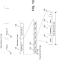
- FIG. 1B shows a schematic representation of an example TD-SCDMA data structure.
- Data is transmitted as a series of radio frames 130, 132, etc., each having a duration of 10 ms (milliseconds).
- Each radio frame is divided into two subframes 134 and 136, each having duration of 5 ms.
- Each subframe is made up of seven time slots TS0 138, TS1 150, etc., each having a duration of 0.675 ms.
- Each time slot includes four parts, a midamble 152 with one hundred and forty-four (144) chips duration, two data fields 154, 156 with three hundred and fifty-two (352) chips duration before and after the midamble 152, followed by a guard period 158 of sixteen (16) chips.
- the midamble 152 carries known data and is used by the receiver to perform channel estimation.
- the seven time slots (e.g., TS0, TS1, etc.) in each subframe (e.g., 134 or 136) may be divided between uplink and downlink traffic, according to the traffic in each direction.
- the BRP 110 may process data on a TTI basis.
- the BRP 110 may be partitioned into two main computational elements 1) BRP front end processing and 2) BRP back end processing.
- BRP front end processing consists of all processing blocks before the Hybrid Automatic Repeat ReQuest (HARQ) memory, including de-modulation, de-interleaver and de-rate matching.
- HARQ Hybrid Automatic Repeat ReQuest
- BRP 110 backend processing includes all processing blocks after the HARQ memory followed by the front end processing.
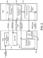
- FIG. 2 shows an example of the joint detection pre-processing module 104, the JDA 106 and the PostJD module 108 implemented in both software and hardware, and the data flow control among the software and hardware.
- software broadly refers to a collection of computer programs and procedures that perform some tasks on a computer system or a distributed computing system. Software can offer a wide variety of features with great flexibility because programming codes can be easily updated.
- hardware may refer to physical apparatus and devices, such as circuitry, microchips, digital processor, and micro-controller, etc.
- Digital signal processing hardware may offer robust and fast signal processing, but it may be more difficult to upgrade hardware to offer new functionality. By carefully partitioning an application so that some portions of the application are implemented in software and some portions of the application are implemented in hardware, a signal processing system can achieve better results than if only either software or hardware is used.
- both the JDA 106 and PostJD module 108 are implemented in hardware.
- the JDA 106 can be further partitioned into a JDA front end processor 208 and a JDA back end processor 210.
- the PostJD module 108 obtains data from the JD Back End processing module 210 and delivers physical channel de-mapped symbols to the BRP 110.
- the PostJD module 108 also provides a Signal-to-Interference-and-Noise-Ratio (SINR) estimation to a parameter estimation module 204 on the software side.
- SINR Signal-to-Interference-and-Noise-Ratio
- a channel quality indicator (CQI) estimation module 206 may also receive data from the PostJD module 108.
- the PostJD module 108 can be further partitioned between hardware for HSDPA data channels (HS-DSCH) (e.g., extracting HSDPA physical channel data) and software for all other channels.
- HSDPA data channels HS-DSCH
- the PostJD module 108 enables an added layer of flexibility on top of the existing hardware. This feature provides flexibility to support future evolution of the TD-SCDMA standard, which may require additional processing or stricter requirements for SINR and constellation gain estimation than what the current PostJD hardware is designed for.
- Radio frequency (RF) receivers e.g., the receiver 10 in FIG. 1A
- transmitters employing direct conversion architectures generate in-phase and quadrature (IQ) signals.
- IQ signals may have distortions that limit subsequent demodulator or modulator performance.
- the distortions called quadrature errors, are caused by the gain and phase imbalances between the IQ signal components. Imbalance in IQ signals may induce an image frequency and direct current offset which interfere with the demodulation or modulation process.
- a joint detection pre-processing module 104 may be used, as shown in FIG. 2 .
- the JDA front-end processor 208 receives pre-processed IQ samples, channel information and control information such as channelization codes, and produces intermediate results that are used by a JD active code detection (ACD) module 202.
- This module 202 estimates the active codes for each of the time slots after receiving output data from the JD front end processing module 208.
- the active code detection algorithm may be implemented in software.
- a JDA back-end processing module 210 is enabled after receiving the list of active codes from the software.
- an operation mode called ACD-skip may be support by the hardware-software partitioning architecture shown in FIG. 2 . That is, if a set of active codes is known in advance, the JD ACD module 202 becomes transparent.
- the design target of the receiver 10 described in this documents is to support both 384 Kbps and 2.8 Mbps channels. HSDPA channels at up to 2.8 Mbps and the 384 Kbps channels contain different sets of data.
- the data flow control for different data channels in a single hardware processor is a challenge to ensure a high performance TD-SCDMA system.
- the switching between the 384 Kbps and the 2.8 Mbps applications is implemented on the fly in the hardware processor without stalling the overall receiver system 10.
- a software programming model is used to enable handshaking between software and hardware modules at different hardware processing stages.
- the receiver 10 is capable of supporting both TD-SCDMA Release 4 and Release 5 of the 3GPP standard without hardware stalling. This is accomplished by carefully designing hardware interfaces together with a set of software programming models to implement handshake protocols between the hardware and software.
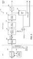
- FIG. 3 shows an implementation of HSDPA PostJD data flow control.
- An output first-in, first-out (FIFO) 302 of the JDA 106 buffers different data sets at the different processing stages.
- a top level state machine (not shown in FIG. 3 ), which can be implemented in hardware, controls the data sets that are stored in the output FIFO 302. This mechanism makes the downstream hardware processing for a HSDPA application (i.e., a cell phone, a data card) available, yet it can still support 384Kbps channels in one TTI.
- a HSDPA application i.e., a cell phone, a data card
- a HSDPA application may process data on a TTI basis, while the PostJD module 108 operates on a timeslot basis. This distinction may result in hardware stalling when HSDPA data is delivered from the FIFO 302 to the PostJD module 108, or when data is sent to the BRP 110 from the PostJD module 108.
- software control or a HSDPA programming model can be implemented to temporarily hold data processing at the beginning of the post JD processing (i.e., the PostJD module 108 operations) and the beginning of the bit rate processing (i.e., the BRP 110 operations).
- IRQs maskable interrupt requests
- a general interrupt mask register may determine which interrupts can be generated. In some examples, when an interrupt mask bit is set, it can prevent the associated interrupt from propagating out to the interrupt output of the BRP 110, but the associated interrupt status bit will still be set in the global interrupt status register. When an interrupt is active while its interrupt mask bit is cleared, the interrupt will propagate to the BRP 110 output. By default, all mask bits are set to 1, so in order to generate the required interrupts, their associated mask bits may be cleared first.
- the HSDPA programming model can define a flag that notifies the hardware which time slot contains HSDPA channel codes, thereby switching data processing from 384Kbps channels to the HSDPA applications, or vise versa, seamlessly.
- the HSDPA programming model may define the data flow such that the top level hardware state machine monitors the hardware processing stages to enable or disable data transfers from the JDA 106 to the PostJD module 108 and further to the software and the BRP 110 at the appropriate time.
- the HSDPA programming model can define the operations performed by the PostJD module 108 and the BRP 110.
- JD post processing for combined dedicated channels and the HSDPA control channels may be implemented in software.
- the output of PostJD processing for HSDPA data channels may be directly sent to the BRP module 110.
- the JD post processing may be performed in two independent ways: a software solution for non-HSDPA channels, and a PostJD hardware solution for processing of HSDPA channel codes.
- JDA input data includes input data may in a pre-defined format (e.g., a 16-bit sequence with a specific allocation for each bit).
- a PostJD hardware processor may be controlled or enabled by a particular bit in the JDA 106 input data sequence (e.g., a HSDPAenable bit in the 16-bit sequence).
- channel codes of multiple transmission rates and standards are delivered through JDA 106 output.
- a multiplexer may select and direct non-HSDPA channel codes to software for further signal processing. The selection can be done by setting a JDA_OUT_MODE bit in a PostJD Configuration Register.
- Non-HSDPA codes are extracted by performing a non-HSDPA Data Extraction algorithm (e.g., using nHSDPADatExt module 304).
- the HSDPAenable bit embedded in the JDA input may enable PostJD hardware 108 and cause HSDPA channel code to be routed to the hardware Post JD 108 after performing HSDPA data extraction calculations (i.e., after the HSDPADatExt module 306).
- Input data from the JDA output FIFO 302 contains various channel codes.
- the HSDPA Data Extraction module (HSDPADatExt) 306 extracts HSDPA data and feeds the data to the Constellation Rotation and Gain Estimation module (ConRotGain) 308.
- the ConsRotGain module 308 may rotate the constellation of the HSDPA data such that it resembles the frequency division duplex (FDD) constellation.
- FDD frequency division duplex
- the Constellation Gain Estimation 308, SINR estimation 316 and demodulation in the downstream processing as shown in FIG. 3 may subsequently all assume FDD constellation format.
- the ConsRotGain module 308 completes its calculation, if the JDA_OUT_MODE bit is set, the nHSDPADatExt module 304 is enabled to perform the data extraction for non-HSDPA channel codes. The extracted data is written back into the JDA output FIFO module 302, and the data is then sent out through the external co-processor I/F port (ECP) interface. If the JDA_OUT_MODE bit is reset, all channel codes are sent out through the ECP interface.
- the PostJD module 108 may make no assumptions about the constellation gain (i.e., channel scaling factor) and perform a "blind" constellation gain estimation.
- SINR and Constellation Gain may be both needed in BRP 110 and in software with different requirements regarding precision and reporting format.
- SINR may be calculated, for example, in 8.8 unsigned fractional format that is useful for CQI calculation in software. This value may be saved in one of the PostJD 108 output registers POST_JD_SINR_S0 to POST_JD_SINR_S4 correspondingly for each of the time slot in a single TTI, such that the software can retrieve the value at a later time.
- the constellation gain is calculated in a specific format, such as 1.12 unsigned fractional format internally, but for software purposes it is more convenient to have a different format, such that a resulting value can be reformatted to avoid saturation. For example, the least significant bits (LSBs) are first zero padded to 16-bit length and then the resulting value becomes saturated.
- LSBs least significant bits
- the SINR value needs to be reformatted into a slot-exponent.
- This value can be derived from the SINR value in many ways, where a preferred approach is to choose an appropriate bit-slice of the SINR value and use log2 of it as exponent.
- the PostJD 108 also has a number of read-only registers that are typically used for reporting its data processing status to other components in the receiver 10.
- constellation gain registers CONST_GAIN_S0 to CONST_GAIN_S4 may be used to store constellation gain obtained through hardware for each of the time slot, such that software can poll these registers anytime.
- the constellation gain can be multiplied by 2 to resolve a difference in the definition of the constellation gain in PostJD 108 and BRP 110, and quantized into the same bit width as the main output to the BRP input memory.
- the sign bit can be omitted, and the resulting output may be 7 bits wide in 0.7 unsigned fractional format.
- the expected constellation gain may be given by software, in which case the constellation gain estimation is disabled.
- a control bit i.e., ConsGainEn
- the constellation gain is supplied to the SINR estimation module 316 directly.
- One slot memory may be used to buffer the data from ConsRotGain module 308.
- the downstream PostJD computations may include the Physical Channel Demapping module 312 and SINR module 316.
- the output is supplied to the BRP 110 and the software as shown in FIG. 4 .
- the PostJD module 108 completes processing for each Time Slot and for each Frame, it sends out EOS and EOF (End Of Slot and End Of Frame) signals respectively to indicate to the BRP processor 110 that the PostJD processor 108 has completed sending the data to the BRP Frame Buffer.
- EOS and EOF interrupt requests are sent to the DSP (not shown).
- the BRP processor 110 internal control register bit i.e., the Software Ready bit, is used to trigger the BRP 110 processing.
- This offers flexibility for the software to provide its own SINR and Constellation Gain to the downstream processing, in place of values that are provided by PostJD hardware calculation. This feature permits the algorithm to be optimized from time to time largely independent of PostJD hardware.
- the BRP 110 may be configured to send the "BRP Input Ready interrupt" request to indicate to the software that the BRP 110 is ready to accept the next TTI data from PostJD 108.
- This interrupt request also initializes the next TTI data transfer to the JDA 106 hardware.
- the JDA 106 may start chip rate processing, and save all the data to the JDA 106 output FIFO 302.
- the non-HSDPA data is extracted and is written back to the same JDA Output FIFO 302 when PostJD constellation gain is determined for each time slot.
- the JDA processing is reused in both HSDPA and 384Kbps data channels.
- This feature also enables the hardware design and associated software programming model to be dedicated to the HSDPA application specification while still have the ability to process data that complies with different standards.
- the active codes may be reordered by software, so that the HS-DSCH codes are the first to be processed in the JDA 106. This prevents a change in the number of non-HSDPA UE codes in use between two time slots which will affect the relative positioning of the HS-DSCH channels, thereby allowing these channels to be programmed only once per TTI.
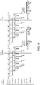
- FIG. 4 shows data transfer in the HSDPA receiver 10 in a series of nine consecutive time slots with reference to the system configuration in FIG. 1A . More specifically, the table in FIG. 5 summarizes the major data transferring occurred during each time slot. For example, referring to rows 1, 3, 8 and 9 in FIG. 5 , the HSDPA receiver 10 may rely on data calculated and supplied by the software. Row 1 shows that the JDA 106 implemented as the first component in the HSDAP signal chain operates once per downlink time slot. The JDA 106 inputs such as data samples, channelization codes, channel estimate and control information, are provided by the software and sent to the JDA hardware as one complete data transfer. The JDA 106 also produces output once per time slot.
- the second component in the HSDPA signal chain may be the PostJD module 108.
- the input data of the PostJD module 108 is obtained from the JDA 106 (i.e., time slot 4 in FIG. 4 and row 4 in FIG. 5 ) and the control parameters come from the software (i.e., time slot 8 in FIG. 4 and row 8 in FIG. 5 ).
- Post JD module 108 hardware may be programmed by the software, before the first slot of data reaches the post JD.
- the PostJD 108 programming is implemented on a TTI basis and PostJD processes data in a slot-by-slot manner.
- the PostJD module 108 output is transferred to the BRP 110 input memory in a slot-by-slot manner and this transfer is handled internally by the hardware. That is, data is usually downloaded in increments of one timeslot or subframe, but internally processed by the BRP 110 at the frame rate and TTI rate.
- the extracted transport blocks may be stored in the transport block buffer at the TTI rate of the associated transport channel. Transport channel data for multiple transport channels with the same TTI will become available at the same time.
- the frame rate operation in BRP 110 requires downloading frame data and frame configuration every 10 ms.
- the TTI rate operation requires programming transport channel control registers every TTI for each active transport channel. BRP 110 programming is thus implemented on a TTI basis, and BRP 110 co-processor produces output once every HSDPA TTI.
- FIG. 6 lists interrupts and recommended software actions.
- BRP110 will raise interrupt HS_BRP_DONE upon completing the processing of a current TTI such that the software can program BRP 110 parameters for the next TTI.
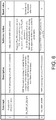
- FIG. 7 summarizes the parameters that control the intended execution sequence for HSDPA and non-HSDPA processing with regards to the HSDPA processing chain. It can be seen from the leftmost column of the table in FIG. 7 that when the receiver 10 is not processing HSDPA data, the register HS_RX_EN bit may be set to zero. In this case, the JDA 106 may work independently of the PostJD module 108 and the BRP 110 accordingly disables HSDPA processing.
- the register HS_RX_EN bit can be set to 1 to enable HSDPA processing. This also informs the JDA 106 to act on the HSDPA enable bit and activate the PostJD module 108 for time slots containing HSDPA data and ultimately triggers the BRP 110 when the entire TTI is received.
- the JDA 106 Since not all timeslots in a HSDPA TTI contain HSDPA data, the JDA 106 is informed via the HSDPA enable bit which time slots to process as HSDPA timeslots and which to treat as if the HS_RX_EN bit is 0. When HSDPA enable bit is 0, the JDA 106 may not exchange data or signal the PostJD module108, but rather sends out all output data via direct memory access (DMA) after completing execution. When HSDPA enable bit is 1, the PostJD module 108 is triggered upon JDA 106 completion.
- DMA direct memory access
- the PostJD module 108 may indicate to the software that the configuration of the PostJD module 108 has not been performed, and the PostJD module 108 also stalls until the configuration is successfully written and a CONFIG_READY bit is set to 1.
- PostJD module 108 then copies the HSDPA data from the JDA output buffer and signals the JDA 106.
- the JD_OUTPUT_MODE bit is from PostJD module 108 configuration register.
- the JD_OUTPUT_MODE bit is programmed per TTI, so even though it only affects the JDA 106 it is programmed with the PostJD module 108 on a TTI basis.
- the PostJD module 108 may keep count of the number of HSDPA timeslots in the TTI based on HS_RX_TSs bitand the number of times it is triggered by JDA 106. Once the PostJD module 108 determines that the whole TTI has been received it triggers the BRP 110.
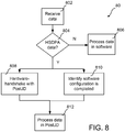
- FIG. 8 is a flow diagram showing an example process 80 for controlling data flow in the receiver 10.
- input data are received (802) by the JD pre-processing module 104, and as shown in FIG. 2 , data will be further processed by the JDA front end processor 106.
- HSDPA channel data can be extracted and a signal may be sent 804 to the PostJD module 108 according to the hardware handshake protocol between the JDA 106 and the PostJD module 108 to indicate that the data is ready for downstream processing.
- the receiver 10 may identify 806 whether software configuration of the PostJD module 108 is completed or not. If both conditions are satisfied, the PostJD module 108 starts processing 808 data.
- the SINR and constellation gain output registers can be accessed on a slot-by-slot basis if desired, but can also be read out after the completion of the TTI.
- the SINR output ready (which may be used for CQI calculation) is signaled by a time slot completion interrupt for each time slot.
- PostJD module 108 includes a status register comprising a number of status bits that can be used to check the progress of the hardware of the PostJD module 108.
- bits EOS0 to EOS4 in the status register are dedicated for saving the status for each time slot in a TTI.
- the software can mask out any undesired slot completion interrupt.
- the hardware needs to be flexible enough to allow any or all of these interrupts to be processed by software.
- the numbering of the slot completion interrupts is relative. For example, if three time slots are in use, the last slot in a frame may correspond to EOS2, regardless of which physical timeslot is used.
- the software may also apply BRP flow control by delaying the programming of the BRP 110. This operation halts the signal chain upon PostJD completion (When EOF is issued) and allows software to manipulate the constellation gain and SINR for each slot within the frame before triggering the BRP 110. The processing is resumed by writing the BRP configuration register.
- the SINR and Constellation Gain parameters may be accessed through a BRP debug interface (not shown).
- connections may be wired or wireless connections.
- the module may be directly connected or indirectly connected (via, e.g., still another module) to the other module.
- the methods and systems described herein may be implemented on many different types of processing devices by program code comprising program instructions that are executable by one or more processors.
- the software program instructions may include source code, object code, machine code, or any other stored data that is operable to cause a processing system to perform methods described herein.
- the systems and methods may be provided on many different types of computer-readable media including computer storage mechanisms (e.g., CD-ROM, diskette, RAM, flash memory, computer's hard drive, etc.) that contain instructions for use in execution by a processor to perform the methods' operations and implement the systems described herein.
- computer storage mechanisms e.g., CD-ROM, diskette, RAM, flash memory, computer's hard drive, etc.
- the computer components, software modules, functions and data structures described herein may be connected directly or indirectly to each other in order to allow the flow of data needed for their operations. It is also noted that software instructions or a module can be implemented for example as a subroutine unit of code, or as a software function unit of code, or as an object (as in an object-oriented paradigm), or as an applet, or in a computer script language, or as another type of computer code or firmware.
- the software components and/or functionality may be located on a single device or distributed across multiple devices depending upon the situation at hand.
Landscapes
- Engineering & Computer Science (AREA)
- Computer Networks & Wireless Communication (AREA)
- Signal Processing (AREA)
- Mobile Radio Communication Systems (AREA)
Claims (14)
- Verfahren zum Steuern eines Datenflusses in einem System zur drahtlosen Kommunikation, aufweisend:Empfangen von Daten in einem ersten Datenverarbeitungsmodul, wobei das erste Datenverarbeitungsmodul einen in Hardware implementierten Beschleuniger für gemeinsame Erkennung (106; 208, 210) aufweist;Freigeben eines zweiten Datenverarbeitungsmoduls, wenn mindestens ein Signalzeitfenster der empfangenen Daten Daten aufweist, welche einen ersten Datenübertragungsstandard erfüllen, wobei das zweite Datenverarbeitungsmodul ein in Hardware implementiertes Nachbearbeitungsmodul für gemeinsame Erkennung (108) aufweist;Austauschen von Signalen zwischen dem ersten Datenverarbeitungsmodul und einem Prozessor, der eine Software ausführt, um anzuzeigen, dass das erste Datenverarbeitungsmodul bereit ist, Daten an das zweite Datenverarbeitungsmodul zu übertragen, und zu bestimmen, dass eine erste Software-Konfiguration des zweiten Datenverarbeitungsmoduls abgeschlossen ist;Verarbeiten der Daten in dem zweiten Datenverarbeitungsmodul für das mindestens eine Zeitfenster; undFreigeben eines dritten Datenverarbeitungsmoduls (110) bei einer Vollendung einer Verarbeitung von mindestens einem Datenblock in dem zweiten Datenverarbeitungsmodul, Bestimmen, dass eine zweite Software-Konfiguration des dritten Datenverarbeitungsmoduls abgeschlossen ist, und Verarbeiten des mindestens einen Datenblocks, wobei der mindestens eine Datenblock mehrere Zeitfenster umfasst.
- Verfahren gemäß Anspruch 1, wobei der Beschleuniger für gemeinsame Erkennung (106; 208, 210) ein erstes First-In-First-Out- (FIFO-) Modul aufweist.
- Verfahren gemäß Anspruch 1 oder 2, wobei das erste Datenverarbeitungsmodul (106; 208, 210) eingerichtet ist zum:Extrahieren von Daten, die einen zweiten Datenübertragungsstandard erfüllen, und Verarbeiten der Daten in dem zweiten Datenübertragungsstandard durch den Prozessor, der eine Software ausführt.
- Verfahren gemäß einem der Ansprüche 1 bis 3, wobei das dritte Datenverarbeitungsmodul einen Bitratenprozessor (110) aufweist.
- Verfahren gemäß einem der Ansprüche 1 bis 4 wobei der Prozessor der eine Software ausführt, einen Konstellations-Verstärkungswert an das zweite Datenverarbeitungsmodul (108) bereitstellt.
- Verfahren gemäß einem der Ansprüche 1 bis 5, wobei das zweite Datenverarbeitungsmodul (108) eingerichtet ist, einen Signal-zu-Störungs-und-Rausch-Verhältnis- (SINR-) Wert auf einer Zeitfensterbasis bereitzustellen, wobei der SINR-Wert optional auf einer Zeitfensterbasis berechnet wird.
- Vorrichtung zum Steuern eines Datenflusses in einem System zur drahtlosen Kommunikation, aufweisend:ein erstes Datenverarbeitungsmodul, das Daten empfängt, wobei das erste Datenverarbeitungsmodul einen in Hardware implementierten Beschleuniger für gemeinsame Erkennung (106; 208, 210) aufweist;eine Schaltung zum Anzeigen, dass das erste Datenverarbeitungsmodul bereit ist, die Daten zu einem zweiten Datenverarbeitungsmodul (108) zu übertragen, und zum Bestimmen, dass eine Software-Konfiguration des zweiten Datenverarbeitungsmoduls abgeschlossen ist, wobei das zweite Datenverarbeitungsmodul mindestens ein Signalzeitfenster extrahiert und verarbeitet, welches Daten aufweist, die einen ersten Datenübertragungsstandard erfüllen, wobei das zweite Datenverarbeitungsmodul ein in Hardware implementiertes Nachverarbeitungsmodul für gemeinsame Erkennung (108) aufweist; undein drittes Datenverarbeitungsmodul (110), das angepasst ist, bei einer Vollendung eines Verarbeitens von mindestens einem Datenblock in dem zweiten Datenverarbeitungsmodul freigeschaltet zu werden, und den mindestens einen Datenblock zu verarbeiten, wobei der mindestens eine Datenblock mehrere Signalzeitfenster umfasst.
- Vorrichtung gemäß Anspruch 7, wobei das erste Datenverarbeitungsmodul (106; 208, 210) eingerichtet ist zum:Extrahieren von Daten, die einen zweiten Datenübertragungsstandard erfüllen, und Verarbeiten der Daten in dem zweiten Datenübertragungsstandard durch einen Prozessor, der eine Software ausführt.
- Vorrichtung gemäß Anspruch 7 oder 8, wobei das zweite Datenverarbeitungsmodul (108) Ausgangsdaten von dem ersten Datenverarbeitungsmodul (106; 208, 210) verarbeitet und in ein Format konvertiert, das für das dritte Datenverarbeitungsmodul (110) geeignet ist.
- Vorrichtung gemäß einem der Ansprüche 7 bis 9, wobei das dritte Datenverarbeitungsmodul einen Bitratenprozessor (110) aufweist.
- Vorrichtung gemäß einem der Ansprüche 8 bis 10, wobei der Prozessor, der eine Software ausführt, einen Konstellations-Verstärkungswert an das zweite Datenverarbeitungsmodul (106; 208, 210) bereitstellt.
- Vorrichtung gemäß einem der Ansprüche 7 bis 11, wobei das zweite Datenverarbeitungsmodul (106; 208, 210) eingerichtet ist, einen Signal-zu-Störungs-und-Rausch-Verhältnis- (SINR-) Wert bereitzustellen, wobei der SINR-Wert optional auf einer Zeitfensterbasis berechnet wird.
- Vorrichtung gemäß einem der Ansprüche 7 bis 12, wobei der erste Datenübertragungsstandard Highspeed-Downlink-Packet-Access (HSDPA) einschließt.
- Verfahren gemäß einem der Ansprüche 1 bis 6, wobei der erste Datenübertragungsstandard Highspeed-Downlink-Packet-Access (HSDPA) einschließt.
Applications Claiming Priority (3)
| Application Number | Priority Date | Filing Date | Title |
|---|---|---|---|
| US896607P | 2007-12-21 | 2007-12-21 | |
| US9326908P | 2008-08-29 | 2008-08-29 | |
| US12/254,201 US8316378B2 (en) | 2007-12-21 | 2008-10-20 | Data flow control in wireless communication systems |
Publications (2)
| Publication Number | Publication Date |
|---|---|
| EP2073397A1 EP2073397A1 (de) | 2009-06-24 |
| EP2073397B1 true EP2073397B1 (de) | 2017-02-15 |
Family
ID=40513937
Family Applications (1)
| Application Number | Title | Priority Date | Filing Date |
|---|---|---|---|
| EP08171811.6A Ceased EP2073397B1 (de) | 2007-12-21 | 2008-12-16 | Datenflusssteuerung in Hochgeschwindigkeits-Abwärtsstrecken-Paketzugang (HSDPA) |
Country Status (3)
| Country | Link |
|---|---|
| US (1) | US8316378B2 (de) |
| EP (1) | EP2073397B1 (de) |
| TW (1) | TWI400893B (de) |
Families Citing this family (7)
| Publication number | Priority date | Publication date | Assignee | Title |
|---|---|---|---|---|
| US20100103983A1 (en) * | 2008-10-29 | 2010-04-29 | Yi-Pin Wang | Root spreading code based assignment for hsdpa |
| CN102439516B (zh) | 2010-01-20 | 2013-01-23 | 深圳超多维光电子有限公司 | 扭曲向列液晶盒及包含该液晶盒的2d-3d立体显示装置 |
| US8483156B2 (en) | 2010-05-03 | 2013-07-09 | Nokia Siemens Networks Oy | Feedback for inter-radio access technology carrier aggregation |
| US8498666B2 (en) | 2010-05-05 | 2013-07-30 | Nokia Siemens Networks Oy | Carrier aggregation for two radio systems |
| US8837358B2 (en) | 2010-10-18 | 2014-09-16 | Nokia Siemens Networks Oy | UL ACK/NACK for inter-radio access technology carrier aggregation |
| CN110929857B (zh) * | 2018-09-20 | 2023-04-18 | 合肥君正科技有限公司 | 一种神经网络的数据处理方法和装置 |
| CN114116557B (zh) * | 2021-11-15 | 2024-02-27 | 同济大学 | 基于硬件加速器与数字信号处理器的信道估计装置及方法 |
Family Cites Families (15)
| Publication number | Priority date | Publication date | Assignee | Title |
|---|---|---|---|---|
| US896608A (en) | 1906-06-15 | 1908-08-18 | Vulkan Maschinenfabriks Actien Ges | Arrangement of the winding of electromagnetic clutches. |
| US4893234A (en) * | 1987-01-15 | 1990-01-09 | United States Department Of Energy | Multi-processor including data flow accelerator module |
| US5235594A (en) * | 1991-08-09 | 1993-08-10 | Westinghouse Electric Corp. | Time division multiplex voice data bus |
| JP3323124B2 (ja) | 1998-01-09 | 2002-09-09 | 富士通株式会社 | 変調方法及び装置 |
| US7110431B2 (en) | 2001-03-14 | 2006-09-19 | Mercury Computer Systems, Inc. | Hardware and software for performing computations in a short-code spread-spectrum communications system |
| CN100576772C (zh) * | 2002-12-27 | 2009-12-30 | Nxp股份有限公司 | 具有智能天线的移动终端及其方法 |
| US7269207B2 (en) * | 2003-02-05 | 2007-09-11 | Nokia Corporation | Method of symbol index selection in code division multiple access |
| US7756483B2 (en) * | 2003-06-16 | 2010-07-13 | Broadcom Corporation | Adaptive channel quality estimation algorithm to support link adaptation |
| EP1779553A4 (de) | 2004-07-26 | 2008-02-20 | Interdigital Tech Corp | Coprozessor für hochgeschwindigkeitspaketzugriff in abwärtsverbindungen zur leistungsverbesserung eines vorhandenen modem-host |
| JP4706871B2 (ja) | 2005-03-02 | 2011-06-22 | 日本電気株式会社 | ダイバーシティ受信装置及びその利得調整方法 |
| US20070191007A1 (en) * | 2006-02-14 | 2007-08-16 | Claude Hayek | Method and system for a processor that handles a plurality of wireless access communication protocols |
| US7953958B2 (en) | 2006-09-29 | 2011-05-31 | Mediatek Inc. | Architecture for joint detection hardware accelerator |
| US7945258B2 (en) * | 2007-07-31 | 2011-05-17 | Broadcom Corporation | Wireless device operable to manipulate high-speed shared control channel (HSSCCH) quality control through channel quality indication report manipulation |
| US8155241B2 (en) | 2007-12-21 | 2012-04-10 | Mediatek Inc. | System for processing common gain values |
| US9326908B2 (en) | 2013-04-17 | 2016-05-03 | William Scott | Body stretching assembly |
-
2008
- 2008-10-20 US US12/254,201 patent/US8316378B2/en active Active
- 2008-12-16 EP EP08171811.6A patent/EP2073397B1/de not_active Ceased
- 2008-12-19 TW TW097149615A patent/TWI400893B/zh not_active IP Right Cessation
Non-Patent Citations (1)
| Title |
|---|
| None * |
Also Published As
| Publication number | Publication date |
|---|---|
| TWI400893B (zh) | 2013-07-01 |
| US20090165019A1 (en) | 2009-06-25 |
| EP2073397A1 (de) | 2009-06-24 |
| TW200929914A (en) | 2009-07-01 |
| US8316378B2 (en) | 2012-11-20 |
Similar Documents
| Publication | Publication Date | Title |
|---|---|---|
| EP2073397B1 (de) | Datenflusssteuerung in Hochgeschwindigkeits-Abwärtsstrecken-Paketzugang (HSDPA) | |
| CN101630994B (zh) | 控制数据流的方法及装置 | |
| CN101273551B (zh) | 用于传输数据的设备和方法以及用于接收数据的设备和方法 | |
| US8149702B2 (en) | Multi-mode bit rate processor | |
| EP2226949A1 (de) | Kanalschätzung für drahtlose Kommunikation | |
| US20060039330A1 (en) | High speed downlink packet access co-processor for upgrading the capabilities of an existing modem host | |
| JP5312040B2 (ja) | スペクトル拡散受信機において使用されるオンデマンド逆拡散処理 | |
| CN101917366A (zh) | 移动通信终端和控制多径干扰去除装置的起动的方法 | |
| EP2486685A1 (de) | Vorrichtung und verfahren für harq-feedback in einem drahtlosen mehrträger-kommunikationssystem | |
| US20120272042A1 (en) | Distributed micro instructions set processor architecture for high-efficiency signal processing | |
| EP2073418A2 (de) | Rundfunkrahmenverzerrung für TD-SCDMA-Systeme | |
| CN113545150A (zh) | 一种配置信息的指示方法及装置 | |
| EP3493636A1 (de) | Datenübertragungsverfahren, endgerätevorrichtung und netzwerkvorrichtung | |
| CN101540744A (zh) | 数据接收处理方法、装置与用户终端 | |
| US7023902B2 (en) | Apparatus and method for scalable offline CDMA demodulation | |
| CN101278490A (zh) | 用于多径信号分量合并的方法和设备 | |
| US8149936B2 (en) | Apparatus and methods for tile and assignment processing | |
| JP3802025B2 (ja) | 移動通信システムの初期同期検索装置及びその方法 | |
| CN101056122B (zh) | 一种宽带码分多址系统中导频的rake接收实现方法及装置 | |
| JP2004072418A (ja) | 遅延プロファイル作成方法および遅延プロファイル作成装置 | |
| CN100479340C (zh) | 一种wcdma基站的上行基带解调方法及装置 | |
| JP2005094757A (ja) | 携帯端末機の送信dcオフセット除去方法 | |
| CN101110605B (zh) | 一种发射功率控制数据的瑞克接收装置及方法 | |
| CN101401319B (zh) | 基于宽带码分多址系统的rake接收装置及方法 | |
| KR101593422B1 (ko) | Pci 시그널링 설계를 위한 방법 및 장치 |
Legal Events
| Date | Code | Title | Description |
|---|---|---|---|
| PUAI | Public reference made under article 153(3) epc to a published international application that has entered the european phase |
Free format text: ORIGINAL CODE: 0009012 |
|
| AK | Designated contracting states |
Kind code of ref document: A1 Designated state(s): AT BE BG CH CY CZ DE DK EE ES FI FR GB GR HR HU IE IS IT LI LT LU LV MC MT NL NO PL PT RO SE SI SK TR |
|
| AX | Request for extension of the european patent |
Extension state: AL BA MK RS |
|
| 17P | Request for examination filed |
Effective date: 20091118 |
|
| 17Q | First examination report despatched |
Effective date: 20091214 |
|
| AKX | Designation fees paid |
Designated state(s): DE FR GB |
|
| REG | Reference to a national code |
Ref country code: DE Ref legal event code: R079 Ref document number: 602008048749 Country of ref document: DE Free format text: PREVIOUS MAIN CLASS: H04B0001707000 Ipc: H04B0001710500 |
|
| GRAP | Despatch of communication of intention to grant a patent |
Free format text: ORIGINAL CODE: EPIDOSNIGR1 |
|
| RIC1 | Information provided on ipc code assigned before grant |
Ipc: H04J 13/00 20110101ALI20160620BHEP Ipc: H04B 1/7105 20110101AFI20160620BHEP |
|
| INTG | Intention to grant announced |
Effective date: 20160712 |
|
| GRAS | Grant fee paid |
Free format text: ORIGINAL CODE: EPIDOSNIGR3 |
|
| GRAA | (expected) grant |
Free format text: ORIGINAL CODE: 0009210 |
|
| AK | Designated contracting states |
Kind code of ref document: B1 Designated state(s): DE FR GB |
|
| REG | Reference to a national code |
Ref country code: GB Ref legal event code: FG4D |
|
| REG | Reference to a national code |
Ref country code: DE Ref legal event code: R096 Ref document number: 602008048749 Country of ref document: DE |
|
| REG | Reference to a national code |
Ref country code: DE Ref legal event code: R097 Ref document number: 602008048749 Country of ref document: DE |
|
| PLBE | No opposition filed within time limit |
Free format text: ORIGINAL CODE: 0009261 |
|
| STAA | Information on the status of an ep patent application or granted ep patent |
Free format text: STATUS: NO OPPOSITION FILED WITHIN TIME LIMIT |
|
| REG | Reference to a national code |
Ref country code: FR Ref legal event code: PLFP Year of fee payment: 10 |
|
| 26N | No opposition filed |
Effective date: 20171116 |
|
| P01 | Opt-out of the competence of the unified patent court (upc) registered |
Effective date: 20230607 |
|
| PGFP | Annual fee paid to national office [announced via postgrant information from national office to epo] |
Ref country code: GB Payment date: 20231227 Year of fee payment: 16 |
|
| PGFP | Annual fee paid to national office [announced via postgrant information from national office to epo] |
Ref country code: FR Payment date: 20231227 Year of fee payment: 16 |
|
| PGFP | Annual fee paid to national office [announced via postgrant information from national office to epo] |
Ref country code: DE Payment date: 20231229 Year of fee payment: 16 |
|
| REG | Reference to a national code |
Ref country code: DE Ref legal event code: R119 Ref document number: 602008048749 Country of ref document: DE |
|
| GBPC | Gb: european patent ceased through non-payment of renewal fee |
Effective date: 20241216 |
|
| PG25 | Lapsed in a contracting state [announced via postgrant information from national office to epo] |
Ref country code: DE Free format text: LAPSE BECAUSE OF NON-PAYMENT OF DUE FEES Effective date: 20250701 |
|
| PG25 | Lapsed in a contracting state [announced via postgrant information from national office to epo] |
Ref country code: GB Free format text: LAPSE BECAUSE OF NON-PAYMENT OF DUE FEES Effective date: 20241216 |
|
| PG25 | Lapsed in a contracting state [announced via postgrant information from national office to epo] |
Ref country code: FR Free format text: LAPSE BECAUSE OF NON-PAYMENT OF DUE FEES Effective date: 20241231 |