EP2074560B1 - Procédé de fabrication pour un insert transpondeur pour un document personnel - Google Patents
Procédé de fabrication pour un insert transpondeur pour un document personnel Download PDFInfo
- Publication number
- EP2074560B1 EP2074560B1 EP08785744A EP08785744A EP2074560B1 EP 2074560 B1 EP2074560 B1 EP 2074560B1 EP 08785744 A EP08785744 A EP 08785744A EP 08785744 A EP08785744 A EP 08785744A EP 2074560 B1 EP2074560 B1 EP 2074560B1
- Authority
- EP
- European Patent Office
- Prior art keywords
- substrate layer
- transponder
- chip module
- window opening
- chip
- Prior art date
- Legal status (The legal status is an assumption and is not a legal conclusion. Google has not performed a legal analysis and makes no representation as to the accuracy of the status listed.)
- Not-in-force
Links
Images
Classifications
-
- G—PHYSICS
- G06—COMPUTING OR CALCULATING; COUNTING
- G06K—GRAPHICAL DATA READING; PRESENTATION OF DATA; RECORD CARRIERS; HANDLING RECORD CARRIERS
- G06K19/00—Record carriers for use with machines and with at least a part designed to carry digital markings
- G06K19/06—Record carriers for use with machines and with at least a part designed to carry digital markings characterised by the kind of the digital marking, e.g. shape, nature, code
- G06K19/067—Record carriers with conductive marks, printed circuits or semiconductor circuit elements, e.g. credit or identity cards also with resonating or responding marks without active components
- G06K19/07—Record carriers with conductive marks, printed circuits or semiconductor circuit elements, e.g. credit or identity cards also with resonating or responding marks without active components with integrated circuit chips
- G06K19/077—Constructional details, e.g. mounting of circuits in the carrier
-
- G—PHYSICS
- G06—COMPUTING OR CALCULATING; COUNTING
- G06K—GRAPHICAL DATA READING; PRESENTATION OF DATA; RECORD CARRIERS; HANDLING RECORD CARRIERS
- G06K19/00—Record carriers for use with machines and with at least a part designed to carry digital markings
- G06K19/06—Record carriers for use with machines and with at least a part designed to carry digital markings characterised by the kind of the digital marking, e.g. shape, nature, code
- G06K19/067—Record carriers with conductive marks, printed circuits or semiconductor circuit elements, e.g. credit or identity cards also with resonating or responding marks without active components
- G06K19/07—Record carriers with conductive marks, printed circuits or semiconductor circuit elements, e.g. credit or identity cards also with resonating or responding marks without active components with integrated circuit chips
- G06K19/077—Constructional details, e.g. mounting of circuits in the carrier
- G06K19/07749—Constructional details, e.g. mounting of circuits in the carrier the record carrier being capable of non-contact communication, e.g. constructional details of the antenna of a non-contact smart card
-
- G—PHYSICS
- G06—COMPUTING OR CALCULATING; COUNTING
- G06K—GRAPHICAL DATA READING; PRESENTATION OF DATA; RECORD CARRIERS; HANDLING RECORD CARRIERS
- G06K19/00—Record carriers for use with machines and with at least a part designed to carry digital markings
- G06K19/02—Record carriers for use with machines and with at least a part designed to carry digital markings characterised by the selection of materials, e.g. to avoid wear during transport through the machine
- G06K19/025—Record carriers for use with machines and with at least a part designed to carry digital markings characterised by the selection of materials, e.g. to avoid wear during transport through the machine the material being flexible or adapted for folding, e.g. paper or paper-like materials used in luggage labels, identification tags, forms or identification documents carrying RFIDs
-
- G—PHYSICS
- G06—COMPUTING OR CALCULATING; COUNTING
- G06K—GRAPHICAL DATA READING; PRESENTATION OF DATA; RECORD CARRIERS; HANDLING RECORD CARRIERS
- G06K19/00—Record carriers for use with machines and with at least a part designed to carry digital markings
- G06K19/06—Record carriers for use with machines and with at least a part designed to carry digital markings characterised by the kind of the digital marking, e.g. shape, nature, code
- G06K19/067—Record carriers with conductive marks, printed circuits or semiconductor circuit elements, e.g. credit or identity cards also with resonating or responding marks without active components
- G06K19/07—Record carriers with conductive marks, printed circuits or semiconductor circuit elements, e.g. credit or identity cards also with resonating or responding marks without active components with integrated circuit chips
- G06K19/077—Constructional details, e.g. mounting of circuits in the carrier
- G06K19/07745—Mounting details of integrated circuit chips
-
- Y—GENERAL TAGGING OF NEW TECHNOLOGICAL DEVELOPMENTS; GENERAL TAGGING OF CROSS-SECTIONAL TECHNOLOGIES SPANNING OVER SEVERAL SECTIONS OF THE IPC; TECHNICAL SUBJECTS COVERED BY FORMER USPC CROSS-REFERENCE ART COLLECTIONS [XRACs] AND DIGESTS
- Y10—TECHNICAL SUBJECTS COVERED BY FORMER USPC
- Y10T—TECHNICAL SUBJECTS COVERED BY FORMER US CLASSIFICATION
- Y10T29/00—Metal working
- Y10T29/49—Method of mechanical manufacture
- Y10T29/49002—Electrical device making
- Y10T29/49016—Antenna or wave energy "plumbing" making
Definitions
- the present invention relates to a method for producing a transponder inlay according to the preamble of claim 1.
- transponders which enable a non-contact, automated reading of the data stored on a chip of the transponder.
- Such transponders comprise, in addition to the chip, an antenna coil which enables non-contact data access.
- transponder inlays which have on a substrate layer, the transponder unit.
- the implementation of such a transponder inlay in a passport document would be considered as desirable as little as possible in limiting the known format of the passport documents.
- the handling of the passport documents ie, for example, the scrolling in such documents, be influenced as little as possible.
- the handling of the passport documents results in particular mechanical stresses for the transponder inlays or for the transponder units arranged on the substrate layers of the transponder inlays.
- the opening for receiving a chip module is produced either by pressing the chip module into the plastic substrate or by previously forming a suitable opening by using a pressure and temperature acting on the substrate device.
- the US 4,625,102 shows a method for arranging a chip module in a plastic substrate, in which the chip module is pressed into the plastic substrate.
- a window opening provided with an edge offset comes about in that a passage opening designed as a window opening has already been introduced into the plastic substrate, ie before the chip module has been pressed into the plastic substrate.
- the WO 88/08171 discloses a method in which a plastic substrate is provided with a recess for receiving a chip module, wherein for the preparation of the recording, a heatable stamping tool is used, which is designed as a negative of the recording.
- the stamping tool is pressed under the action of pressure and temperature in the plastic material, which is heated to the flow temperature before pressing, so that then takes place as a result of the pressurization of the plastic material to form the recording, a displacement of the plastic material according to the penetrating into the plastic material tool volume.
- the DE 4241482 A1 shows a method for producing a transponder card, in which a stamping tool is used for forming an edge-offset window opening. Even before using the stamping tool, a blind hole is introduced into the plastic material by means of a milling cutter. This blind hole is dimensioned so that it allows the inclusion of a displaced in the production of Randabsatzes by the action of the stamping tool material.
- the present invention is therefore based on the object to propose a method for producing a transponder inlays that allows the production of transponder inlays designed as thin as possible with a comparatively low outlay.
- a passage opening in the substrate layer is produced to form a window opening receiving the chip module, and the peripheral edge of the passage opening is subjected to pressure and temperature in order to achieve a compressed edge offset of reduced thickness.
- the application of pressure and temperature takes place by means of an ultrasonically excited punching tool.
- the temperature can be applied by an external heating of the stamping tool, or by an induced by the mechanical friction due to the ultrasonic vibrations of the punch tool heating of the punch tool or the substrate layer, ie without external overheating.
- the punch tool is used at the same time for the formation of the through hole, since thus both the formation of the window opening and the formation of the edge paragraph can be done in a machining operation with one and the same tool.
- a variant of the method which is optimized with regard to the universal tool insert becomes possible when the stamp tool simultaneously serves for embedding a wire conductor used for producing the antenna coil into the contact surface of the substrate layer.
- transponder inlays A preferred embodiment of the transponder inlays will be clarified with an explanation of the process steps associated with the production of the transponder inlays with reference to the drawing.
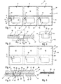
- Fig. 1 shows in a utility device 10 three interconnected trained Transponderinlays 11, each having a substrate layer 12 having arranged thereon, an antenna coil 13 and a chip module 14 comprising transponder unit 15.
- Fig. 1 beyond separating lines 16 are shown, along which a separation of the transponder inlays 11 can be made from the utility arrangement.
- Fig. 1 shows the transponder inlays 11 in a plan view with an upwardly facing contact surface 17, on the, as well as in Fig. 2 represented, a wire conductor 18 is arranged coil-shaped and embedded in the contact surface 17.
- Fig. 5 shows, free wire conductor ends 19, 20 with contact surfaces 21, 22 of a arranged in the contact surface 17 of the substrate layer 12 chip carrier 23 of the chip module 14 contacted.
- the chip module 14 is located in one of the FIGS. 2 and 3
- the window opening 30 is in the FIGS. 2 and 3 deviating from the illustration in Fig. 1 omitted inserted into the window opening 30 chip module 14.
- the window opening 30 is stepped and has a contact surface 17 facing edge shoulder 24 which serves to receive the chip carrier 23 ( Fig. 5 ) and, like Fig. 3 shows, a receiving cross-section 25 which is formed larger than a receiving cross-section 26 of a to an underside 27 of the substrate layer 12 toward extending through hole 28 which serves to receive a chip housing 29 of the chip module 14 ( Fig. 5 ).
- the chip module 14 used in the present exemplary embodiment is a chip module 14 with a chip carrier 23 which is designed to be larger than the chip housing 29 in only one dimension. Therefore, in the exemplary embodiment illustrated here, the edge shoulder 24 is designed such that the edge shoulder 24 only at two opposite edge portions support surfaces 51, 52 forms for the chip carrier 23 ( Fig. 3 ).
- a stamping tool 31 can be used which has a stamp tip 33 bounded by a stamp collar 32.
- the punch tip 33 has one of the passage opening 28 corresponding Cross section and the punch collar 32 has a cross section corresponding to the edge shoulder 24.
- the stamp tip 33 is provided at the edge of its end face 34 with a circumferentially formed cutting edge 35.
- the punch tool 31 can be moved with an intermediate arrangement of the substrate layer 12 against a support surface 53, so that substantially based on a punching process, the through hole 28 is generated by the action of the cutting edge 35 on the substrate layer 12.
- this feed movement 36 can be acted upon by ultrasonic vibrations in the direction of the feed movement or transversely thereto, so that relative heating of the substrate layer 12 takes place by the relative movement between the punch collar 32 and the contact surface 17 of the substrate layer 12.
- this heating the compression of the substrate layer 12 by the advancing movement 36 is irreversibly, ie virtually frozen.
- the material selected for the substrate layer 12 is a thermoelastic material, despite the thermal stress of the material, a certain elasticity is maintained in the compressed region of the peripheral shoulder 24. In principle, however, it is also possible to have a window opening in the in FIGS. 2 and 3 to produce shown type in a thermoplastic material.
- transponder inlays 11 of the utility device 10 are double-sided with a transponder page 37, on the each of the transponder unit 15 is located, and with a blank page 39, which is divided by a Falzaus originallyung of the transponder side 37 and coextensive with the transponder side 37 of the substrate layer 12.
- a layer structure 40 is illustrated with cover pages 49 formed integrally with one another in a utility arrangement 41.
- the utility arrangement 41 consists of the in Fig. 1 illustrated utility assembly 10 with the transponder inlays 11 and arranged on the contact surface 17 utility device 54 with composite cover layers 42nd Fig. 5 shows in a partial sectional view of the layer structure 40 of the utility assembly 41 and a cover page formed therein 49 in an enlarged view.
- the chip module 14 is arranged in the window opening 30 of the substrate layer 12 such that a contact side 43 of the chip carrier 23 is substantially flush with the contact surface 17 of the substrate layer 12.
- a housing upper side 45 is in this case set back slightly inward into the window opening 30 or arranged substantially flush with an underside 46 of the substrate layer 12.
- the chip carrier 23 is bonded to the support surfaces 51, 52 of the edge shoulder 24.
- Fig. 5 further shows that between the cover layer 42 and the contact surface 17 of the substrate layer 12 and the transponder inlays 11, an adhesive intermediate layer 47 connecting the cover layer 42 and the transponder inlay 11 to a fixed layer structure 40 is arranged.
- the contacted with the contact surfaces 21, 22 of the chip carrier 23 wire conductor ends 19, 20 of the antenna coil 13 are accommodated to a substantial extent in the intermediate layer 47, so that even with an inelastic formation of the cover layer 42 an image of the wire conductor ends 19, 20 in an outer or visible side 48 of the cover layer 42 is not to be feared.
Landscapes
- Engineering & Computer Science (AREA)
- Physics & Mathematics (AREA)
- General Physics & Mathematics (AREA)
- Theoretical Computer Science (AREA)
- Computer Hardware Design (AREA)
- Microelectronics & Electronic Packaging (AREA)
- Credit Cards Or The Like (AREA)
- Adornments (AREA)
Claims (2)
- Procédé de fabrication d'un insert transpondeur (11) pour une structure à couches (40) d'un document personnel, une couche de substrat (12) étant munie d'une bobine d'antenne et d'un module de puce ainsi que d'un orifice de fenêtre, la couche de substrat (12) présentant une surface de contact (17) sur laquelle un support de puce du module de puce est contacté avec la bobine d'antenne,
caractérisé en ce que
pour la formation d'un orifice de fenêtre (30) permettant le logement du module de puce et présentant un épaulement périphérique comprimé (24) un orifice de passage (28) est produit dans la couche de substrat (12), le bord périphérique de l'orifice de passage étant soumis à une pression et à une température afin d'obtenir une épaisseur réduite de la couche de substrat dans la zone du bord périphérique, l'application de pression et de température étant réalisée par l'intermédiaire d'un outil de poinçonnage (31) excité par ultrasons, l'outil de poinçonnage (31) servant en même temps pour la formation d'un orifice de passage (28). - Procédé selon la revendication 1,
caractérisé en ce que
l'outil de poinçonnage (31) sert en même temps pour l'encastrement d'un conducteur de fil (18) utilisé pour la formation de la bobine d'antenne (13) dans la surface de contact (17) de la couche de substrat (12).
Priority Applications (1)
| Application Number | Priority Date | Filing Date | Title |
|---|---|---|---|
| PL08785744T PL2074560T3 (pl) | 2007-10-05 | 2008-08-28 | Sposób wytwarzania mozaiki transpondera do dokumentów osobistych |
Applications Claiming Priority (2)
| Application Number | Priority Date | Filing Date | Title |
|---|---|---|---|
| US11/867,804 US20090091424A1 (en) | 2007-10-05 | 2007-10-05 | Transponder inlay for a personal document and method of manufacturing same |
| PCT/EP2008/007049 WO2009046791A1 (fr) | 2007-10-05 | 2008-08-28 | Insert pour transpondeur pour un document personnel, et son procédé de fabrication |
Publications (2)
| Publication Number | Publication Date |
|---|---|
| EP2074560A1 EP2074560A1 (fr) | 2009-07-01 |
| EP2074560B1 true EP2074560B1 (fr) | 2011-10-05 |
Family
ID=40043959
Family Applications (1)
| Application Number | Title | Priority Date | Filing Date |
|---|---|---|---|
| EP08785744A Not-in-force EP2074560B1 (fr) | 2007-10-05 | 2008-08-28 | Procédé de fabrication pour un insert transpondeur pour un document personnel |
Country Status (11)
| Country | Link |
|---|---|
| US (2) | US20090091424A1 (fr) |
| EP (1) | EP2074560B1 (fr) |
| KR (1) | KR101035048B1 (fr) |
| AT (1) | ATE527627T1 (fr) |
| AU (1) | AU2008310104B2 (fr) |
| CA (1) | CA2669079C (fr) |
| EG (1) | EG26352A (fr) |
| ES (1) | ES2371694T3 (fr) |
| MX (1) | MX2009005695A (fr) |
| PL (1) | PL2074560T3 (fr) |
| WO (1) | WO2009046791A1 (fr) |
Cited By (1)
| Publication number | Priority date | Publication date | Assignee | Title |
|---|---|---|---|---|
| DE102018112476A1 (de) | 2017-06-02 | 2018-12-06 | Ulrich Lang | Verfahren und Fertigungsanlage zum Herstellen eines Foliensubstrats |
Families Citing this family (24)
| Publication number | Priority date | Publication date | Assignee | Title |
|---|---|---|---|---|
| US8608080B2 (en) * | 2006-09-26 | 2013-12-17 | Feinics Amatech Teoranta | Inlays for security documents |
| WO2010132117A1 (fr) * | 2009-05-13 | 2010-11-18 | American Bank Note Company | Couverture et procédé de fabrication de cette couverture |
| DE102009038802A1 (de) | 2009-08-25 | 2011-03-10 | Mühlbauer Ag | Wert- und Sicherheitsdokument in der Form eines Buches, Verfahren zur Herstellung eines derartigen Wert- und Sicherheitsdokumentes |
| DE102010011504A1 (de) | 2010-03-16 | 2012-06-14 | Mühlbauer Ag | Verfahren zur Herstellung einer Transponderantenne, Transponderinlay mit einer derartigen Transponderantenne |
| FR2959581B1 (fr) | 2010-04-28 | 2012-08-17 | Arjowiggins Security | Insert fibreux constitue en une seule couche et equipe d'un dispositif electronique a communication sans contact. |
| US8991712B2 (en) | 2010-08-12 | 2015-03-31 | Féinics Amatech Teoranta | Coupling in and to RFID smart cards |
| US9033250B2 (en) | 2010-08-12 | 2015-05-19 | Féinics Amatech Teoranta | Dual interface smart cards, and methods of manufacturing |
| US8789762B2 (en) | 2010-08-12 | 2014-07-29 | Feinics Amatech Teoranta | RFID antenna modules and methods of making |
| US9195932B2 (en) | 2010-08-12 | 2015-11-24 | Féinics Amatech Teoranta | Booster antenna configurations and methods |
| US9112272B2 (en) | 2010-08-12 | 2015-08-18 | Feinics Amatech Teoranta | Antenna modules for dual interface smart cards, booster antenna configurations, and methods |
| EP2718876A1 (fr) | 2011-06-04 | 2014-04-16 | Féinics AmaTech Teoranta | Préparation d'un substrat en vue d'y intégrer un fil |
| US8763914B2 (en) | 2012-01-17 | 2014-07-01 | On Track Innovations Ltd. | Decoupled contactless bi-directional systems and methods |
| DE102012010560B4 (de) | 2012-05-29 | 2020-07-09 | Mühlbauer Gmbh & Co. Kg | Transponder, Verfahren zur Herstellung eines Transponders und Vorrichtungzum Herstellen des Transponders |
| FR2995709A1 (fr) | 2012-09-18 | 2014-03-21 | Arjowiggins Security | Procede de fabrication d'une structure a puce electronique et structure ainsi fabriquee. |
| WO2019224575A1 (fr) | 2018-05-22 | 2019-11-28 | Tyco Fire & Security Gmbh | Étiquette souple allongée |
| WO2019224364A1 (fr) | 2018-05-24 | 2019-11-28 | Ulrich Lang | Procédé et système de production pour produire un substrat de film |
| US12223814B2 (en) | 2019-09-16 | 2025-02-11 | Sensormatic Electronics, LLC | Security tag for textiles using conductive thread |
| US11443160B2 (en) | 2019-09-18 | 2022-09-13 | Sensormatic Electronics, LLC | Systems and methods for laser tuning and attaching RFID tags to products |
| US10970613B1 (en) | 2019-09-18 | 2021-04-06 | Sensormatic Electronics, LLC | Systems and methods for providing tags adapted to be incorporated with or in items |
| US11055588B2 (en) | 2019-11-27 | 2021-07-06 | Sensormatic Electronics, LLC | Flexible water-resistant sensor tag |
| US12524640B2 (en) | 2019-11-27 | 2026-01-13 | Sensormatic Electronics, LLC | Flexible water-resistant sensor tag |
| US11755874B2 (en) | 2021-03-03 | 2023-09-12 | Sensormatic Electronics, LLC | Methods and systems for heat applied sensor tag |
| US11869324B2 (en) | 2021-12-23 | 2024-01-09 | Sensormatic Electronics, LLC | Securing a security tag into an article |
| US12536401B2 (en) | 2022-08-31 | 2026-01-27 | Sensormatic Electronics, LLC | Security tag |
Citations (2)
| Publication number | Priority date | Publication date | Assignee | Title |
|---|---|---|---|---|
| WO1988008171A1 (fr) * | 1987-04-14 | 1988-10-20 | Lgz Landis & Gyr Zug Ag | Support pour piece d'identite et procede de fabrication de ce support |
| DE4241482A1 (de) * | 1992-12-09 | 1994-06-16 | Siemens Ag | Verfahren und Einrichtung zur Herstellung von IC-Karten |
Family Cites Families (11)
| Publication number | Priority date | Publication date | Assignee | Title |
|---|---|---|---|---|
| US4483067A (en) * | 1981-09-11 | 1984-11-20 | U.S. Philips Corporation | Method of manufacturing an identification card and an identification manufactured, for example, by this method |
| EP0128822B1 (fr) * | 1983-06-09 | 1987-09-09 | Flonic S.A. | Procédé de fabrication de cartes à mémoire et cartes obtenues suivant ce procédé |
| FR2579799B1 (fr) * | 1985-03-28 | 1990-06-22 | Flonic Sa | Procede de fabrication de cartes a memoire electronique et cartes obtenues suivant ledit procede |
| DE4410732C2 (de) * | 1994-03-28 | 1997-05-07 | Amatech Gmbh & Co Kg | Verfahren zur Anordnung einer zumindest einen Chip und eine Drahtspule aufweisenden Transpondereinheit auf einem Substrat sowie Chipkarte mit entsprechend angeordneter Transpondereinheit |
| US6492717B1 (en) * | 1999-08-03 | 2002-12-10 | Motorola, Inc. | Smart card module and method of assembling the same |
| DE10328776B3 (de) * | 2003-06-25 | 2005-01-27 | Groz-Beckert Kg | Stanzvorrichtung für flächige Gegenstände |
| DE102004004469A1 (de) * | 2003-12-22 | 2005-08-18 | Smartrac Technology Ltd. | Verfahren zur Herstellung eines Sicherheitslagenaufbaus sowie Sicherheitslagenaufbau und einen solchen enthaltende Identifikationsdokumente |
| US7612677B2 (en) * | 2005-01-28 | 2009-11-03 | Smartrac Ip B.V. | Method for producing a security layered construction and security layered construction and identification documents containing such a construction |
| FR2881252A1 (fr) * | 2005-01-24 | 2006-07-28 | Ask Sa | Dispositif d'idenfication radiofrequence resistant aux milieux et son procede de fabrication |
| US8067253B2 (en) * | 2005-12-21 | 2011-11-29 | Avery Dennison Corporation | Electrical device and method of manufacturing electrical devices using film embossing techniques to embed integrated circuits into film |
| US20080186186A1 (en) * | 2007-02-06 | 2008-08-07 | Opsec Security Group, Inc. | Apparatus and method for selectively permitting and resisting reading of radio frequency chips |
-
2007
- 2007-10-05 US US11/867,804 patent/US20090091424A1/en not_active Abandoned
- 2007-11-21 KR KR1020070119104A patent/KR101035048B1/ko not_active Expired - Fee Related
-
2008
- 2008-08-28 AT AT08785744T patent/ATE527627T1/de active
- 2008-08-28 PL PL08785744T patent/PL2074560T3/pl unknown
- 2008-08-28 EP EP08785744A patent/EP2074560B1/fr not_active Not-in-force
- 2008-08-28 ES ES08785744T patent/ES2371694T3/es active Active
- 2008-08-28 WO PCT/EP2008/007049 patent/WO2009046791A1/fr not_active Ceased
- 2008-08-28 AU AU2008310104A patent/AU2008310104B2/en not_active Ceased
- 2008-08-28 CA CA2669079A patent/CA2669079C/fr active Active
- 2008-08-28 MX MX2009005695A patent/MX2009005695A/es active IP Right Grant
-
2009
- 2009-06-22 EG EG2009060958A patent/EG26352A/en active
-
2011
- 2011-03-09 US US13/043,718 patent/US8188867B2/en active Active
Patent Citations (2)
| Publication number | Priority date | Publication date | Assignee | Title |
|---|---|---|---|---|
| WO1988008171A1 (fr) * | 1987-04-14 | 1988-10-20 | Lgz Landis & Gyr Zug Ag | Support pour piece d'identite et procede de fabrication de ce support |
| DE4241482A1 (de) * | 1992-12-09 | 1994-06-16 | Siemens Ag | Verfahren und Einrichtung zur Herstellung von IC-Karten |
Cited By (2)
| Publication number | Priority date | Publication date | Assignee | Title |
|---|---|---|---|---|
| DE102018112476A1 (de) | 2017-06-02 | 2018-12-06 | Ulrich Lang | Verfahren und Fertigungsanlage zum Herstellen eines Foliensubstrats |
| DE102018112476B4 (de) | 2017-06-02 | 2022-01-27 | Ulrich Lang | Verfahren und Fertigungsanlage zum Herstellen eines Foliensubstrats |
Also Published As
| Publication number | Publication date |
|---|---|
| KR20090035406A (ko) | 2009-04-09 |
| PL2074560T3 (pl) | 2012-03-30 |
| ES2371694T3 (es) | 2012-01-09 |
| ATE527627T1 (de) | 2011-10-15 |
| EG26352A (en) | 2013-08-26 |
| US20110155811A1 (en) | 2011-06-30 |
| US8188867B2 (en) | 2012-05-29 |
| WO2009046791A1 (fr) | 2009-04-16 |
| CA2669079C (fr) | 2012-05-01 |
| CA2669079A1 (fr) | 2009-04-16 |
| AU2008310104B2 (en) | 2012-09-20 |
| EP2074560A1 (fr) | 2009-07-01 |
| US20090091424A1 (en) | 2009-04-09 |
| MX2009005695A (es) | 2009-06-08 |
| KR101035048B1 (ko) | 2011-05-19 |
| AU2008310104A1 (en) | 2009-04-16 |
Similar Documents
| Publication | Publication Date | Title |
|---|---|---|
| EP2074560B1 (fr) | Procédé de fabrication pour un insert transpondeur pour un document personnel | |
| DE10338444B4 (de) | Transponderinlay für ein Dokument zur Personenidentifikation sowie Verfahren zu dessen Herstellung | |
| DE102008019571A1 (de) | Chipkarte und Verfahren zu deren Herstellung | |
| EP1861262B2 (fr) | Support de donnees destine a etre integre dans un passeport | |
| EP1814723B1 (fr) | Feuille intercalaire, en particulier pour un document d'identification du type livre, procede et dispositif pour fabriquer une feuille intercalaire | |
| EP2303596B1 (fr) | Procédés de fabrication d'une carte de document pouvant être insérée dans un document de sécurité se présentant sous forme de livret, et carte de document | |
| EP1603757B1 (fr) | Procede pour produire un insert de couverture de livre et un document de valeur de type livre, et insert de couverture de livre et document de valeur de type livre | |
| DE19741984B4 (de) | Chipträger zur Herstellung einer Chipkarte sowie Verfahren zur Herstellung einer derartigen Chipkarte | |
| EP1709575B1 (fr) | Structure a couches de securite et documents d'identification contenant cette structure a couches de securite | |
| EP0212506A2 (fr) | Procédé de fabrication d'une carte d'identité et carte d'dentité | |
| EP2079107B1 (fr) | Procédé destiné à la fabrication d'un support de données en forme de carte et support de données fabriqué selon ce procédé | |
| EP3297844B1 (fr) | Procédé de fabrication d'un livre, en particulier pour un document du type livre ainsi qu'un feuille intercalaire et un bloc de feuilles | |
| DE102012203276B4 (de) | Verfahren zum Herstellen einer mindestens ein elektronisches Bauelement aufweisenden Foliengruppe und Verfahren zur Herstellung eines Wert- und/oder Sicherheitsdokuments | |
| DE102016014995A1 (de) | Umschlag für ein buchartiges Wert- oder Sicherheitsdokument | |
| DE102018009837A1 (de) | Datenseite, insbesondere für ein buchartiges Dokument sowie Verfahren zu dessen Herstellung | |
| EP1517266B1 (fr) | Procédé et dispositif d'incorporation d'un circuit électronique dans un document en forme de livre et document ainsi obtenu | |
| EP1798671B1 (fr) | Méthode de fabrication d'un support de données de la forme d'une carte | |
| WO2007062696A1 (fr) | Procédé de fabrication d’un arrangement porteur plié, notamment pour un document d’identification ainsi qu’un arrangement porteur | |
| EP3339046B1 (fr) | Support de données ainsi que procédé et dispositif de fabrication d'un tel support de données pour un document de type livre | |
| EP2679399B1 (fr) | Document d'identification avec protection contre la contrefaçon | |
| EP4621641A1 (fr) | Fabrication d'un corps support pour un support de données portable | |
| EP4620694A1 (fr) | Ébauche et procédé de fabrication d'une ébauche pré-collée, brochure et procédé de fabrication d'une brochure en forme de livre ainsi que reliure pour une brochure | |
| DE102022122187A1 (de) | Chip-Anordnung, Verfahren zum Bilden einer Chip-Anordnung und Verfahren zum Nutzen einer Chip-Anordnung | |
| DE202008007219U1 (de) | Druckereiprodukt | |
| DE102008049669A1 (de) | Transponderinlay für ein Dokument zur Personenidentifikation und ein Verfahren zur Herstellung eines Transponderinlays |
Legal Events
| Date | Code | Title | Description |
|---|---|---|---|
| PUAI | Public reference made under article 153(3) epc to a published international application that has entered the european phase |
Free format text: ORIGINAL CODE: 0009012 |
|
| 17P | Request for examination filed |
Effective date: 20090515 |
|
| AK | Designated contracting states |
Kind code of ref document: A1 Designated state(s): AT BE BG CH CY CZ DE DK EE ES FI FR GB GR HR HU IE IS IT LI LT LU LV MC MT NL NO PL PT RO SE SI SK TR |
|
| 17Q | First examination report despatched |
Effective date: 20090824 |
|
| GRAP | Despatch of communication of intention to grant a patent |
Free format text: ORIGINAL CODE: EPIDOSNIGR1 |
|
| RTI1 | Title (correction) |
Free format text: METHOD FOR THE PRODUCTION OF A TRANSPONDER INLAY FOR A PERSONAL DOCUMENT |
|
| DAX | Request for extension of the european patent (deleted) | ||
| GRAS | Grant fee paid |
Free format text: ORIGINAL CODE: EPIDOSNIGR3 |
|
| GRAA | (expected) grant |
Free format text: ORIGINAL CODE: 0009210 |
|
| AK | Designated contracting states |
Kind code of ref document: B1 Designated state(s): AT BE BG CH CY CZ DE DK EE ES FI FR GB GR HR HU IE IS IT LI LT LU LV MC MT NL NO PL PT RO SE SI SK TR |
|
| REG | Reference to a national code |
Ref country code: GB Ref legal event code: FG4D Free format text: NOT ENGLISH |
|
| REG | Reference to a national code |
Ref country code: CH Ref legal event code: EP |
|
| REG | Reference to a national code |
Ref country code: IE Ref legal event code: FG4D |
|
| REG | Reference to a national code |
Ref country code: DE Ref legal event code: R096 Ref document number: 502008005098 Country of ref document: DE Effective date: 20111208 |
|
| REG | Reference to a national code |
Ref country code: ES Ref legal event code: FG2A Ref document number: 2371694 Country of ref document: ES Kind code of ref document: T3 Effective date: 20120109 |
|
| REG | Reference to a national code |
Ref country code: NL Ref legal event code: VDEP Effective date: 20111005 |
|
| PG25 | Lapsed in a contracting state [announced via postgrant information from national office to epo] |
Ref country code: SI Free format text: LAPSE BECAUSE OF FAILURE TO SUBMIT A TRANSLATION OF THE DESCRIPTION OR TO PAY THE FEE WITHIN THE PRESCRIBED TIME-LIMIT Effective date: 20111005 |
|
| LTIE | Lt: invalidation of european patent or patent extension |
Effective date: 20111005 |
|
| REG | Reference to a national code |
Ref country code: PL Ref legal event code: T3 |
|
| PG25 | Lapsed in a contracting state [announced via postgrant information from national office to epo] |
Ref country code: LT Free format text: LAPSE BECAUSE OF FAILURE TO SUBMIT A TRANSLATION OF THE DESCRIPTION OR TO PAY THE FEE WITHIN THE PRESCRIBED TIME-LIMIT Effective date: 20111005 Ref country code: IS Free format text: LAPSE BECAUSE OF FAILURE TO SUBMIT A TRANSLATION OF THE DESCRIPTION OR TO PAY THE FEE WITHIN THE PRESCRIBED TIME-LIMIT Effective date: 20120205 Ref country code: NO Free format text: LAPSE BECAUSE OF FAILURE TO SUBMIT A TRANSLATION OF THE DESCRIPTION OR TO PAY THE FEE WITHIN THE PRESCRIBED TIME-LIMIT Effective date: 20120105 |
|
| REG | Reference to a national code |
Ref country code: HU Ref legal event code: AG4A Ref document number: E012488 Country of ref document: HU |
|
| REG | Reference to a national code |
Ref country code: IE Ref legal event code: FD4D |
|
| PG25 | Lapsed in a contracting state [announced via postgrant information from national office to epo] |
Ref country code: NL Free format text: LAPSE BECAUSE OF FAILURE TO SUBMIT A TRANSLATION OF THE DESCRIPTION OR TO PAY THE FEE WITHIN THE PRESCRIBED TIME-LIMIT Effective date: 20111005 Ref country code: GR Free format text: LAPSE BECAUSE OF FAILURE TO SUBMIT A TRANSLATION OF THE DESCRIPTION OR TO PAY THE FEE WITHIN THE PRESCRIBED TIME-LIMIT Effective date: 20120106 Ref country code: SE Free format text: LAPSE BECAUSE OF FAILURE TO SUBMIT A TRANSLATION OF THE DESCRIPTION OR TO PAY THE FEE WITHIN THE PRESCRIBED TIME-LIMIT Effective date: 20111005 Ref country code: PT Free format text: LAPSE BECAUSE OF FAILURE TO SUBMIT A TRANSLATION OF THE DESCRIPTION OR TO PAY THE FEE WITHIN THE PRESCRIBED TIME-LIMIT Effective date: 20120206 Ref country code: LV Free format text: LAPSE BECAUSE OF FAILURE TO SUBMIT A TRANSLATION OF THE DESCRIPTION OR TO PAY THE FEE WITHIN THE PRESCRIBED TIME-LIMIT Effective date: 20111005 Ref country code: HR Free format text: LAPSE BECAUSE OF FAILURE TO SUBMIT A TRANSLATION OF THE DESCRIPTION OR TO PAY THE FEE WITHIN THE PRESCRIBED TIME-LIMIT Effective date: 20111005 |
|
| PG25 | Lapsed in a contracting state [announced via postgrant information from national office to epo] |
Ref country code: CY Free format text: LAPSE BECAUSE OF FAILURE TO SUBMIT A TRANSLATION OF THE DESCRIPTION OR TO PAY THE FEE WITHIN THE PRESCRIBED TIME-LIMIT Effective date: 20111005 |
|
| PG25 | Lapsed in a contracting state [announced via postgrant information from national office to epo] |
Ref country code: EE Free format text: LAPSE BECAUSE OF FAILURE TO SUBMIT A TRANSLATION OF THE DESCRIPTION OR TO PAY THE FEE WITHIN THE PRESCRIBED TIME-LIMIT Effective date: 20111005 Ref country code: SK Free format text: LAPSE BECAUSE OF FAILURE TO SUBMIT A TRANSLATION OF THE DESCRIPTION OR TO PAY THE FEE WITHIN THE PRESCRIBED TIME-LIMIT Effective date: 20111005 Ref country code: CZ Free format text: LAPSE BECAUSE OF FAILURE TO SUBMIT A TRANSLATION OF THE DESCRIPTION OR TO PAY THE FEE WITHIN THE PRESCRIBED TIME-LIMIT Effective date: 20111005 Ref country code: IE Free format text: LAPSE BECAUSE OF FAILURE TO SUBMIT A TRANSLATION OF THE DESCRIPTION OR TO PAY THE FEE WITHIN THE PRESCRIBED TIME-LIMIT Effective date: 20111005 Ref country code: DK Free format text: LAPSE BECAUSE OF FAILURE TO SUBMIT A TRANSLATION OF THE DESCRIPTION OR TO PAY THE FEE WITHIN THE PRESCRIBED TIME-LIMIT Effective date: 20111005 Ref country code: BG Free format text: LAPSE BECAUSE OF FAILURE TO SUBMIT A TRANSLATION OF THE DESCRIPTION OR TO PAY THE FEE WITHIN THE PRESCRIBED TIME-LIMIT Effective date: 20120105 |
|
| PLBE | No opposition filed within time limit |
Free format text: ORIGINAL CODE: 0009261 |
|
| STAA | Information on the status of an ep patent application or granted ep patent |
Free format text: STATUS: NO OPPOSITION FILED WITHIN TIME LIMIT |
|
| PG25 | Lapsed in a contracting state [announced via postgrant information from national office to epo] |
Ref country code: RO Free format text: LAPSE BECAUSE OF FAILURE TO SUBMIT A TRANSLATION OF THE DESCRIPTION OR TO PAY THE FEE WITHIN THE PRESCRIBED TIME-LIMIT Effective date: 20111005 |
|
| 26N | No opposition filed |
Effective date: 20120706 |
|
| REG | Reference to a national code |
Ref country code: DE Ref legal event code: R097 Ref document number: 502008005098 Country of ref document: DE Effective date: 20120706 |
|
| BERE | Be: lapsed |
Owner name: SMARTRAC IP B.V. Effective date: 20120831 |
|
| REG | Reference to a national code |
Ref country code: CH Ref legal event code: PL |
|
| PG25 | Lapsed in a contracting state [announced via postgrant information from national office to epo] |
Ref country code: MC Free format text: LAPSE BECAUSE OF NON-PAYMENT OF DUE FEES Effective date: 20120831 |
|
| GBPC | Gb: european patent ceased through non-payment of renewal fee |
Effective date: 20120828 |
|
| PG25 | Lapsed in a contracting state [announced via postgrant information from national office to epo] |
Ref country code: LI Free format text: LAPSE BECAUSE OF NON-PAYMENT OF DUE FEES Effective date: 20120831 Ref country code: CH Free format text: LAPSE BECAUSE OF NON-PAYMENT OF DUE FEES Effective date: 20120831 |
|
| REG | Reference to a national code |
Ref country code: FR Ref legal event code: ST Effective date: 20130430 |
|
| PG25 | Lapsed in a contracting state [announced via postgrant information from national office to epo] |
Ref country code: BE Free format text: LAPSE BECAUSE OF NON-PAYMENT OF DUE FEES Effective date: 20120831 |
|
| PG25 | Lapsed in a contracting state [announced via postgrant information from national office to epo] |
Ref country code: FI Free format text: LAPSE BECAUSE OF FAILURE TO SUBMIT A TRANSLATION OF THE DESCRIPTION OR TO PAY THE FEE WITHIN THE PRESCRIBED TIME-LIMIT Effective date: 20111005 |
|
| PG25 | Lapsed in a contracting state [announced via postgrant information from national office to epo] |
Ref country code: GB Free format text: LAPSE BECAUSE OF NON-PAYMENT OF DUE FEES Effective date: 20120828 |
|
| PG25 | Lapsed in a contracting state [announced via postgrant information from national office to epo] |
Ref country code: FR Free format text: LAPSE BECAUSE OF NON-PAYMENT OF DUE FEES Effective date: 20120831 |
|
| PG25 | Lapsed in a contracting state [announced via postgrant information from national office to epo] |
Ref country code: MT Free format text: LAPSE BECAUSE OF FAILURE TO SUBMIT A TRANSLATION OF THE DESCRIPTION OR TO PAY THE FEE WITHIN THE PRESCRIBED TIME-LIMIT Effective date: 20111005 |
|
| PG25 | Lapsed in a contracting state [announced via postgrant information from national office to epo] |
Ref country code: LU Free format text: LAPSE BECAUSE OF NON-PAYMENT OF DUE FEES Effective date: 20120828 |
|
| PGFP | Annual fee paid to national office [announced via postgrant information from national office to epo] |
Ref country code: TR Payment date: 20190822 Year of fee payment: 12 |
|
| PGFP | Annual fee paid to national office [announced via postgrant information from national office to epo] |
Ref country code: PL Payment date: 20190826 Year of fee payment: 12 Ref country code: HU Payment date: 20190816 Year of fee payment: 12 |
|
| PGFP | Annual fee paid to national office [announced via postgrant information from national office to epo] |
Ref country code: AT Payment date: 20190820 Year of fee payment: 12 |
|
| REG | Reference to a national code |
Ref country code: DE Ref legal event code: R082 Ref document number: 502008005098 Country of ref document: DE Representative=s name: ADVOTEC. PATENT- UND RECHTSANWAELTE, DE Ref country code: DE Ref legal event code: R081 Ref document number: 502008005098 Country of ref document: DE Owner name: LINXENS HOLDING S.A.S., FR Free format text: FORMER OWNER: SMARTRAC IP B.V., AMSTERDAM, NL Ref country code: DE Ref legal event code: R082 Ref document number: 502008005098 Country of ref document: DE Representative=s name: ADVOTEC. PATENT- UND RECHTSANWALTSPARTNERSCHAF, DE |
|
| REG | Reference to a national code |
Ref country code: HU Ref legal event code: GB9C Owner name: LINXENS HOLDING S.A.S., FR Free format text: FORMER OWNER(S): SMARTRAC IP B.V., NL |
|
| REG | Reference to a national code |
Ref country code: AT Ref legal event code: PC Ref document number: 527627 Country of ref document: AT Kind code of ref document: T Owner name: LINXENS HOLDING S.A.S., FR Effective date: 20200629 |
|
| PGFP | Annual fee paid to national office [announced via postgrant information from national office to epo] |
Ref country code: ES Payment date: 20200917 Year of fee payment: 13 |
|
| PGFP | Annual fee paid to national office [announced via postgrant information from national office to epo] |
Ref country code: IT Payment date: 20200831 Year of fee payment: 13 |
|
| REG | Reference to a national code |
Ref country code: AT Ref legal event code: MM01 Ref document number: 527627 Country of ref document: AT Kind code of ref document: T Effective date: 20200828 |
|
| PG25 | Lapsed in a contracting state [announced via postgrant information from national office to epo] |
Ref country code: HU Free format text: LAPSE BECAUSE OF NON-PAYMENT OF DUE FEES Effective date: 20200829 |
|
| PG25 | Lapsed in a contracting state [announced via postgrant information from national office to epo] |
Ref country code: AT Free format text: LAPSE BECAUSE OF NON-PAYMENT OF DUE FEES Effective date: 20200828 |
|
| PGFP | Annual fee paid to national office [announced via postgrant information from national office to epo] |
Ref country code: DE Payment date: 20210819 Year of fee payment: 14 |
|
| PG25 | Lapsed in a contracting state [announced via postgrant information from national office to epo] |
Ref country code: TR Free format text: LAPSE BECAUSE OF NON-PAYMENT OF DUE FEES Effective date: 20200828 |
|
| PG25 | Lapsed in a contracting state [announced via postgrant information from national office to epo] |
Ref country code: IT Free format text: LAPSE BECAUSE OF NON-PAYMENT OF DUE FEES Effective date: 20210828 |
|
| PG25 | Lapsed in a contracting state [announced via postgrant information from national office to epo] |
Ref country code: PL Free format text: LAPSE BECAUSE OF NON-PAYMENT OF DUE FEES Effective date: 20200828 |
|
| REG | Reference to a national code |
Ref country code: ES Ref legal event code: FD2A Effective date: 20221031 |
|
| PG25 | Lapsed in a contracting state [announced via postgrant information from national office to epo] |
Ref country code: ES Free format text: LAPSE BECAUSE OF NON-PAYMENT OF DUE FEES Effective date: 20210829 |
|
| REG | Reference to a national code |
Ref country code: DE Ref legal event code: R119 Ref document number: 502008005098 Country of ref document: DE |
|
| PG25 | Lapsed in a contracting state [announced via postgrant information from national office to epo] |
Ref country code: DE Free format text: LAPSE BECAUSE OF NON-PAYMENT OF DUE FEES Effective date: 20230301 |