EP2075802B1 - Film de formation d'impression conductrice, et procédé de formation d'impression conductrice - Google Patents
Film de formation d'impression conductrice, et procédé de formation d'impression conductrice Download PDFInfo
- Publication number
- EP2075802B1 EP2075802B1 EP07829964.1A EP07829964A EP2075802B1 EP 2075802 B1 EP2075802 B1 EP 2075802B1 EP 07829964 A EP07829964 A EP 07829964A EP 2075802 B1 EP2075802 B1 EP 2075802B1
- Authority
- EP
- European Patent Office
- Prior art keywords
- conductive pattern
- conductive
- viscous substance
- particles
- fine particles
- Prior art date
- Legal status (The legal status is an assumption and is not a legal conclusion. Google has not performed a legal analysis and makes no representation as to the accuracy of the status listed.)
- Ceased
Links
- 238000000034 method Methods 0.000 title claims abstract description 30
- 239000000758 substrate Substances 0.000 claims abstract description 86
- 239000010419 fine particle Substances 0.000 claims abstract description 52
- 239000000843 powder Substances 0.000 claims abstract description 35
- 239000004065 semiconductor Substances 0.000 claims abstract description 34
- 238000010438 heat treatment Methods 0.000 claims abstract description 30
- 230000008569 process Effects 0.000 claims abstract description 12
- 239000002245 particle Substances 0.000 claims description 62
- 239000011345 viscous material Substances 0.000 claims description 49
- XLOMVQKBTHCTTD-UHFFFAOYSA-N Zinc monoxide Chemical compound [Zn]=O XLOMVQKBTHCTTD-UHFFFAOYSA-N 0.000 claims description 31
- XAGFODPZIPBFFR-UHFFFAOYSA-N aluminium Chemical compound [Al] XAGFODPZIPBFFR-UHFFFAOYSA-N 0.000 claims description 25
- 229910052782 aluminium Inorganic materials 0.000 claims description 23
- 239000000463 material Substances 0.000 claims description 22
- 229910001111 Fine metal Inorganic materials 0.000 claims description 16
- 229910052709 silver Inorganic materials 0.000 claims description 16
- 239000004332 silver Substances 0.000 claims description 16
- BQCADISMDOOEFD-UHFFFAOYSA-N Silver Chemical compound [Ag] BQCADISMDOOEFD-UHFFFAOYSA-N 0.000 claims description 15
- 239000011787 zinc oxide Substances 0.000 claims description 15
- 239000002904 solvent Substances 0.000 claims description 12
- 239000000654 additive Substances 0.000 claims description 11
- 230000000996 additive effect Effects 0.000 claims description 11
- PCHJSUWPFVWCPO-UHFFFAOYSA-N gold Chemical compound [Au] PCHJSUWPFVWCPO-UHFFFAOYSA-N 0.000 claims description 10
- 229910052737 gold Inorganic materials 0.000 claims description 10
- 239000010931 gold Substances 0.000 claims description 10
- XOLBLPGZBRYERU-UHFFFAOYSA-N tin dioxide Chemical compound O=[Sn]=O XOLBLPGZBRYERU-UHFFFAOYSA-N 0.000 claims description 9
- 239000002923 metal particle Substances 0.000 claims description 8
- PJXISJQVUVHSOJ-UHFFFAOYSA-N indium(iii) oxide Chemical compound [O-2].[O-2].[O-2].[In+3].[In+3] PJXISJQVUVHSOJ-UHFFFAOYSA-N 0.000 claims description 6
- 238000004519 manufacturing process Methods 0.000 claims description 6
- GNRSAWUEBMWBQH-UHFFFAOYSA-N oxonickel Chemical compound [Ni]=O GNRSAWUEBMWBQH-UHFFFAOYSA-N 0.000 claims description 6
- RYGMFSIKBFXOCR-UHFFFAOYSA-N Copper Chemical compound [Cu] RYGMFSIKBFXOCR-UHFFFAOYSA-N 0.000 claims description 5
- HCHKCACWOHOZIP-UHFFFAOYSA-N Zinc Chemical compound [Zn] HCHKCACWOHOZIP-UHFFFAOYSA-N 0.000 claims description 5
- 229910052802 copper Inorganic materials 0.000 claims description 5
- 239000010949 copper Substances 0.000 claims description 5
- 229910052725 zinc Inorganic materials 0.000 claims description 5
- 239000011701 zinc Substances 0.000 claims description 5
- GWEVSGVZZGPLCZ-UHFFFAOYSA-N Titan oxide Chemical compound O=[Ti]=O GWEVSGVZZGPLCZ-UHFFFAOYSA-N 0.000 claims description 3
- 150000001875 compounds Chemical class 0.000 claims description 3
- 229910003437 indium oxide Inorganic materials 0.000 claims description 3
- 229910000480 nickel oxide Inorganic materials 0.000 claims description 3
- 238000003825 pressing Methods 0.000 claims description 3
- 229910001887 tin oxide Inorganic materials 0.000 claims description 3
- OGIDPMRJRNCKJF-UHFFFAOYSA-N titanium oxide Inorganic materials [Ti]=O OGIDPMRJRNCKJF-UHFFFAOYSA-N 0.000 claims description 3
- 229910052751 metal Inorganic materials 0.000 abstract description 57
- 239000002184 metal Substances 0.000 abstract description 57
- 238000009434 installation Methods 0.000 abstract description 32
- 229920003023 plastic Polymers 0.000 abstract description 7
- 239000004033 plastic Substances 0.000 abstract description 7
- 230000015572 biosynthetic process Effects 0.000 abstract description 3
- 239000000523 sample Substances 0.000 description 48
- 239000011230 binding agent Substances 0.000 description 17
- 239000011347 resin Substances 0.000 description 11
- 229920005989 resin Polymers 0.000 description 11
- 239000004372 Polyvinyl alcohol Substances 0.000 description 10
- 229920002451 polyvinyl alcohol Polymers 0.000 description 10
- 238000012545 processing Methods 0.000 description 10
- YXFVVABEGXRONW-UHFFFAOYSA-N Toluene Chemical compound CC1=CC=CC=C1 YXFVVABEGXRONW-UHFFFAOYSA-N 0.000 description 9
- 230000005685 electric field effect Effects 0.000 description 9
- 229920000139 polyethylene terephthalate Polymers 0.000 description 9
- 239000005020 polyethylene terephthalate Substances 0.000 description 9
- 239000002985 plastic film Substances 0.000 description 8
- 238000009826 distribution Methods 0.000 description 7
- 238000005259 measurement Methods 0.000 description 7
- 239000000203 mixture Substances 0.000 description 7
- 238000007639 printing Methods 0.000 description 7
- 230000008859 change Effects 0.000 description 6
- 239000004020 conductor Substances 0.000 description 6
- 230000000694 effects Effects 0.000 description 6
- 229920006255 plastic film Polymers 0.000 description 6
- 238000000576 coating method Methods 0.000 description 5
- 238000007650 screen-printing Methods 0.000 description 5
- 239000000126 substance Substances 0.000 description 5
- 101100438378 Neurospora crassa (strain ATCC 24698 / 74-OR23-1A / CBS 708.71 / DSM 1257 / FGSC 987) fac-1 gene Proteins 0.000 description 4
- 239000004642 Polyimide Substances 0.000 description 4
- 238000005516 engineering process Methods 0.000 description 4
- 239000008187 granular material Substances 0.000 description 4
- 238000009413 insulation Methods 0.000 description 4
- 229920003229 poly(methyl methacrylate) Polymers 0.000 description 4
- -1 polyethylene terephthalate Polymers 0.000 description 4
- 229920001721 polyimide Polymers 0.000 description 4
- 239000004926 polymethyl methacrylate Substances 0.000 description 4
- ZWEHNKRNPOVVGH-UHFFFAOYSA-N 2-Butanone Chemical compound CCC(C)=O ZWEHNKRNPOVVGH-UHFFFAOYSA-N 0.000 description 3
- 229920002799 BoPET Polymers 0.000 description 3
- 239000000853 adhesive Substances 0.000 description 3
- 230000001070 adhesive effect Effects 0.000 description 3
- 239000007864 aqueous solution Substances 0.000 description 3
- 238000009835 boiling Methods 0.000 description 3
- 229920002457 flexible plastic Polymers 0.000 description 3
- 230000009477 glass transition Effects 0.000 description 3
- 239000002082 metal nanoparticle Substances 0.000 description 3
- 238000000879 optical micrograph Methods 0.000 description 3
- 230000001603 reducing effect Effects 0.000 description 3
- 230000000717 retained effect Effects 0.000 description 3
- 239000000243 solution Substances 0.000 description 3
- OKTJSMMVPCPJKN-UHFFFAOYSA-N Carbon Chemical compound [C] OKTJSMMVPCPJKN-UHFFFAOYSA-N 0.000 description 2
- XEEYBQQBJWHFJM-UHFFFAOYSA-N Iron Chemical compound [Fe] XEEYBQQBJWHFJM-UHFFFAOYSA-N 0.000 description 2
- 229920000106 Liquid crystal polymer Polymers 0.000 description 2
- 239000004977 Liquid-crystal polymers (LCPs) Substances 0.000 description 2
- 239000004952 Polyamide Substances 0.000 description 2
- 239000004721 Polyphenylene oxide Substances 0.000 description 2
- 239000004743 Polypropylene Substances 0.000 description 2
- 239000004793 Polystyrene Substances 0.000 description 2
- 230000005540 biological transmission Effects 0.000 description 2
- 238000004364 calculation method Methods 0.000 description 2
- 229910052799 carbon Inorganic materials 0.000 description 2
- 239000011248 coating agent Substances 0.000 description 2
- 230000003247 decreasing effect Effects 0.000 description 2
- 238000000151 deposition Methods 0.000 description 2
- 238000010292 electrical insulation Methods 0.000 description 2
- 239000007772 electrode material Substances 0.000 description 2
- 238000001704 evaporation Methods 0.000 description 2
- 230000008020 evaporation Effects 0.000 description 2
- 238000001000 micrograph Methods 0.000 description 2
- 239000011858 nanopowder Substances 0.000 description 2
- 239000003960 organic solvent Substances 0.000 description 2
- 238000000206 photolithography Methods 0.000 description 2
- 229920002647 polyamide Polymers 0.000 description 2
- 229920001230 polyarylate Polymers 0.000 description 2
- 229920000728 polyester Polymers 0.000 description 2
- 229920006380 polyphenylene oxide Polymers 0.000 description 2
- 229920001155 polypropylene Polymers 0.000 description 2
- 239000007787 solid Substances 0.000 description 2
- 238000004544 sputter deposition Methods 0.000 description 2
- 229920005992 thermoplastic resin Polymers 0.000 description 2
- 229910000975 Carbon steel Inorganic materials 0.000 description 1
- 229920012266 Poly(ether sulfone) PES Polymers 0.000 description 1
- 235000010724 Wisteria floribunda Nutrition 0.000 description 1
- 229910045601 alloy Inorganic materials 0.000 description 1
- 239000000956 alloy Substances 0.000 description 1
- 238000009530 blood pressure measurement Methods 0.000 description 1
- 239000010962 carbon steel Substances 0.000 description 1
- 239000012141 concentrate Substances 0.000 description 1
- 238000001816 cooling Methods 0.000 description 1
- 239000013078 crystal Substances 0.000 description 1
- 230000000593 degrading effect Effects 0.000 description 1
- 238000010586 diagram Methods 0.000 description 1
- 239000006185 dispersion Substances 0.000 description 1
- 238000001035 drying Methods 0.000 description 1
- 238000005401 electroluminescence Methods 0.000 description 1
- 230000002708 enhancing effect Effects 0.000 description 1
- 238000005530 etching Methods 0.000 description 1
- 238000011156 evaluation Methods 0.000 description 1
- 230000005284 excitation Effects 0.000 description 1
- 239000000945 filler Substances 0.000 description 1
- 239000011521 glass Substances 0.000 description 1
- 229910052742 iron Inorganic materials 0.000 description 1
- 239000007788 liquid Substances 0.000 description 1
- 230000005415 magnetization Effects 0.000 description 1
- 230000007246 mechanism Effects 0.000 description 1
- 238000000059 patterning Methods 0.000 description 1
- 239000004417 polycarbonate Substances 0.000 description 1
- 229920000515 polycarbonate Polymers 0.000 description 1
- 229920001225 polyester resin Polymers 0.000 description 1
- 239000004645 polyester resin Substances 0.000 description 1
- 239000011112 polyethylene naphthalate Substances 0.000 description 1
- 229920006254 polymer film Polymers 0.000 description 1
- 238000006116 polymerization reaction Methods 0.000 description 1
- 238000000926 separation method Methods 0.000 description 1
- 150000003378 silver Chemical class 0.000 description 1
- 238000004513 sizing Methods 0.000 description 1
- 239000000779 smoke Substances 0.000 description 1
- 239000004575 stone Substances 0.000 description 1
- 238000006467 substitution reaction Methods 0.000 description 1
- 238000004381 surface treatment Methods 0.000 description 1
- 238000013519 translation Methods 0.000 description 1
Images



Classifications
-
- H—ELECTRICITY
- H01—ELECTRIC ELEMENTS
- H01B—CABLES; CONDUCTORS; INSULATORS; SELECTION OF MATERIALS FOR THEIR CONDUCTIVE, INSULATING OR DIELECTRIC PROPERTIES
- H01B1/00—Conductors or conductive bodies characterised by the conductive materials; Selection of materials as conductors
- H01B1/20—Conductive material dispersed in non-conductive organic material
- H01B1/22—Conductive material dispersed in non-conductive organic material the conductive material comprising metals or alloys
-
- H—ELECTRICITY
- H01—ELECTRIC ELEMENTS
- H01B—CABLES; CONDUCTORS; INSULATORS; SELECTION OF MATERIALS FOR THEIR CONDUCTIVE, INSULATING OR DIELECTRIC PROPERTIES
- H01B13/00—Apparatus or processes specially adapted for manufacturing conductors or cables
- H01B13/0016—Apparatus or processes specially adapted for manufacturing conductors or cables for heat treatment
-
- H—ELECTRICITY
- H01—ELECTRIC ELEMENTS
- H01B—CABLES; CONDUCTORS; INSULATORS; SELECTION OF MATERIALS FOR THEIR CONDUCTIVE, INSULATING OR DIELECTRIC PROPERTIES
- H01B13/00—Apparatus or processes specially adapted for manufacturing conductors or cables
- H01B13/0026—Apparatus for manufacturing conducting or semi-conducting layers, e.g. deposition of metal
-
- H—ELECTRICITY
- H05—ELECTRIC TECHNIQUES NOT OTHERWISE PROVIDED FOR
- H05K—PRINTED CIRCUITS; CASINGS OR CONSTRUCTIONAL DETAILS OF ELECTRIC APPARATUS; MANUFACTURE OF ASSEMBLAGES OF ELECTRICAL COMPONENTS
- H05K1/00—Printed circuits
- H05K1/02—Details
- H05K1/03—Use of materials for the substrate
- H05K1/0393—Flexible materials
-
- H—ELECTRICITY
- H05—ELECTRIC TECHNIQUES NOT OTHERWISE PROVIDED FOR
- H05K—PRINTED CIRCUITS; CASINGS OR CONSTRUCTIONAL DETAILS OF ELECTRIC APPARATUS; MANUFACTURE OF ASSEMBLAGES OF ELECTRICAL COMPONENTS
- H05K1/00—Printed circuits
- H05K1/02—Details
- H05K1/09—Use of materials for the conductive, e.g. metallic pattern
-
- H—ELECTRICITY
- H05—ELECTRIC TECHNIQUES NOT OTHERWISE PROVIDED FOR
- H05K—PRINTED CIRCUITS; CASINGS OR CONSTRUCTIONAL DETAILS OF ELECTRIC APPARATUS; MANUFACTURE OF ASSEMBLAGES OF ELECTRICAL COMPONENTS
- H05K3/00—Apparatus or processes for manufacturing printed circuits
- H05K3/10—Apparatus or processes for manufacturing printed circuits in which conductive material is applied to the insulating support in such a manner as to form the desired conductive pattern
- H05K3/102—Apparatus or processes for manufacturing printed circuits in which conductive material is applied to the insulating support in such a manner as to form the desired conductive pattern by bonding of conductive powder, i.e. metallic powder
-
- H—ELECTRICITY
- H05—ELECTRIC TECHNIQUES NOT OTHERWISE PROVIDED FOR
- H05K—PRINTED CIRCUITS; CASINGS OR CONSTRUCTIONAL DETAILS OF ELECTRIC APPARATUS; MANUFACTURE OF ASSEMBLAGES OF ELECTRICAL COMPONENTS
- H05K3/00—Apparatus or processes for manufacturing printed circuits
- H05K3/10—Apparatus or processes for manufacturing printed circuits in which conductive material is applied to the insulating support in such a manner as to form the desired conductive pattern
- H05K3/12—Apparatus or processes for manufacturing printed circuits in which conductive material is applied to the insulating support in such a manner as to form the desired conductive pattern using thick film techniques, e.g. printing techniques to apply the conductive material or similar techniques for applying conductive paste or ink patterns
- H05K3/1283—After-treatment of the printed patterns, e.g. sintering or curing methods
-
- H—ELECTRICITY
- H05—ELECTRIC TECHNIQUES NOT OTHERWISE PROVIDED FOR
- H05K—PRINTED CIRCUITS; CASINGS OR CONSTRUCTIONAL DETAILS OF ELECTRIC APPARATUS; MANUFACTURE OF ASSEMBLAGES OF ELECTRICAL COMPONENTS
- H05K2201/00—Indexing scheme relating to printed circuits covered by H05K1/00
- H05K2201/02—Fillers; Particles; Fibers; Reinforcement materials
- H05K2201/0203—Fillers and particles
- H05K2201/0242—Shape of an individual particle
- H05K2201/0257—Nanoparticles
-
- H—ELECTRICITY
- H05—ELECTRIC TECHNIQUES NOT OTHERWISE PROVIDED FOR
- H05K—PRINTED CIRCUITS; CASINGS OR CONSTRUCTIONAL DETAILS OF ELECTRIC APPARATUS; MANUFACTURE OF ASSEMBLAGES OF ELECTRICAL COMPONENTS
- H05K2203/00—Indexing scheme relating to apparatus or processes for manufacturing printed circuits covered by H05K3/00
- H05K2203/02—Details related to mechanical or acoustic processing, e.g. drilling, punching, cutting, using ultrasound
- H05K2203/0278—Flat pressure, e.g. for connecting terminals with anisotropic conductive adhesive
-
- H—ELECTRICITY
- H05—ELECTRIC TECHNIQUES NOT OTHERWISE PROVIDED FOR
- H05K—PRINTED CIRCUITS; CASINGS OR CONSTRUCTIONAL DETAILS OF ELECTRIC APPARATUS; MANUFACTURE OF ASSEMBLAGES OF ELECTRICAL COMPONENTS
- H05K2203/00—Indexing scheme relating to apparatus or processes for manufacturing printed circuits covered by H05K3/00
- H05K2203/11—Treatments characterised by their effect, e.g. heating, cooling, roughening
- H05K2203/1105—Heating or thermal processing not related to soldering, firing, curing or laminating, e.g. for shaping the substrate or during finish plating
Definitions
- Wiring technology using printing allows for manufacturing of products in large volumes at low cost and high speed, and therefore this technology is already in use in the practical applications for electronic device manufacturing.
- baking at high temperature has been a must to remove binder component and other undesirable contents from the formed conductive ink pattern (refer to Patent Literature 1).
- many flexible plastic films soften and melt at high temperatures, and it is therefore difficult to implement printed devices on plastic films. Accordingly, in most cases printed devices are currently implemented on glass and other heat-resistant hard substrates.
- JP-A-2001-064547 discloses a conductive paste used for forming a conductive pattern on a flexible plastic substrate by application of heat and pressure.
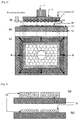
- the driving body for pressure application 10 When the apparatus is driven, the driving body for pressure application 10 is used to pressurize under heating the metal spheres 20 vertically to the substrate surface, and against the fine particle pattern 40 in which fine metal or semiconductor particles are dispersed, or against the fine particle pattern 40 which is formed by fine metal or semiconductor particles adsorbed and fixed onto a viscous substance, where each pattern is coated on a flexible substrate, while at the same time the driving body for pressure application 10 is traveled in an arbitrary direction along the substrate surface within the fine particle pattern 40 to apply sliding stress, and thereby pressure the entire surface of the fine particle pattern 40 efficiently, in order to form a conductive pattern having high electrical conductivity and high electrical characteristics.
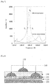
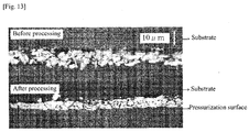
- Fig. 4 (a) taken before the pressurization the antenna wiring patterns are porous and low density is observed.
- Fig. 4 (b) taken after the pressurization on the other hand, voids are virtually non-existent and the density of fine metal particles is high.
- Frequency characteristics of impedance were measured for the same antenna wiring patterns.
- a precision impedance analyzer (4294A) by Agilent was used as the measurement system.
- Fig. 6 shows the impedance characteristics of antenna wiring patterns before and after the pressurization.
- This aluminum paste was coated on a PET substrate with a thickness of 50 ⁇ m, using the blade coating method, after which the coated substrate was heated for 30 minutes at 100°C to volatilize the solvent component, to form a square aluminum patch of I cm x 1 cm in size and approx. 100 ⁇ m in thickness.
- the electrical resistivity was measured using a digital multi-meter (PC500 by Sanwa Electrical Instrument), measurement was not possible (the resistivity was 40 M ⁇ or above).
Landscapes
- Engineering & Computer Science (AREA)
- Manufacturing & Machinery (AREA)
- Microelectronics & Electronic Packaging (AREA)
- Physics & Mathematics (AREA)
- Spectroscopy & Molecular Physics (AREA)
- Dispersion Chemistry (AREA)
- Chemical & Material Sciences (AREA)
- Thermal Sciences (AREA)
- Manufacturing Of Printed Wiring (AREA)
- Parts Printed On Printed Circuit Boards (AREA)
- Exposure Of Semiconductors, Excluding Electron Or Ion Beam Exposure (AREA)
- Manufacturing Of Electric Cables (AREA)
- Electrodes Of Semiconductors (AREA)
Claims (12)
- Film formé en motif conducteur comprenant un motif formé sur un substrat de film (50) ayant une flexibilité par compression, sous chauffage, d'un matériau constitué de particules fines conductrices (70) dispersées et chargées dans une substance visqueuse (60), caractérisé en ce que
le motif conducteur est formé en appliquant une pression dans une direction verticale et horizontale par rapport au matériau constitué de particules fines conductrices (70) dispersé et chargé dans la substance visqueuse (60) sur le substrat de film (50) sous chauffage, dans lequel
par la compression dans une direction verticale et horizontale par rapport au substrat, la masse volumique de la substance visqueuse (60) dans une direction perpendiculaire par rapport à une surface du substrat de film (50) est plus élevée à proximité d'une surface de la substance visqueuse (60) qui entre en contact avec le substrat de film (50) qu'à proximité d'une surface de la substance visqueuse (60) opposée à la surface qui entre en contact avec le substrat de film (50) et ledit motif conducteur ayant une masse volumique des particules fines conductrices (70) changeant dans le motif conducteur dans une direction perpendiculaire à la surface du substrat de film (50) plus faible à proximité d'une surface de la substance visqueuse (60) qui entre en contact avec le substrat de film (50) qu'à proximité d'une surface de la substance visqueuse (60) opposée à la surface qui entre en contact avec le substrat de film (50) de sorte que la résistivité du motif conducteur formé soit diminuée, et par le chauffage, les solvants contenus dans la substance visqueuse sont évaporés, de manière à fixer lesdites particules fines conductrices (70) en position. - Film formé en motif conducteur selon la revendication 1, caractérisé en ce que les particules fines conductrices (70) sont des molécules fines de métal ou semi-conducteur.
- Film formé en motif conducteur selon la revendication 1, caractérisé en ce que les particules fines conductrices (70) ont une taille de particule dans une plage de 10 nm à 10 µm.
- Film formé en motif conducteur selon la revendication 1, caractérisé en ce que les particules fines conductrices (70) sont assemblées ou agrégées sous forme de poudre, que la poudre est telle que les longueurs de son grand axe et son petit axe soient différentes, le grand axe de chaque particule de poudre étant orienté en parallèle avec la surface du substrat (50) et en contact avec les particules de poudre adjacentes, et que les particules fines conductrices (70) qui constituent la poudre contiennent un ou plusieurs matériaux choisis parmi l'argent, l'or, le cuivre, et l'aluminium.
- Film formé en motif conducteur selon la revendication 1, caractérisé en ce que les particules fines conductrices (70) contiennent un ou plusieurs matériaux choisis parmi l'argent, l'or, le cuivre et l'aluminium.
- Film formé en motif conducteur selon la revendication 1, caractérisé en ce que les particules fines de métal qui constituent les particules fines conductrices (70) sont de l'aluminium dans lequel des particules d'additif sont mélangées, lesdites particules d'additif étant des particules de zinc.
- Film formé en motif conducteur selon la revendication 4, caractérisé en ce que la poudre est constituée de particules fines conductrices (70), et les particules fines de métal qui constituent les particules fines conductrices (70) sont de l'aluminium dans lequel des particules d'additif sont mélangées, lesdites particules d'additif étant des particules de zinc.
- Film formé en motif conducteur selon la revendication 1, caractérisé en ce que les particules fines de semi-conducteur qui constituent les particules fines conductrices (70) sont un ou plusieurs matériaux quelconques choisis parmi l'oxyde de zinc, l'oxyde d'indium, l'oxyde de titane, l'oxyde d'étain, l'oxyde de nickel et des composés qui contiennent l'un quelconque de ceux-ci.
- Film formé en motif conducteur selon la revendication 4, caractérisé en ce que la poudre est constituée de particules fines conductrices (70), et les particules fines conductrices (70) sont un ou plusieurs matériaux quelconques choisis parmi l'oxyde de zinc, l'oxyde d'indium, l'oxyde de titane, l'oxyde d'étain, l'oxyde de nickel et des composés qui contiennent l'un quelconque de ceux-ci.
- Film formé en motif conducteur selon la revendication 1, caractérisé en ce que la substance visqueuse (60) est une pâte conductrice qui contient une substance visqueuse (60).
- Film formé en motif conducteur selon la revendication 4, caractérisé en ce que la substance visqueuse (60) est une pâte conductrice qui contient une substance visqueuse (60).
- Procédé de fabrication d'un film formé en motif conducteur comprenant les étapes de :disposition sur un substrat de film (50) d'un matériau constitué de particules fines conductrices (70) dispersées et chargées dans une substance visqueuse (60), caractérisé parl'application de pression dans une direction verticale et horizontale par rapport au matériau constitué des particules fines conductrices (70) dispersées et charges dans la substance visqueuse (60) sous chauffage, dans lequelpar la compression dans une direction verticale et horizontale par rapport au substrat, la masse volumique de la substance visqueuse (60) dans une direction perpendiculaire par rapport à la surface du substrat de film (50) devient plus élevée à proximité de la surface de la substance visqueuse (60) qui entre en contact avec le substrat de film (50) qu'à proximité de la surface de la substance visqueuse (60) opposée à la surface qui entre en contact avec le substrat de film (50) et ledit motif conducteur ayant une masse volumique des particules fines conductrices (70) changeant dans le motif conducteur dans une direction perpendiculaire à la surface du substrat de film (50) plus faible à proximité d'une surface de la substance visqueuse (60) qui entre en contact avec le substrat de film (50) qu'à proximité d'une surface de la substance visqueuse (60) opposée à la surface qui entre en contact avec le substrat de film (50) de sorte que la résistivité du motif conducteur formé soit diminuée, et par le chauffage, les solvants contenus dans la substance visqueuse sont évaporés, de manière à fixer lesdites particules fines conductrices (70) en position.
Applications Claiming Priority (3)
| Application Number | Priority Date | Filing Date | Title |
|---|---|---|---|
| JP2006284445 | 2006-10-19 | ||
| JP2007268168A JP5252473B2 (ja) | 2006-10-19 | 2007-10-15 | 導電パターン形成フィルムと、そのための導電パターン形成方法及び導電パターン形成装置 |
| PCT/JP2007/070230 WO2008047823A1 (fr) | 2006-10-19 | 2007-10-17 | Film de formation d'impression conductrice, et procédé de formation d'impression conductrice et appareil de formation d'impression conductrice pour le film de formation d'impression conductrice |
Publications (3)
| Publication Number | Publication Date |
|---|---|
| EP2075802A1 EP2075802A1 (fr) | 2009-07-01 |
| EP2075802A4 EP2075802A4 (fr) | 2010-11-03 |
| EP2075802B1 true EP2075802B1 (fr) | 2013-11-20 |
Family
ID=39314045
Family Applications (1)
| Application Number | Title | Priority Date | Filing Date |
|---|---|---|---|
| EP07829964.1A Ceased EP2075802B1 (fr) | 2006-10-19 | 2007-10-17 | Film de formation d'impression conductrice, et procédé de formation d'impression conductrice |
Country Status (5)
| Country | Link |
|---|---|
| US (1) | US8278561B2 (fr) |
| EP (1) | EP2075802B1 (fr) |
| JP (1) | JP5252473B2 (fr) |
| KR (1) | KR20090064445A (fr) |
| WO (1) | WO2008047823A1 (fr) |
Families Citing this family (13)
| Publication number | Priority date | Publication date | Assignee | Title |
|---|---|---|---|---|
| US8802387B2 (en) * | 2008-04-30 | 2014-08-12 | Nanyang Technological University | Methods and compounds for detecting beta-lactamase activity |
| US8927054B2 (en) * | 2009-11-24 | 2015-01-06 | National Institute Of Advanced Industrial Science And Technology | Conductive substrate and process for producing same |
| US9412623B2 (en) * | 2011-06-08 | 2016-08-09 | Cbrite Inc. | Metal oxide TFT with improved source/drain contacts and reliability |
| US8679905B2 (en) * | 2011-06-08 | 2014-03-25 | Cbrite Inc. | Metal oxide TFT with improved source/drain contacts |
| TW201339279A (zh) * | 2011-11-24 | 2013-10-01 | Showa Denko Kk | 導電圖型形成方法及藉由光照射或微波加熱的導電圖型形成用組成物 |
| CN104885576B (zh) * | 2012-12-31 | 2017-12-05 | 阿莫绿色技术有限公司 | 柔性印刷电路基板及其制造方法 |
| KR101560268B1 (ko) * | 2014-04-21 | 2015-10-14 | 경희대학교 산학협력단 | 플렉서블 기판용 배리어 막 형성 방법 |
| US10235061B1 (en) * | 2016-09-26 | 2019-03-19 | EMC IP Holding Company LLC | Granular virtual machine snapshots |
| WO2019125488A1 (fr) * | 2017-12-22 | 2019-06-27 | Hewlett-Packard Development Company, L.P. | Codage dans des objets tridimensionnels |
| CN108718479A (zh) * | 2018-07-13 | 2018-10-30 | 上海德门信息技术有限公司 | 一种液晶聚合物银浆的柔性电路基板及其制备方法和应用 |
| JP7667960B2 (ja) * | 2020-05-01 | 2025-04-24 | 大日本印刷株式会社 | 配線基板及び配線基板の製造方法 |
| CN216930463U (zh) * | 2021-10-09 | 2022-07-08 | 北京梦之墨科技有限公司 | 一种lcp电路板、多层lcp电路板及电子器件 |
| CN114783298B (zh) * | 2022-05-25 | 2023-08-01 | 苏州华星光电技术有限公司 | 柔性屏的校平装置和柔性屏的校平方法 |
Citations (3)
| Publication number | Priority date | Publication date | Assignee | Title |
|---|---|---|---|---|
| US6238597B1 (en) * | 1999-03-10 | 2001-05-29 | Korea Advanced Institute Of Science And Technology | Preparation method of anisotropic conductive adhesive for flip chip interconnection on organic substrate |
| US20030213614A1 (en) * | 2002-04-15 | 2003-11-20 | Masahiro Furusawa | Conductive layer pattern and method for forming the same, wiring board, electronic device, electronic appliances and noncontact card medium |
| EP1398673A2 (fr) * | 2002-09-12 | 2004-03-17 | Canon Kabushiki Kaisha | Développeur |
Family Cites Families (21)
| Publication number | Priority date | Publication date | Assignee | Title |
|---|---|---|---|---|
| DE1200405B (de) | 1956-09-28 | 1965-09-09 | Nippon Telegraph & Telephone | Verfahren zur Herstellung einer elektrisch leitenden Schicht auf Oberflaechen |
| JPS59195837A (ja) * | 1983-04-21 | 1984-11-07 | Sharp Corp | Lsiチツプボンデイング方法 |
| US4960614A (en) * | 1987-02-06 | 1990-10-02 | Key-Tech, Inc. | Printed circuit board |
| JPH03152992A (ja) * | 1989-10-27 | 1991-06-28 | W R Grace & Co | 印刷回路板及びその製造方法 |
| EP0452118B1 (fr) * | 1990-04-12 | 1996-08-21 | Matsushita Electric Industrial Co., Ltd. | Composition d'encre conductrice et méthode pour former un dessin conducteur en couche épaisse |
| DE69216658T2 (de) | 1991-02-25 | 1997-08-07 | Canon Kk | Vorrichtung und Verfahren zur Verbindung elektrischer Bauelemente |
| US5197655A (en) * | 1992-06-05 | 1993-03-30 | International Business Machines Corporation | Fine pitch solder application |
| US6034331A (en) * | 1996-07-23 | 2000-03-07 | Hitachi Chemical Company, Ltd. | Connection sheet and electrode connection structure for electrically interconnecting electrodes facing each other, and method using the connection sheet |
| JP2000113919A (ja) * | 1998-08-03 | 2000-04-21 | Sony Corp | 電気的接続装置と電気的接続方法 |
| JP2000195584A (ja) * | 1998-12-25 | 2000-07-14 | Sony Corp | 電気的接続装置と電気的接続方法 |
| JP2001064547A (ja) * | 1999-09-01 | 2001-03-13 | Toyo Ink Mfg Co Ltd | 活性エネルギー線硬化型導電性ペースト、それを用いた導体回路および非接触id |
| JP2001135138A (ja) * | 1999-10-29 | 2001-05-18 | Matsushita Electric Ind Co Ltd | 導体ペースト |
| JP2001243836A (ja) | 1999-12-21 | 2001-09-07 | Murata Mfg Co Ltd | 導電性ペースト及びそれを用いた印刷配線板 |
| JP2003089282A (ja) * | 2001-09-18 | 2003-03-25 | Fuji Xerox Co Ltd | スクリーン印刷版及びその製造方法、スクリーン印刷版の製造装置、スクリーン印刷方法、スクリーン印刷装置、並びにスクリーン印刷物 |
| US20040178391A1 (en) | 2003-01-29 | 2004-09-16 | Conaghan Brian F. | High conductivity inks with low minimum curing temperatures |
| JP4414145B2 (ja) | 2003-03-06 | 2010-02-10 | ハリマ化成株式会社 | 導電性ナノ粒子ペースト |
| WO2005002002A1 (fr) * | 2003-06-25 | 2005-01-06 | Hitachi Chemical Co., Ltd. | Materiau de connexion de circuit, materiau de connexion de circuit de type film, faisant appel a ce dernier, structure de connexion d'elements de circuit et son procede de production |
| US20050153107A1 (en) * | 2004-01-12 | 2005-07-14 | Tdk Corporation | Substrate having functional layer pattern formed thereon and method of forming functional layer pattern |
| JP2005259848A (ja) | 2004-03-10 | 2005-09-22 | Toshiba Corp | 半導体装置及びその製造方法 |
| JP2006024485A (ja) * | 2004-07-09 | 2006-01-26 | Mitsubishi Paper Mills Ltd | 導電性膜または導電性画像作製方法 |
| JP4934993B2 (ja) * | 2005-05-25 | 2012-05-23 | 住友電気工業株式会社 | 導電性ペーストおよびそれを用いた配線基板 |
-
2007
- 2007-10-15 JP JP2007268168A patent/JP5252473B2/ja not_active Expired - Fee Related
- 2007-10-17 EP EP07829964.1A patent/EP2075802B1/fr not_active Ceased
- 2007-10-17 US US12/443,482 patent/US8278561B2/en not_active Expired - Fee Related
- 2007-10-17 WO PCT/JP2007/070230 patent/WO2008047823A1/fr not_active Ceased
- 2007-10-17 KR KR1020097007319A patent/KR20090064445A/ko not_active Ceased
Patent Citations (3)
| Publication number | Priority date | Publication date | Assignee | Title |
|---|---|---|---|---|
| US6238597B1 (en) * | 1999-03-10 | 2001-05-29 | Korea Advanced Institute Of Science And Technology | Preparation method of anisotropic conductive adhesive for flip chip interconnection on organic substrate |
| US20030213614A1 (en) * | 2002-04-15 | 2003-11-20 | Masahiro Furusawa | Conductive layer pattern and method for forming the same, wiring board, electronic device, electronic appliances and noncontact card medium |
| EP1398673A2 (fr) * | 2002-09-12 | 2004-03-17 | Canon Kabushiki Kaisha | Développeur |
Also Published As
| Publication number | Publication date |
|---|---|
| EP2075802A4 (fr) | 2010-11-03 |
| JP2008124446A (ja) | 2008-05-29 |
| WO2008047823A1 (fr) | 2008-04-24 |
| EP2075802A1 (fr) | 2009-07-01 |
| US20100025088A1 (en) | 2010-02-04 |
| US8278561B2 (en) | 2012-10-02 |
| JP5252473B2 (ja) | 2013-07-31 |
| KR20090064445A (ko) | 2009-06-18 |
Similar Documents
| Publication | Publication Date | Title |
|---|---|---|
| EP2075802B1 (fr) | Film de formation d'impression conductrice, et procédé de formation d'impression conductrice | |
| US8105126B2 (en) | Method for fabricating touch panel | |
| KR101611379B1 (ko) | 편광판 정전용량 방식 터치 스크린 | |
| CN107272978B (zh) | 触屏传感器 | |
| Huang et al. | Selective deposition of films of polypyrrole, polyaniline and nickel on hydrophobic/hydrophilic patterned surfaces and applications | |
| EP3028126B1 (fr) | Fixation de composants électroniques à des conducteurs imprimés transparents à base de nanofils | |
| US20140055688A1 (en) | Polarizer resistive touch screen | |
| EP2991083B1 (fr) | Procédé de fabrication d'un motif électroconducteur et substrat sur lequel est formé un motif électroconducteur | |
| US20150277646A1 (en) | Pressure-sensitive element, method of producing the pressure-sensitive element, touch panel equipped with the pressure-sensitive element, and method of producing the pressure-sensitive element | |
| EP3190488A1 (fr) | Corps de câblage, carte de câblage, capteur tactile et procédé de production de corps de câblage | |
| EP3451132A1 (fr) | Corps de câblage, ensemble corps de câblage, substrat de câblage et capteur tactile | |
| EP3190492A1 (fr) | Ensemble élément de câblage, structure ayant une couche conductrice, et capteur de toucher | |
| US20160198527A1 (en) | Transparent film heater and manufacturing method thereof | |
| WO2014186533A1 (fr) | Films à base de nanostructures conductrices présentant des performances esd améliorées | |
| JP2012151095A (ja) | 透明導電性フィルム、静電容量式タッチパネルの透明電極及びタッチパネル | |
| CN102820072B (zh) | 导电性糊剂 | |
| JPH05143219A (ja) | 透明入力パネル | |
| KR20160061469A (ko) | 지지체를 이용한 은나노와이어 투명전극 제조방법 | |
| TW200928938A (en) | Panel-type input device | |
| JP2013202911A (ja) | 透明導電層付き基体の製造方法 | |
| CN207008580U (zh) | 具有由多个层制造的触摸屏的移动通信设备 | |
| CN102819340B (zh) | 触摸屏面板的制备方法 | |
| JP2017163085A (ja) | 接合体の製造方法 | |
| US11961632B2 (en) | Fabrication method of conductive nanonetworks using mastermold | |
| Rohit | Optimization and characterization of a capillary contact micro-plotter for printed electronic devices |
Legal Events
| Date | Code | Title | Description |
|---|---|---|---|
| PUAI | Public reference made under article 153(3) epc to a published international application that has entered the european phase |
Free format text: ORIGINAL CODE: 0009012 |
|
| 17P | Request for examination filed |
Effective date: 20090325 |
|
| AK | Designated contracting states |
Kind code of ref document: A1 Designated state(s): AT BE BG CH CY CZ DE DK EE ES FI FR GB GR HU IE IS IT LI LT LU LV MC MT NL PL PT RO SE SI SK TR |
|
| AX | Request for extension of the european patent |
Extension state: AL BA HR MK RS |
|
| A4 | Supplementary search report drawn up and despatched |
Effective date: 20101006 |
|
| DAX | Request for extension of the european patent (deleted) | ||
| RBV | Designated contracting states (corrected) |
Designated state(s): DE FR GB |
|
| 17Q | First examination report despatched |
Effective date: 20121008 |
|
| REG | Reference to a national code |
Ref country code: DE Ref legal event code: R079 Ref document number: 602007033942 Country of ref document: DE Free format text: PREVIOUS MAIN CLASS: H01B0005140000 Ipc: H05K0001030000 |
|
| RIC1 | Information provided on ipc code assigned before grant |
Ipc: H05K 1/03 20060101AFI20130424BHEP Ipc: H05K 3/10 20060101ALI20130424BHEP Ipc: H05K 3/12 20060101ALI20130424BHEP |
|
| GRAP | Despatch of communication of intention to grant a patent |
Free format text: ORIGINAL CODE: EPIDOSNIGR1 |
|
| INTG | Intention to grant announced |
Effective date: 20130604 |
|
| GRAS | Grant fee paid |
Free format text: ORIGINAL CODE: EPIDOSNIGR3 |
|
| GRAA | (expected) grant |
Free format text: ORIGINAL CODE: 0009210 |
|
| AK | Designated contracting states |
Kind code of ref document: B1 Designated state(s): DE FR GB |
|
| REG | Reference to a national code |
Ref country code: GB Ref legal event code: FG4D |
|
| REG | Reference to a national code |
Ref country code: DE Ref legal event code: R096 Ref document number: 602007033942 Country of ref document: DE Effective date: 20140116 |
|
| REG | Reference to a national code |
Ref country code: DE Ref legal event code: R097 Ref document number: 602007033942 Country of ref document: DE |
|
| PLBE | No opposition filed within time limit |
Free format text: ORIGINAL CODE: 0009261 |
|
| STAA | Information on the status of an ep patent application or granted ep patent |
Free format text: STATUS: NO OPPOSITION FILED WITHIN TIME LIMIT |
|
| 26N | No opposition filed |
Effective date: 20140821 |
|
| REG | Reference to a national code |
Ref country code: DE Ref legal event code: R097 Ref document number: 602007033942 Country of ref document: DE Effective date: 20140821 |
|
| REG | Reference to a national code |
Ref country code: FR Ref legal event code: PLFP Year of fee payment: 10 |
|
| REG | Reference to a national code |
Ref country code: FR Ref legal event code: PLFP Year of fee payment: 11 |
|
| REG | Reference to a national code |
Ref country code: FR Ref legal event code: PLFP Year of fee payment: 12 |
|
| PGFP | Annual fee paid to national office [announced via postgrant information from national office to epo] |
Ref country code: FR Payment date: 20180808 Year of fee payment: 12 |
|
| PGFP | Annual fee paid to national office [announced via postgrant information from national office to epo] |
Ref country code: GB Payment date: 20180807 Year of fee payment: 12 |
|
| PGFP | Annual fee paid to national office [announced via postgrant information from national office to epo] |
Ref country code: DE Payment date: 20180806 Year of fee payment: 12 |
|
| REG | Reference to a national code |
Ref country code: DE Ref legal event code: R119 Ref document number: 602007033942 Country of ref document: DE |
|
| PG25 | Lapsed in a contracting state [announced via postgrant information from national office to epo] |
Ref country code: DE Free format text: LAPSE BECAUSE OF NON-PAYMENT OF DUE FEES Effective date: 20200501 |
|
| GBPC | Gb: european patent ceased through non-payment of renewal fee |
Effective date: 20191017 |
|
| PG25 | Lapsed in a contracting state [announced via postgrant information from national office to epo] |
Ref country code: FR Free format text: LAPSE BECAUSE OF NON-PAYMENT OF DUE FEES Effective date: 20191031 Ref country code: GB Free format text: LAPSE BECAUSE OF NON-PAYMENT OF DUE FEES Effective date: 20191017 |