EP2077585A1 - Element de batterie solaire et procede de fabrication associe - Google Patents
Element de batterie solaire et procede de fabrication associe Download PDFInfo
- Publication number
- EP2077585A1 EP2077585A1 EP07828791A EP07828791A EP2077585A1 EP 2077585 A1 EP2077585 A1 EP 2077585A1 EP 07828791 A EP07828791 A EP 07828791A EP 07828791 A EP07828791 A EP 07828791A EP 2077585 A1 EP2077585 A1 EP 2077585A1
- Authority
- EP
- European Patent Office
- Prior art keywords
- silicon substrate
- solar cell
- cell element
- electrode
- element according
- Prior art date
- Legal status (The legal status is an assumption and is not a legal conclusion. Google has not performed a legal analysis and makes no representation as to the accuracy of the status listed.)
- Withdrawn
Links
Images


Classifications
-
- H—ELECTRICITY
- H10—SEMICONDUCTOR DEVICES; ELECTRIC SOLID-STATE DEVICES NOT OTHERWISE PROVIDED FOR
- H10F—INORGANIC SEMICONDUCTOR DEVICES SENSITIVE TO INFRARED RADIATION, LIGHT, ELECTROMAGNETIC RADIATION OF SHORTER WAVELENGTH OR CORPUSCULAR RADIATION
- H10F77/00—Constructional details of devices covered by this subclass
- H10F77/20—Electrodes
- H10F77/206—Electrodes for devices having potential barriers
- H10F77/211—Electrodes for devices having potential barriers for photovoltaic cells
-
- H—ELECTRICITY
- H10—SEMICONDUCTOR DEVICES; ELECTRIC SOLID-STATE DEVICES NOT OTHERWISE PROVIDED FOR
- H10F—INORGANIC SEMICONDUCTOR DEVICES SENSITIVE TO INFRARED RADIATION, LIGHT, ELECTROMAGNETIC RADIATION OF SHORTER WAVELENGTH OR CORPUSCULAR RADIATION
- H10F71/00—Manufacture or treatment of devices covered by this subclass
- H10F71/121—The active layers comprising only Group IV materials
-
- Y—GENERAL TAGGING OF NEW TECHNOLOGICAL DEVELOPMENTS; GENERAL TAGGING OF CROSS-SECTIONAL TECHNOLOGIES SPANNING OVER SEVERAL SECTIONS OF THE IPC; TECHNICAL SUBJECTS COVERED BY FORMER USPC CROSS-REFERENCE ART COLLECTIONS [XRACs] AND DIGESTS
- Y02—TECHNOLOGIES OR APPLICATIONS FOR MITIGATION OR ADAPTATION AGAINST CLIMATE CHANGE
- Y02E—REDUCTION OF GREENHOUSE GAS [GHG] EMISSIONS, RELATED TO ENERGY GENERATION, TRANSMISSION OR DISTRIBUTION
- Y02E10/00—Energy generation through renewable energy sources
- Y02E10/50—Photovoltaic [PV] energy
- Y02E10/547—Monocrystalline silicon PV cells
-
- Y—GENERAL TAGGING OF NEW TECHNOLOGICAL DEVELOPMENTS; GENERAL TAGGING OF CROSS-SECTIONAL TECHNOLOGIES SPANNING OVER SEVERAL SECTIONS OF THE IPC; TECHNICAL SUBJECTS COVERED BY FORMER USPC CROSS-REFERENCE ART COLLECTIONS [XRACs] AND DIGESTS
- Y02—TECHNOLOGIES OR APPLICATIONS FOR MITIGATION OR ADAPTATION AGAINST CLIMATE CHANGE
- Y02P—CLIMATE CHANGE MITIGATION TECHNOLOGIES IN THE PRODUCTION OR PROCESSING OF GOODS
- Y02P70/00—Climate change mitigation technologies in the production process for final industrial or consumer products
- Y02P70/50—Manufacturing or production processes characterised by the final manufactured product
Definitions
- the present invention relates to a solar cell element and a method for manufacturing the same.
- Solar cell elements convert solar energy into electrical energy.
- a known solar cell element includes a silicon substrate having a light-reception surface and a back surface and electrodes mainly containing aluminum formed on the surface of the silicon substrate.
- Patent Document 1 Japanese Unexamined Patent Application Publication No. 2003-223813
- the solar cell element is expected to spread more widely, and it is accordingly important for the solar cell element to exhibit high conversion efficiency. In order to increase the conversion efficiency, it is important to reduce the warp of the silicon substrate and to increase the adhesion between the silicon substrate and the electrode.
- an object of the invention is to provide a high-performance solar cell element.
- a solar cell element of the invention includes a silicon substrate, and a first electrode formed of aluminum and a metal containing zinc on the silicon substrate.
- the solar cell element of the invention includes an electrode formed on aluminum and a metal containing zinc on a silicon substrate.
- the warp of the silicon substrate resulting from the difference in thermal expansion coefficient between the silicon substrate and aluminum can be alleviated to prevent the reduction of the adhesion between the electrode and the silicon substrate.
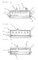
- Fig. 1 is a sectional view of a solar cell element according to an embodiment.
- Fig. 2(a) is a plan view of a first surface (light-reception surface) of the solar cell element shown in Fig. 1
- Fig. 2(b) is a plan view of a second surface (opposite to the light-reception surface) of the solar cell element shown in Fig. 1 .
- the solar cell element of the present embodiment includes a silicon substrate 1 having a first surface (light-reception surface) and a second surface (back surface), and a first electrode formed of aluminum and a metal containing zinc on the silicon substrate 1.
- the first electrode is disposed on the second surface of the silicon substrate 1. This structure can alleviate the warp of the silicon substrate 1 even if the silicon substrate 1 has a small thickness of, for example, 200 ⁇ m or less.
- the silicon substrate 1 having a first conductivity type has a front surface electrode 4 and a back surface electrode 5.
- the back surface electrode 5 includes current-collector portions (first electrodes) 5a and power-extracting portions (second electrodes) 5b through which the electricity collected through the current-collector portion 5a is extracted.
- the first surface of the silicon substrate 1 has a diffusion layer 2 having a second conductivity type and an antireflection coating 3.
- the second surface of the silicon substrate 1 has a back surface electric field region 6.
- the solar cell element When light enters the solar cell element from the light-reception surface side, the light is mainly absorbed by the bulk region of the silicon substrate 1, which is a p-type semiconductor, and converted into electricity to produce electron-hole pairs (electron carriers and hole carriers).
- the electron carriers and hole carriers act as the photo-excitation source (photo-production carriers) and generate a photoelectromotive force in the solar cell element.
- the antireflection coating 3 reduces the reflectance of the light in a desired wavelength region depending on the refractive index and the thickness of the film defining the antireflection coating, and thus increases the amount of photo-production carriers to increase the photocurrent density Jsc of the solar cell element.
- the silicon substrate 1 has current-collector portions 5a (first electrodes) being fired electrodes mainly made of aluminum.
- the current-collector portions 5a also contain externally added inorganic particles having a lower melting point than aluminum.
- the inorganic particles are made of a metal containing zinc.
- the current-collector portion 5a mainly made of aluminum mentioned herein means that the current-collector portion 5a contains a higher weight of aluminum than that of the inorganic particles.
- the current-collector portion 5a containing externally added inorganic particles means that an electroconductive paste being the electrode material contains the inorganic particles.
- the warp of the solar cell element resulting from the difference in thermal expansion coefficient between the silicon substrate 1 and the current-collector portion 5a can be reduced, and besides the adhesion between the current-collector portion 5a and the silicon substrate 1 can be prevented from decreasing.
- the inorganic particles are zinc or a zinc alloy
- the resistance loss of the current-collector portions 5a can be reduced more than that of the known electrode made of aluminum paste containing SiO 2 , Al 2 O 3 or the like.
- the decrease in FF value fill factor
- the decrease in FF value fill factor
- the current-collector portions 5a are formed over substantially the entire main surface of the silicon substrate except the regions of the power-extracting portions 5b.
- aluminum which is a p-type dopant element, is sufficiently diffused in the back surface of the silicon substrate 1 to form a back surface electric field region 6 (BSF region) over substantially the entire back surface of the solar cell element. Consequently, the open-circuit voltage Voc can be increased by the BSF effect, and the element efficiency can be increased accordingly.
- the adhesion between the silicon substrate 1 and the current-collector portions 5a can further be enhanced. Consequently, the reduction in output power, which is caused by separation of the current-collector portions 5a from the silicon substrate 1, can further be prevented.
- the current-collector portion 5a contains 3 to 50 parts by weight of zinc or zinc alloy relative to 100 parts by weight of aluminum.
- the warp of the silicon substrate 1 can sufficiently be reduced in addition to the above-described advantage. Consequently, the values of the adhesion, the electroconductivity, and the output power can simultaneously be favorable to form a more sufficient back surface electric field region 6 (BSF region).
- the warp of the silicon substrate can be reduced without affecting the performance.
- zinc element can be measured by EPMA, for example.
- the silicon substrate 1 used in the embodiment is made of, for example, monocrystalline silicon or polycrystalline silicon containing a semiconductor dopant, such as boron (B).
- the silicon substrate 1 made of polycrystalline silicon can be mass-produced.
- Such a silicon substrate 1 is produced by cutting an ingot produced by a crystal pulling method or casting into pieces of about 10 cm x 10 cm to 25 cm x 25 cm and slicing the pieces to a thickness of 500 ⁇ m or less, preferably 250 ⁇ m or less.
- the cut surface of the silicon substrate 1 is very slightly etched to clean with NaOH or KOH, or hydrofluoric acid or fluoronitric acid.
- a uneven (rough surface) structure is formed in the surface of the silicon substrate 1 through which sunlight enters. If the light-reception surface of the silicon substrate 1 is rough and has asperities, sunlight is prevented from reflecting from the light-reception surface of the silicon substrate 1.
- a diffusion layer 2 having a second conductivity type is formed in the light-reception surface of the silicon substrate 1 to form a pn junction between the diffusion layer and the bulk region of the silicon substrate.
- the diffusion layer 2 acts as an n-type layer 2.
- a Group V element is used as the n-doping element, such as phosphorus (P), and an n+ type layer having a sheet resistance of about 30 to 300 ohms per square is formed.
- the first conductivity type is the n type
- the diffusion layer 2 acts as a p-type layer 2.
- a Group III element is used as the p-doping element, such as boron (B).
- P+ or n+ means that the dopant content is high.
- the diffusion layer 2 is formed, for example, by a thermal diffusion coating in which the surface of the silicon substrate 1 is coated with a P 2 O 5 paste, by gas phase thermal diffusion using POCl 3 (phosphoryl chloride) gas as a diffusion source, or by ion implantation in which p+ ions are directly diffused.
- the diffusion layer 2 has a depth of about 0.2 to 0.5 ⁇ m. If a diffusion region is formed in the surface opposite the intended surface, the area for the diffusion region may be coated with an anti-diffusion film in advance and etched later.
- the diffusion layer except the diffusion layer 2 formed in the front surface of the silicon substrate 1 can be removed by etching with hydrofluoric acid or a mixture of hydrofluoric acid and nitric acid with the front surface of the silicon substrate 1 coated with a resist film and then the resist is removed.
- the formation of the diffusion layer 2 is not limited to the above-described method.
- a hydrogenated amorphous silicon layer or a crystalline silicon layer including a microcrystalline silicon layer may be formed by a process and under conditions for forming thin films.
- an i-type silicon region may be formed between the silicon substrate 1 and the diffusion layer 2.
- the material of the antireflection coating 3 may be a SiNx film (having a range of compositions around the Si 3 N 4 stoichiometric composition), a TiO 2 film, a SiO 2 film, a MgO film, an ITO film, a SnO 2 film, a ZnO film and so on. If the antireflection coating 3 formed over the silicon substrate 1 has a refractive index of about 1.8 to 2.3 and a thickness of about 500 to 1200 ⁇ , light reflection can be reduced effectively.
- Such an antireflection coating 3 may be formed by PECVD, vapor deposition, sputtering or the like.
- the antireflection coating 3 is formed into a predetermined pattern for forming the front surface electrodes 4.
- the patterning may be performed by etching using, for example, a resist mask (wet etching or dry etching), or by forming a mask in advance of the formation of the antireflection coating 3 and removing the mask after the completion of the antireflection coating 3. If a so-called fire-through method is applied, patterning is not necessary.
- the front surface electrodes 4 and the diffusion layer 2 are brought into electrical contact with each other by applying an electrode paste for the front surface electrodes 4 onto the antireflection coating 3 and then firing the paste. Since the fire-through method is applied to the structure shown in Fig. 2(a) , patterning is not performed.
- a back surface electric field region (BSF region) 6 is formed in the back surface of the silicon substrate 1.
- the BSF region contains a dopant in a higher concentration than the silicon substrate 1.
- the first conductivity type is the p type
- boron or aluminum is used as the dopant element to form a p+ type region. Consequently, the carrier recombination loss can be reduced in the vicinity of the back surface of the silicon substrate 1.
- Photo-production carriers generated in the vicinity of the back surface of the silicon substrate 1 are accelerated by the electric field, and consequently electric power is extracted effectively and the photosensitivity particularly to long wavelength light is enhanced. Accordingly, the photocurrent density Jsc is increased, and the minority carrier (electron) density is reduced in the back surface electric field region 6 (BSF region).
- the amount of diode current dark current
- Voc open-circuit voltage
- Such a back surface electric field region 6 can be formed by diffusing a first conductivity type dopant at a high concentration into the silicon substrate 1.
- a diffusion barrier is formed of, for example, an oxide layer over the diffusion layer 2 in advance.
- the back surface electric field region 6 is formed by thermal diffusion using BBr 3 (boron tribromide) as the diffusion source at a temperature of about 800 to 1100°C.
- BBr 3 boron tribromide
- an electroconductive paste containing aluminum powder and an organic vehicle is applied by printing and then heat-treating (firing) the paste at a temperature of about 700 to 850°C. The aluminum is thus diffused into the silicon substrate 1 to form the back surface electric field region 6.
- the process of printing the electroconductive paste, followed by firing can form a desired diffusion region in a printed surface, and, in addition, does not require the removal of the diffusion layer formed in the back surface simultaneously with the formation of the diffusion layer 2 as described above and having the opposite conductivity type, or the n type.
- the front surface electrodes 4 and the back surface electrode 5 including the current-collector portions 5a (first electrode) and the power-extracting portions 5b (second electrode) are formed on the surfaces of the silicon substrate 1, as below.
- the back surface electrode 5 is in ohmic contact with the BSF layer 4.
- a silver paste prepared by adding 10 to 30 parts by weight of organic vehicle and 0.1 to 5 parts by weight of glass frit to 100 parts by weight of metal powder containing silver or the like is applied to form a predetermined electrode shape, such as a grid shape, as shown in Fig. 2(a) , and fired at the maximum temperature of 600 to 850°C for several tens of seconds to several tens of minutes, thereby forming the electrodes.
- the paste can be applied by screen printing. After the application, preferably, the solvent is vaporized at a predetermined temperature to dry.
- an electroconductive paste containing a metal material containing zinc, aluminum and an organic vehicle is applied over substantially the entire surface of the back surface except the regions in which the power-extracting portions 5b are to be formed, as shown in Fig. 2(b) .
- the paste can be applied by screen printing. After the application, preferably, the solvent is vaporized at a predetermined temperature to dry.
- an electroconductive paste prepared by adding 10 to 30 parts by weight of organic vehicle and 0.1 to 5 parts by weight of glass frit to 100 parts by weight of metal powder containing silver powder or the like is applied to form the electrode shape shown in Fig. 2(b) , in the same manner as the formation of the front surface electrodes 4.
- the silver paste is applied to positions at which the silver paste partially comes into contact with the electroconductive paste so as to overlap and intersect the current-collector portion 5a and the power-extracting portions 5b.
- the silver paste can be applied by screen printing or other known methods.
- the solvent is vaporized at a predetermined temperature to dry.
- the organic vehicle can be prepared by dissolving at least one resin selected from the group including cellulose resins, such as methyl cellulose, ethyl cellulose and nitro cellulose, acrylic resins, such as methyl methacrylate, and butyral resins in an organic solvent, such as butyl carbitol, butyl carbitol acetate, butyl cellosolve, butyl cellosolve acetate, terpineol, hydrogenated terpineol, hydrogenated terpineol acetate, methyl ethyl ketone, isobonyl acetate, or nopyl acetate.
- cellulose resins such as methyl cellulose, ethyl cellulose and nitro cellulose
- acrylic resins such as methyl methacrylate
- butyral resins in an organic solvent, such as butyl carbitol, butyl carbitol acetate, butyl cellosolve, butyl cellosolve acetate
- the glass frit is preferably glass containing PbO 2 , B 2 O 3 , SiO 2 , ZnO or the like from the viewpoint of enhancing the adhesion between the electrode and the silicon substrate 1.
- the glass frit can be added in an amount of about 0.1 to 5 parts by weight relative to 100 parts by weight of aluminum.
- Preferred glass frit content is 1.5 parts by weight or less because a higher glass frit content tends to increase the warp.
- the pastes are dried in a drying oven, and then fired at a maximum temperature of 700 to 850°C for several tens of seconds to several tens of minutes in a firing oven, thereby forming the back surface electrode 5 (current-collector portions 5a and power-extracting portions 5b).
- the electroconductive paste used in the present invention contains an inorganic material and aluminum.
- the inorganic material is a metal material having a melting point lower than aluminum and containing zinc.
- Constaining zinc mentioned herein means that the metal material is constituted of zinc or a zinc alloy.
- aluminum has a melting point of 660.4°C
- zinc used as the inorganic material has a melting point of 419.6°C.
- the particles of the inorganic material can have such a size as can pass through, for example, a 75 ⁇ m mesh screen.
- the mean particle size is preferably 30 ⁇ m or less, and more preferably 15 ⁇ m or less.
- the aluminum and inorganic material contained in the electroconductive paste may be powder in a form of spheres, flakes or formless shapes.
- Such aluminum can be powder having a mean particle size of, for example, about 3 to 20 ⁇ m, and 10 to 30 parts by weight of organic vehicle can be added to 100 parts by weight of aluminum.
- the paste may contain a glass frit in a proportion of 0.1 to 5 parts by weight to 100 parts by weight of aluminum.
- the method for manufacturing the solar cell element includes the first step of applying the electroconductive paste onto the silicon substrate 1.
- the application can be performed by various methods including screen printing, a roll coater method and dispenser method.
- the second step is performed of firing the electroconductive paste at a temperature higher than the melting point of the inorganic material. More specifically, the paste is fired at a maximum temperature of 700 to 850°C for several tens of seconds to several tens minutes in a firing oven, thus forming the current-collector portions 5a.
- the zinc-containing metal material in the electroconductive paste is brought into a state of liquid phase by firing at a temperature higher than its melting point in the second step. Therefore the zinc-containing metal material keeps liquid phase at temperatures between its melting point and the maximum firing temperature.
- the metal material containing zinc in a liquid phase flows (spread) so as to compensate for the reduction in volume of aluminum during cooling from the maximum firing temperature to the melting point of the zinc-containing metal material, and thus alleviates the reduction in total volume of the paste that can be caused by cooling.
- the particles of the aluminum powder are joined to each other with the inorganic material.
- the warp of the silicon substrate can be alleviated which results from the difference in thermal expansion coefficient between the silicon substrate and the aluminum.
- rapid heating and rapid cooling are performed from the viewpoint of increasing the output power of the solar cell.
- heating and cooling are performed at a rate of 20°C/s or more, and the retention time of the peak temperature is several seconds. If rapid cooling is performed at a rate of 30°C/s or more, the warp of the silicon substrate can be increased after firing.
- the present invention can sufficiently reduce the warp even if rapid cooling is performed.
- the rates of heating and cooling can be calculated from the gradient of the profile (temperature-time) of temperatures before and after reaching a peak temperature, measured with a thermocouple attached to the silicon substrate 1.
- the electrode made of the zinc-containing metal and aluminium after the second step can prevent the reduction of the adhesion between the current-collector portions 5a and the silicon substrate 1.
- the electroconductive paste contains 3 to 50 parts by weight of at least one of zinc powder and a zinc alloy powder relative to 100 parts by weight of aluminum powder. If the zinc or zinc alloy content is 3 parts by weight or more, the above-described effects can be produced more favorably.
- the firing oven includes a furnace body 21 having an internal space, a transport mechanism 25 transporting a work placed thereon to be heated from a transport entrance 23 to a transport exit 24 in the furnace body, and heating means (for example, infrared ray lamp) 27 disposed to an upper side of the transport mechanism 25 for heating the work.
- heating means for example, infrared ray lamp
- an exhaust unit 28 is provided at the ceiling of the furnace body 21 for discharging the solvent vaporized from the heated work to the outside of the furnace body 21 and additional heating means 27 are further provided in the firing oven for heating the ceiling of the furnace body 21 and the exhaust unit 28.
- the furnace body 21 has a double structure made of a heat-resistant and corrosion-resistant metal, such as stainless steel, and a heat insulator is disposed in the gap in the double structure.
- the furnace body 21 has openings for the transport entrance 23 and transport exit 24 through which the belt of the transport mechanism 25 transports the work 22 thereon between the internal space of the furnace body 21 and the external space.
- the belt is turned around by a rotating roller at the position from which the belt protrudes to the outside of the furnace body.
- a sensor or a buzzer including, for example, a photo interpreter or a proximity sensor may be disposed to indicate whether the work 22 comes in or out, in the vicinity of the transport entrance 23 and the transport exit 24.
- the transport mechanism 25 includes a mesh belt or a zonal belt made of, for example, an alloy composition, such as stainless steel alloy, Ni-Cr alloy or an alloy of manganese, molybdenum, titanium, aluminum, niobium, chromium, zirconium or boron, a rotating roller 31 for turning around the belt at both ends in the running direction of the belt, a driving roller 32 for transmitting a driving force for transport to the belt, a servomotor (not shown) for generating the driving force, and a connection chain (not shown) for connecting the driving roller 32 and the servomotor. Both ends of the belt are connected to form a ring so as to round endlessly in the transporting direction.
- an alloy composition such as stainless steel alloy, Ni-Cr alloy or an alloy of manganese, molybdenum, titanium, aluminum, niobium, chromium, zirconium or boron
- a rotating roller 31 for turning around the belt at both ends in the running direction of the belt
- An angular velocity sensor such as of a rotary encoder, is provided to the servomotor, the driving roller 32 and/or the rotating roller 31 to detect the angular velocity of the shaft, and further the transporting speed, one after another.
- the servomotor and/or the angular velocity sensor is electrically connected to an arithmetic processing unit with a signal line not shown in the figure so as to sequentially detect the transporting speed according to the input signal from the arithmetic processing unit and/or the output to the arithmetic processing unit and controls the transporting speed to a predetermined speed.
- the infrared ray lamp 27 being a heating means is electrically connected to a power source disposed outside the furnace body 21 with a power cable (not shown), and receives an alternating current power or a direct current powder applied from the power source, thereby being heated to emit infrared rays, such as far infrared rays or near infrared rays.
- At least one infrared ray lamp is arranged, for example, in a line, an array, or an arch manner inside the furnace body.
- the infrared ray lamp 27 includes a heating/light-emitting member generating heat or emitting light by energization, made of, for example, carbon, molybdenum, tungsten or Ni-Cr, and that is enclosed in an evacuated envelope.
- a heating/light-emitting member generating heat or emitting light by energization, made of, for example, carbon, molybdenum, tungsten or Ni-Cr, and that is enclosed in an evacuated envelope.
- an infrared light bulb may be used which has a reflection plate or the like reflecting infrared rays irradiating the rear of the heating/light-emitting member to the front side.
- An infrared heater may also be used which includes a ceramic sintered compact of silicon carbide, alumina, cordierite or the like in which a heating/light-emitting member is embedded and whose front surface layer is coated with, for example, a ceramic coating for increasing the radiation efficiency of infrared rays.
- the infrared ray lamp 27 has a thermocouple made of, for example, alumel, chromel, platinum or rhodium, or a lamp temperature sensor being a platinum resistor element on the surface or inside thereof. The temperature sensor measures its own temperatures and surroundings.
- the voltage applied to the infrared ray lamp 27 is controlled by a driver circuit or an inverter circuit so that the work 22 can be heated and dried at a predetermined temperature.
- the circuit controlling the applied voltage includes a thyristor, a power transistor and a power FET (field-effect transistor).
- the exhaust unit 28 includes an exhaust duct provided at the ceiling of the furnace body 21 and closely communicating with the internal space of the partially open furnace body 21, and a negative pressure generator (not shown) including a blower motor and a venturi tube.
- the negative pressure generator creates a relatively negative pressure in the exhaust duct and in the upper space in the furnace body, and thus the exhaust unit 28 discharges the vapor produced in the internal space of the furnace body 21.
- a hot air supply unit 29 includes a filter device for removing gaseous impurities in air taken from the outside of the furnace body 21 and nitrogen gas, dust and the like, a flow meter and a pressure gauge for measuring the flow rate or pressure of the gas that has passed through the filter device, a heater for heating the gas that has passed through the filter device to a predetermined temperature, a temperature sensor and a pressure gauge for measuring the temperature or pressure of the gas that has passed through the heater, a blower for delivering the gas that has passed through the heater to the inside of the furnace body through a hot air pipe, and the hot air pipe through which the hot air from the blower is introduced to a predetermined position inside the furnace body.
- the hot air pipe 30 has at least one hole at a predetermined position inside the furnace body 21.
- An ejection nozzle is secured to the hole, and ejects hot air to heat the ceiling of the furnace body 21 and the vicinity of the duct of the exhaust unit 28.
- the ejection nozzle contains an ejection direction/shape controlling mechanism so as to finely control the ejection direction and ejection shape.
- the ejection nozzle may have a temperature sensor for measuring the temperature of the ejected hot air, or an ejection detecting sensor for detecting whether or not hot air is ejected so as to prevent the failure of hot air ejection resulting from the clogging of the ejection nozzle.
- the hot air pipe 30 is disposed above the infrared ray lamp 27.
- the hot air pipe 30 does not interfere with the irradiation of the work 22 with infrared rays emitted from the infrared ray lamp 27 because the infrared ray lamp faces downward toward the work 22 on the transport unit.
- the firing oven used in the present embodiment includes a furnace body 21 having an internal space and a transport mechanism 25 transporting a work 22 to be heated placed thereon from a transport entrance 23 to a transport exit 24 in the furnace body.
- an infrared ray lamp 27 being a heating means opposes the position in the furnace body 21 where the work 22 is placed and transported. By energizing the infrared ray lamp 27, the lamp 27 heats the work 22.
- the work 22 placed on the transport mechanism 25 is transported from the transport entrance 23 to the transport exit 24, and irradiated with infrared rays emitted from the infrared ray lamp 27 disposed inside the furnace body 21, thereby being heated. Consequently, the solvent, such as organic solvent or water, and the organic vehicle contained in the work 22 are vaporized, and the work 22 is thus fired.
- the vaporized solvent and the vapor of the organic vehicle produced by the radiation from the infrared ray lamp 27 flow toward the exhaust unit 28 and are discharged from the inside of the furnace body 21.
- the ceiling and the vicinity of the exhaust unit of the furnace body 21 are heated by being exposed to hot air ejected from the hot air pipe of the hot air supply unit. Consequently, the vapor of the solvent is discharged from the inside of the furnace body 21 without reaching the dew point. Therefore, the solvent does not drip onto the work 22 to contaminate the work 22.
- the temperature of the hot air from the hot air pipe 30, at the position where the hot air is ejected from the hot air pipe is in the range of the dew point of the solvent or more, and less than the flash point of the solvent or the organic vehicle if the solvent or the organic vehicle is flammable.
- Such hot air temperature is for example about 50 to 350°C.
- the total ejection amount of the hot air is about 10% to 300% of the amount of the exhaust from the exhaust unit.
- the ejection speed of the hot air ejected from the ejection nozzle is such that the hot air can reach the ceiling of the furnace body and the vicinity of the exhaust duct and sufficiently heat the ceiling and the vicinity of the exhaust duct.
- the hot air ejected from the ejection nozzle preferably has a shape of, for example, triangular pyramid, fan or the like in the longitudinal section, and a shape of circle, oval or rectangle in the cross section.
- the ejection nozzle is disposed at a position where hot air can reach the ceiling of the furnace body and the vicinity of the exhaust duct and sufficiently heat the ceiling and the vicinity of the exhaust duct.
- the distance from the ejection nozzle to the ceiling of the furnace body and the vicinity of the exhaust duct is, for example, about 10 to 300 mm.
- the amount of exhaust in terms of volume per unit time is about 1 to 1000 times of the volume per unit time of the solvent vapor in the furnace at the temperature and the pressure in the furnace, and is specifically, for example, about 1 to 1000 liters per minute.
- the ceiling of the furnace body and the vicinity of the exhaust duct are exposed to hot air ejected from the hot air pipe of the hot air supply unit and thus heated.
- the vapor of the solvent thus can be discharged from the inside of the furnace body without reaching the dew point, and accordingly the solvent does not drip onto the work 22 to contaminate the work 22.
- Fig. 5 is a cross-sectional view of a firing oven according to another embodiment of the invention.
- the infrared ray lamp shown in this figure includes a first infrared ray lamp 27a heating the work and a second infrared ray lamp 27b heating the furnace body.
- the first infrared ray lamp 27a is disposed at a lower level and the second infrared ray lamp 27b is disposed at a higher level, with their backs opposing each other.
- the infrared rays emitted from the first infrared ray lamp 27a are not hindered from reaching the work 22, and the infrared rays emitted from the second infrared ray lamp 27b are not hindered from reaching the ceiling of the furnace body 21.
- the ceiling of the furnace body 21 and the vicinity of the exhaust duct are heated by being exposed to the infrared rays from the second infrared ray lamp 27b, and accordingly, the vapors of the solvent and the organic vehicle can be discharged from the inside of the furnace body 21 without reaching their dew points. Therefore, the solvent does not drip onto the work 22 to contaminate the work 22.
- Fig. 6 is a cross-sectional view of another firing oven according to the invention.
- a heater 33 for heating the furnace body may be a sheet-like electrothermal heater, a wire-wound electrothermal heater or an electromagnetic induction heater.
- the electromagnetic induction heater applies an alternating current to a coil disposed close to the wall of the furnace body 2 to generate an eddy current at the surface of the wall of the furnace body, which is made of an electromagnetic material, or in an electromagnetic material in contact with the wall of the furnace body, thereby generating Joule heat.
- the heater 33 for heating the furnace body may be, for example, a heat source including a fluid tube embedded therein through which a heated fluid flows to perform heat exchange or the like, and is embedded in or disposed in contact with the wall of the furnace body 21 or the exhaust duct of the exhaust unit 28.
- the vaporized solvent and the vapor of the organic vehicle produced by the radiation from the infrared ray lamp 27 flow toward the exhaust unit 28 and are discharged from the inside of the furnace body 21.
- the ceiling of the furnace body 21 and the vicinity of the exhaust duct of the exhaust unit 28 are directly and/or indirectly heated by the heater 33 for heating the furnace body embedded in or disposed in contact with the wall of the furnace body 21 and/or the wall of the exhaust duct, the vapors of the solvent and the organic vehicle can be discharged from the inside of the furnace body 21 without reaching their dew points. Therefore, the solvent does not drip onto the work 22 to contaminate the work 22.
- the above-described firing oven can be used as a drying oven after the electroconductive paste is applied, and may be used for drying or firing not only the silver paste, but also aluminum paste.
- heating devices may be used as the heating means for heating the work instead of the infrared ray lamp. Such heating device can produce the same effect.
- the structure of the solar cell element is not limited to the above-described structure, and may be applied to a solar cell element having a fired electrode on only one surface, or is not limited to crystalline silicon solar cell elements.
- the firing steps may be performed separately.
- the silver paste may be applied to form the power-extracting portions 5b, and vice versa. Such processes can produce the effect of the invention.
- the drying step of the applied electroconductive paste may be omitted if the electroconductive paste does not soil the workbench or the screen of the printer when the electroconductive paste is subsequently applied.
- the zinc alloy is not limited to zinc-aluminum alloy used in the following Examples.
- n-type diffusion layer 2 having a sheet resistance of 70 ohms per square was formed by diffusing phosphorus atoms into a front surface of a p-type silicon substrate 1 of polycrystalline silicon having a thickness of 150 ⁇ m and an outer dimensions of 15 cm x 15 cm. Then, a silicon nitride antireflection coating 3 was formed on the diffusion layer 2. After 1600 mg of electroconductive paste was applied in an area of 14.5 cm x 14.5 cm on the back surface, the electroconductive pates was fired at an maximum temperature of 790°C and a cooling rate of 30°C/s, and further a silver paste was applied onto the front surface and the back surface and then fired to complete a solar cell element.
- the current-collector portions 5a of Samples 1 to 10 were formed with a paste containing 100 parts by weight of aluminum powder, 20 parts by weight of organic vehicle, 0.5 part by weight of glass frit, and 1 to 60 parts by weight of zinc powder.
- the current-collector portions 5a of Samples 11 to 20 were formed with a paste containing 100 parts by weight of aluminum powder, 20 parts by weight of organic vehicle, 0.5 part by weight of glass frit, and 1 to 60 parts by weight of zinc-aluminum alloy powder.
- the current-collector portions 5a of Samples 21 to 24 were formed with a paste containing 100 parts by weight of aluminum powder, 20 parts by weight of organic vehicle, 0.5 part by weight of glass frit, and 3 to 15 parts by weight of tin powder. Tin has a melting point of 231.97°C.
- the current-collector portions of Samples 25 to 28 were formed with a paste containing 100 parts by weight of aluminum powder, 20 parts by weight of organic vehicle, 0.5 part by weight of glass frit, and 3 to 15 parts by weight of SiO 2 powder.
- the current-collector portions of Sample 29 was formed with a paste containing 100 parts by weight of aluminum powder, 20 parts by weight of organic vehicle, and 0.5 part by weight of glass frit.
- Fig. 3 is a representation showing the evaluation method for the warps of the solar cell elements of the example.
- the warp including the thickness of the silicon substrate 1 was evaluated. More specifically, the warp was evaluated as the difference in height of the substrate lying on a horizontal plane between the highest point and the lowest point (level), as shown in Fig. 3 .
- the evaluation results are shown in Table 1.
- the output power was measured with a solar simulator under the conditions AM 1.5.
- the adhesion of the current-collector portions 5a was evaluated by a peeling test using an adhesive tape.
- a heat-resistant masking tape 2142 manufactured by Sumitomo 3M was used as the adhesive tape. Current-collector portions peeled seriously, whose adhesion is insufficient, were determined to be not acceptable. In Table 1, samples that did not adhere to the adhesive tape were determined to be good; samples that adhered to less than one-fifth of the adhesive surface of the tape were determined to be fair; and samples that adhered to one-fifth of the adhesive surface of tape or more were determined to be poor.
- Table 1 shows that while the warp of Sample 29, which is a comparative example, was 4.66 mm, the warps of Samples 1 to 24, which are examples of the invention, were 4.49 mm or less.
- Samples 1 to 20 reduced the warp more than Sample 29 and kept the adhesion and output power equal to Sample 29.
- the warp was reduced by 0.3 mm or more from the warp of the Sample 29 being an comparative example, by use of a paste containing 3 to 50 parts by weight of at least one of zinc and zinc alloy relative to 100 parts by weight of aluminum, as in Samples 2 to 9 and 12 to 19. Furthermore, the warp was reduced by 0.5 mm or more by use of a paste containing 10 parts by weight or more of zinc or zinc alloy.
- Solar cell elements of Samples 3 to 5, 22 to 24, and 26 to 29 were subjected to a humidity test to evaluate the reduction rate of the FF value (fill factor).
- the humidity test is generally conducted under conditions at a temperature of 85°C and a humidity of 85% according to JIS C 8917, more severe conditions at a temperature of 90°C and a humidity of 95% were applied to the test in the present example.
- the evaluation in the present example was made according to relative values in percent obtained from "(FF after humidity test/FF value before humidity test)-100".
- the humidity test was conducted for 1000 hours, and FF values were measured after a lapse of 200 hours, 500 hours, and 840 hours. [Table 2] Number 200 hours 500 hours 840 hours 1000 hours 3 - 3. 9% - 2. 9% - 4.
- Table 2 shows that the reduction rate in FF value can be reduced by adding an inorganic particles containing Zn to a fired electrode mainly containing Al. Thus, it has been confirmed that the long-term reliability is enhanced.
Landscapes
- Photovoltaic Devices (AREA)
Applications Claiming Priority (4)
| Application Number | Priority Date | Filing Date | Title |
|---|---|---|---|
| JP2006264009 | 2006-09-28 | ||
| JP2006292394 | 2006-10-27 | ||
| JP2007144025 | 2007-05-30 | ||
| PCT/JP2007/069050 WO2008047580A1 (fr) | 2006-09-28 | 2007-09-28 | Élément de batterie solaire et procédé de fabrication associé |
Publications (2)
| Publication Number | Publication Date |
|---|---|
| EP2077585A1 true EP2077585A1 (fr) | 2009-07-08 |
| EP2077585A4 EP2077585A4 (fr) | 2017-04-26 |
Family
ID=39313825
Family Applications (1)
| Application Number | Title | Priority Date | Filing Date |
|---|---|---|---|
| EP07828791.9A Withdrawn EP2077585A4 (fr) | 2006-09-28 | 2007-09-28 | Element de batterie solaire et procede de fabrication associe |
Country Status (4)
| Country | Link |
|---|---|
| US (1) | US20100071761A1 (fr) |
| EP (1) | EP2077585A4 (fr) |
| JP (1) | JP5014350B2 (fr) |
| WO (1) | WO2008047580A1 (fr) |
Cited By (2)
| Publication number | Priority date | Publication date | Assignee | Title |
|---|---|---|---|---|
| EP2290705A3 (fr) * | 2009-08-27 | 2013-02-20 | Lg Electronics Inc. | Cellule solaire et son procédé de fabrication |
| EP3125303A1 (fr) * | 2015-07-31 | 2017-02-01 | Lg Electronics Inc. | Cellule solaire et son procédé de fabrication |
Families Citing this family (11)
| Publication number | Priority date | Publication date | Assignee | Title |
|---|---|---|---|---|
| US8575474B2 (en) * | 2006-03-20 | 2013-11-05 | Heracus Precious Metals North America Conshohocken LLC | Solar cell contacts containing aluminum and at least one of boron, titanium, nickel, tin, silver, gallium, zinc, indium and copper |
| US8076570B2 (en) | 2006-03-20 | 2011-12-13 | Ferro Corporation | Aluminum-boron solar cell contacts |
| JP2011066353A (ja) * | 2009-09-18 | 2011-03-31 | Noritake Co Ltd | 太陽電池用アルミニウムペースト |
| JP5477180B2 (ja) * | 2010-06-10 | 2014-04-23 | 信越化学工業株式会社 | 太陽電池素子の電極焼成用焼成炉、太陽電池素子の製造方法及び太陽電池素子 |
| US20120260982A1 (en) * | 2011-04-14 | 2012-10-18 | Hitachi Chemical Company, Ltd. | Paste composition for electrode, photovoltaic cell element, and photovoltaic cell |
| US20120260981A1 (en) * | 2011-04-14 | 2012-10-18 | Hitachi Chemical Company, Ltd. | Paste composition for electrode, photovoltaic cell element, and photovoltaic cell |
| JP6094392B2 (ja) * | 2013-06-11 | 2017-03-15 | 株式会社デンソー | 半導体装置 |
| JP6135857B2 (ja) * | 2013-07-29 | 2017-05-31 | セイコーエプソン株式会社 | 乾燥方法 |
| JP2016164969A (ja) * | 2015-02-26 | 2016-09-08 | 京セラ株式会社 | 太陽電池素子およびその製造方法 |
| JP6495713B2 (ja) * | 2015-03-30 | 2019-04-03 | 京セラ株式会社 | 太陽電池素子およびその製造方法 |
| CN117059303B (zh) * | 2023-09-05 | 2024-04-16 | 江苏飞特尔通信有限公司 | 一种ltcc滤波器外部电极的导电铝浆及其制备方法 |
Family Cites Families (20)
| Publication number | Priority date | Publication date | Assignee | Title |
|---|---|---|---|---|
| US4392010A (en) * | 1979-01-16 | 1983-07-05 | Solarex Corporation | Photovoltaic cells having contacts and method of applying same |
| US4315097A (en) * | 1980-10-27 | 1982-02-09 | Mcdonnell Douglas Corporation | Back contacted MIS photovoltaic cell |
| US4492812A (en) * | 1981-07-08 | 1985-01-08 | Solarex Corporation | Electrical contacts for a solar cell |
| JPS629680A (ja) * | 1985-07-08 | 1987-01-17 | Hitachi Ltd | 太陽電池の製造方法 |
| JPH0656883B2 (ja) * | 1986-03-03 | 1994-07-27 | 鐘淵化学工業株式会社 | 半導体装置 |
| JPH0773731A (ja) * | 1993-09-06 | 1995-03-17 | Dai Ichi Kogyo Seiyaku Co Ltd | 厚膜導電性ペースト組成物 |
| JP3625081B2 (ja) * | 1994-11-25 | 2005-03-02 | 株式会社村田製作所 | 太陽電池の製造方法 |
| JPH10335267A (ja) * | 1997-05-30 | 1998-12-18 | Mitsubishi Electric Corp | 半導体装置の製造方法 |
| JP2001313402A (ja) * | 2000-04-28 | 2001-11-09 | Kyocera Corp | 太陽電池用ペースト材料 |
| JP3957461B2 (ja) * | 2001-01-22 | 2007-08-15 | シャープ株式会社 | 太陽電池セルおよびその製造方法 |
| JP4726354B2 (ja) * | 2001-08-22 | 2011-07-20 | 東洋アルミニウム株式会社 | ペースト組成物およびそれを用いた太陽電池 |
| JP3910072B2 (ja) * | 2002-01-30 | 2007-04-25 | 東洋アルミニウム株式会社 | ペースト組成物およびそれを用いた太陽電池 |
| US20040055635A1 (en) * | 2002-09-19 | 2004-03-25 | Hiroshi Nagakubo | Conductive paste, method for manufacturing solar battery, and solar battery |
| JP4272414B2 (ja) * | 2002-11-26 | 2009-06-03 | 京セラ株式会社 | 太陽電池素子の形成方法 |
| JP4439213B2 (ja) * | 2003-07-31 | 2010-03-24 | 京セラ株式会社 | 太陽電池素子およびその製造方法 |
| US20050172996A1 (en) * | 2004-02-05 | 2005-08-11 | Advent Solar, Inc. | Contact fabrication of emitter wrap-through back contact silicon solar cells |
| JP4578123B2 (ja) * | 2004-03-05 | 2010-11-10 | 京セラ株式会社 | 太陽電池モジュール |
| KR100825880B1 (ko) * | 2004-07-01 | 2008-04-28 | 도요 알루미늄 가부시키가이샤 | 페이스트 조성물 및 그것을 이용한 태양 전지 소자 |
| JP2006066748A (ja) * | 2004-08-30 | 2006-03-09 | Osaka Univ | 半導体装置、太陽電池およびそれらの製造方法 |
| JP2006066802A (ja) * | 2004-08-30 | 2006-03-09 | Shin Etsu Handotai Co Ltd | 太陽電池の製造方法および太陽電池 |
-
2007
- 2007-09-28 WO PCT/JP2007/069050 patent/WO2008047580A1/fr not_active Ceased
- 2007-09-28 US US12/443,412 patent/US20100071761A1/en not_active Abandoned
- 2007-09-28 JP JP2008539732A patent/JP5014350B2/ja not_active Expired - Fee Related
- 2007-09-28 EP EP07828791.9A patent/EP2077585A4/fr not_active Withdrawn
Cited By (5)
| Publication number | Priority date | Publication date | Assignee | Title |
|---|---|---|---|---|
| EP2290705A3 (fr) * | 2009-08-27 | 2013-02-20 | Lg Electronics Inc. | Cellule solaire et son procédé de fabrication |
| US8912035B2 (en) | 2009-08-27 | 2014-12-16 | Lg Electronics Inc. | Solar cell and fabricating method thereof |
| EP3125303A1 (fr) * | 2015-07-31 | 2017-02-01 | Lg Electronics Inc. | Cellule solaire et son procédé de fabrication |
| US10290765B2 (en) | 2015-07-31 | 2019-05-14 | Lg Electronics Inc. | Solar cell and method for manufacturing the same |
| US10615303B2 (en) | 2015-07-31 | 2020-04-07 | Lg Electronics Inc. | Solar cell and method for manufacturing the same |
Also Published As
| Publication number | Publication date |
|---|---|
| EP2077585A4 (fr) | 2017-04-26 |
| JPWO2008047580A1 (ja) | 2010-02-25 |
| WO2008047580A1 (fr) | 2008-04-24 |
| US20100071761A1 (en) | 2010-03-25 |
| JP5014350B2 (ja) | 2012-08-29 |
Similar Documents
| Publication | Publication Date | Title |
|---|---|---|
| EP2077585A1 (fr) | Element de batterie solaire et procede de fabrication associe | |
| EP1734589B1 (fr) | Procédé de fabrication d'un module photovoltaique | |
| EP1876651B1 (fr) | Procede de fabrication d' une cellule solaire | |
| JP5152407B2 (ja) | 太陽電池セルおよびその製造方法 | |
| US20100084009A1 (en) | Solar Cells | |
| US8975172B2 (en) | Solar cell element and method for manufacturing solar cell element | |
| EP1870944B1 (fr) | Element de conversion opto-electrique, procede pour le fabriquer et module de conversion opto-electrique l utilisant | |
| EP3474333B1 (fr) | Cellule solaire et procédé de production de ladite cellule, et module de cellule solaire | |
| CN104704639A (zh) | 太阳能电池单元的制造方法 | |
| Nagel et al. | Inline processes for the stabilization of p-type crystalline Si solar cells against potential-induced degradation | |
| TWI415280B (zh) | Light power device and manufacturing method thereof | |
| KR101122054B1 (ko) | 태양전지의 후면전극 형성방법 | |
| US20180122980A1 (en) | Solar cell and solar cell manufacturing method | |
| JP5127273B2 (ja) | 太陽電池素子の製造方法 | |
| CN104521002B (zh) | 太阳能电池的制造方法 | |
| JP2005347444A (ja) | 光起電力素子 | |
| CN105830200A (zh) | 半导体基板的制造方法、半导体基板、太阳能电池元件的制造方法及太阳能电池元件 | |
| TW201110400A (en) | Method for the manufacturing of thin film photovoltaic converter device | |
| TW201822362A (zh) | 高光電變換效率太陽電池胞及高光電變換效率太陽電池胞之製造方法 | |
| JP5501549B2 (ja) | 光電変換素子、およびそれから構成される光電変換モジュール | |
| JP4903531B2 (ja) | 太陽電池素子 | |
| JP5626340B2 (ja) | p型拡散層形成組成物、p型拡散層の製造方法、及び太陽電池素子の製造方法 | |
| Nammori et al. | Advances in silicon solar cells | |
| KR20090025031A (ko) | 탑 사이드 램프가열방식의 인-라인형 apcvd 장치 |
Legal Events
| Date | Code | Title | Description |
|---|---|---|---|
| PUAI | Public reference made under article 153(3) epc to a published international application that has entered the european phase |
Free format text: ORIGINAL CODE: 0009012 |
|
| 17P | Request for examination filed |
Effective date: 20090411 |
|
| AK | Designated contracting states |
Kind code of ref document: A1 Designated state(s): AT BE BG CH CY CZ DE DK EE ES FI FR GB GR HU IE IS IT LI LT LU LV MC MT NL PL PT RO SE SI SK TR |
|
| DAX | Request for extension of the european patent (deleted) | ||
| RA4 | Supplementary search report drawn up and despatched (corrected) |
Effective date: 20170329 |
|
| RIC1 | Information provided on ipc code assigned before grant |
Ipc: H01L 31/0224 20060101AFI20170323BHEP |
|
| STAA | Information on the status of an ep patent application or granted ep patent |
Free format text: STATUS: THE APPLICATION HAS BEEN WITHDRAWN |
|
| 18W | Application withdrawn |
Effective date: 20171017 |