EP2077621B1 - Circuit de génération de signal de référence, convertisseur d'angle, et appareil de détection d'angle - Google Patents
Circuit de génération de signal de référence, convertisseur d'angle, et appareil de détection d'angle Download PDFInfo
- Publication number
- EP2077621B1 EP2077621B1 EP08021616A EP08021616A EP2077621B1 EP 2077621 B1 EP2077621 B1 EP 2077621B1 EP 08021616 A EP08021616 A EP 08021616A EP 08021616 A EP08021616 A EP 08021616A EP 2077621 B1 EP2077621 B1 EP 2077621B1
- Authority
- EP
- European Patent Office
- Prior art keywords
- output
- angle
- reference signal
- signal
- resolver
- Prior art date
- Legal status (The legal status is an assumption and is not a legal conclusion. Google has not performed a legal analysis and makes no representation as to the accuracy of the status listed.)
- Active
Links
Images




Classifications
-
- H—ELECTRICITY
- H03—ELECTRONIC CIRCUITRY
- H03M—CODING; DECODING; CODE CONVERSION IN GENERAL
- H03M1/00—Analogue/digital conversion; Digital/analogue conversion
- H03M1/06—Continuously compensating for, or preventing, undesired influence of physical parameters
- H03M1/08—Continuously compensating for, or preventing, undesired influence of physical parameters of noise
- H03M1/0836—Continuously compensating for, or preventing, undesired influence of physical parameters of noise of phase error, e.g. jitter
-
- H—ELECTRICITY
- H03—ELECTRONIC CIRCUITRY
- H03M—CODING; DECODING; CODE CONVERSION IN GENERAL
- H03M1/00—Analogue/digital conversion; Digital/analogue conversion
- H03M1/12—Analogue/digital converters
- H03M1/48—Servo-type converters
- H03M1/485—Servo-type converters for position encoding, e.g. using resolvers or synchros
Definitions
- the present invention relates to a reference signal generation circuit for generating a reference signal used in synchronous detection for removing an excitation signal component in an angle calculation section that converts a detection angle ⁇ obtained from two-phase resolver detection signals output from a resolver for detecting a motor rotation angle, to a digital output angle ⁇ , and relates to an angle converter and an angle detection apparatus having the reference signal generation circuit.
- RD converters resolver-digital converters, hereinafter called RD converters
- the detection angle ⁇ is converted to the digital output angle ⁇ by making a control deviation sin( ⁇ - ⁇ ) zero.
- control deviation sin( ⁇ - ⁇ ) it is necessary to remove an excitation signal component from the resolver detection signals.
- synchronous detection is performed with an excitation signal sin ⁇ t being used as a reference signal.
- the excitation signal component included in the resolver detection signals generally has a phase difference ⁇ from the excitation signal sin ⁇ t for various reasons. Therefore, if synchronous detection is performed with the excitation signal sin ⁇ t being used as a reference signal, the loop gain of the angle detection section is reduced. Therefore, it is desirable that the phase difference ⁇ be compensated for.
- Japanese Registered Patent No. 3,442,316 Japanese Registered Patent Laid-Open No. 2000-353957 discloses a method for compensating for such a phase difference ⁇ .
- Fig. 9 shows the configuration described in Japanese Registered Patent No. 3,442,316 .
- two-phase resolver detection signals sin ⁇ sin( ⁇ + ⁇ ) and cos ⁇ sin( ⁇ t+ ⁇ ) output from a resolver are input to an absolute value comparator 11 and also to a switch 12.
- the output of the absolute value comparator 11 is sent to the switch 12 as a switching signal.
- the switch 12 is connected to an edge detector 13 for detecting rising and falling edges.
- the output of the edge detector 13 is input to a synchronizing circuit 14.
- An excitation signal sin ⁇ t sent to the resolver is input to a 90 degree and 270 degree signal generator 15 and to a phase adjustment range setter 16.
- the 90 degree and 270 degree signal generator 15 generates trigger signals indicating the positions of 90 degrees and 270 degrees from rising edges of the excitation signal sin ⁇ t and sends the trigger signals to the phase adjustment range setter 16.
- its output is input to the synchronizing circuit 14 to synchronize the excitation signal sin ⁇ t with an edge of a rotation detection signal.
- the synchronizing circuit 14 outputs a reference signal sin( ⁇ t+ ⁇ ), obtained by shifting the excitation signal sin ⁇ t by the phase difference ⁇ .
- the two-phase resolver detection signals are used to generate the reference signal synchronized with the two-phase resolver detection signals to compensate for the phase difference.
- the reference signal is generated by zero-crossing edge detection of the signal sin ⁇ sin( ⁇ t+ ⁇ ) (or cos ⁇ sin( ⁇ t+ ⁇ )), obtained by amplitude modulating the reference signal by sin ⁇ (or cos ⁇ ), the higher the angular velocity at which the resolver rotates, the more the amplitude-modulated waveform is distorted. As a result, the reference signal cannot be generated with the correct phase.
- an edge detection signal at zero crossing also causes a phase shift due to noise intruding in actual use.
- an object of the present invention is to provide a reference signal generation circuit capable of generating a reference signal having exactly the same phase as an excitation signal component included in resolver detection signals, and to also provide an angular converter and an angle detection apparatus having such a reference signal generation circuit.
- a reference signal generation circuit for generating a reference signal used in synchronous detection for removing an excitation signal component in an angle calculation section that converts a detection angle ⁇ obtained from two-phase resolver detection signals output from a resolver excited by an excitation signal sin ⁇ t, to a digital output angle ⁇ .
- the reference signal generation circuit includes a first multiplier for multiplying a first resolver detection signal sin ⁇ sin( ⁇ t+ ⁇ ) by the sine value sin ⁇ of the digital output angle ⁇ obtained from the angle calculation section; a second multiplier for multiplying a second resolver detection signal cos ⁇ sin( ⁇ t+ ⁇ ) by the cosine value cos ⁇ of the digital output angle ⁇ obtained from the angle calculation section; and an adder for adding the output of the first multiplier and the output of the second multiplier to output the sum signal sin( ⁇ t+ ⁇ ) as the reference signal.
- the reference signal generation circuit provided in the first aspect of the present invention further includes a tracking loop lock signal generator adapted to compare the absolute value of a control deviation sin( ⁇ - ⁇ ) obtained from the angle calculation section with a predetermined value to output a comparison result, and a switch for switching between the output sin( ⁇ t+ ⁇ ) of the adder and the excitation signal sin ⁇ t, based on the output of the tracking loop lock signal generator, wherein sin( ⁇ t+ ⁇ ) and sin ⁇ t are switched between based on the magnitude of the control deviation an are output as the reference signal.
- the reference signal generation circuit provided in the second aspect of the present invention further includes a first comparator adapted to shape the output sin( ⁇ t+ ⁇ ) of the adder to a rectangular wave signal; a phase synchronizing circuit adapted to generate a rectangular wave signal having the same phase as the output of the first comparator to send the rectangular wave signal to the switch; and a second comparator adapted to shape the excitation signal sin ⁇ t to a rectangular wave signal and to send the rectangular wave signal to the switch.
- an angle converter includes an angle calculation section adapted to convert a detection angle ⁇ obtained from two-phase resolver detection signals output from a resolver to a digital output angle ⁇ , and a reference signal generation circuit provided in one of the first to third aspects of the present invention.
- an angle detection apparatus includes a resolver adapted to output two-phase detection signals; an angle converter provided in the fourth aspect of the present invention; and an excitation signal generator adapted to send an excitation signal sin ⁇ t to the resolver.
- a reference signal generation circuit for synchronous detection of the present invention it is possible to generate a reference signal that has exactly the same phase as an excitation signal component included in resolver detection signals, without any limitation depending on the rotation speed of the resolver.
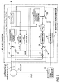
- Fig. 1 is a block diagram showing a reference signal generation circuit according to a first embodiment of the present invention
- Fig. 2 is a block diagram showing a reference signal generation circuit according to a second embodiment of the present invention
- Fig. 3 is a block diagram showing a reference signal generation circuit according to a third embodiment of the present invention
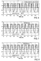
- Fig. 4 is a diagram showing waveforms at a low rotation speed
- Fig. 5 is a diagram showing waveforms at a high rotation speed
- Fig. 6 is a diagram showing rising and falling edges when conventional rising and falling edge detection is applied to the case shown in Fig. 5
- Fig. 7 is a diagram showing the waveform of a reference signal generated from edge detection shown in Fig. 6 in the conventional method
- Fig. 8 is a diagram showing the waveform of a reference signal in the present invention
- Fig. 9 is a block diagram showing a conventional reference signal generation method.
- Fig. 1 shows a reference signal generator 50 according to a first embodiment of the present invention, together with a resolver 20, an excitation signal generator 30, and an angle calculation section 40.
- the resolver 20 is a one-phase-excitation and two-phase-output resolver.
- the resolver 20 receives an excitation signal sin ⁇ t from the excitation signal generator 30.
- the resolver 20 outputs two-phase resolver detection signals sin ⁇ sin( ⁇ t+ ⁇ ) and cos ⁇ sin( ⁇ t+ ⁇ ) to the angle calculation section 40 and also to the reference signal generator 50, where ⁇ indicates the phase difference of the detection signals output from the resolver 20 with respect to the excitation signal sin ⁇ t.
- the angle calculation section 40 and the reference signal generator 50 constitute an angle converter 60.
- the angle calculation section 40 includes a first multiplier 41, a second multiplier 42, a subtractor 43, a synchronous detection circuit 44, a controller 45, a sine ROM 46, and a cosine ROM 47.
- the angle calculation section 40 converts the detection angle ⁇ obtained from the resolver detection signals sin ⁇ sin( ⁇ t+ ⁇ ) and cos ⁇ sin( ⁇ t+ ⁇ ) to a digital output angle ⁇ and outputs it.
- the sine ROM 46 and the cosine ROM 47 store the values of sin ⁇ and cos ⁇ at each angle ⁇ in tables.
- the sine ROM 46 outputs the sine value sin ⁇ at a given digital output angle ⁇ to the multiplier 42.
- the cosine ROM 47 outputs the cosine value cos ⁇ at the given digital output angle ⁇ to the multiplier 41.
- the multiplier 41 multiplies the resolver detection signal sin ⁇ sin( ⁇ t+ ⁇ ) by cos ⁇ and sends the product sin ⁇ sin( ⁇ t+ ⁇ )cos ⁇ to the subtractor 43.
- the multiplier 42 multiplies the resolver detection signal cos ⁇ sin( ⁇ t+ ⁇ ) by sin ⁇ and sends the product cos ⁇ sin( ⁇ t+ ⁇ )sin ⁇ to the subtractor 43.
- the subtractor 43 subtracts the output of the multiplier 42, cos ⁇ sin( ⁇ t+ ⁇ )sin ⁇ , from the output of the multiplier 41, sin ⁇ sin( ⁇ t+ ⁇ )cos ⁇ , and sends the difference, sin( ⁇ - ⁇ )sin( ⁇ t+ ⁇ ), to the synchronous detection circuit 44.
- the controller 45 controls the digital output angle ⁇ so as to make the control deviation sin( ⁇ - ⁇ ) zero. With this operation, the detection angle ⁇ is converted to the digital output angle ⁇ .
- the reference signal generator 50 includes a first multiplier 51, a second multiplier 52, and an adder 53.
- the multiplier 51 multiplies the resolver detection signal sin ⁇ sin( ⁇ t+ ⁇ ) by sin ⁇ obtained from the sine ROM 46 of the angle calculation section 40 and outputs the product, sin ⁇ sin ⁇ sin( ⁇ t+ ⁇ ), to the adder 53.
- the multiplier 52 multiplies the resolver detection signal cos ⁇ sin( ⁇ t+ ⁇ ) by cos ⁇ obtained from the cosine ROM 47 of the angle calculation section 40 and outputs the product, cos ⁇ cos ⁇ sin( ⁇ t+ ⁇ ), to the adder 53.
- the adder 53 adds the output of the multiplier 51, sin ⁇ sin ⁇ sin( ⁇ t + ⁇ ), and the output of the multiplier 52, cos ⁇ cos ⁇ sin( ⁇ t+ ⁇ ), and outputs the following sum.
- cos ⁇ cos ⁇ + sin ⁇ sin ⁇ ⁇ sin ⁇ t + ⁇ cos ⁇ - ⁇ ⁇ sin ⁇ t + ⁇
- the reference signal generator 50 outputs sin( ⁇ t+ ⁇ ), generated in this manner, as the reference signal S R to the synchronous detection circuit 44 of the angle calculation section 40.
- the synchronous detection circuit 44 can perform detection exactly synchronous with the resolver detection signals in terms of the phase ⁇ to obtain sin( ⁇ - ⁇ ) as a synchronous detection output.
- the reference signal S R sin( ⁇ t+ ⁇ ) is generated by the multiplications and additions of sin ⁇ and cos ⁇ obtained from the sine ROM 46 and the cosine ROM 47 of the angle calculation section 40 of a tracking loop type and the two-phase resolver detection signals sin ⁇ sin( ⁇ t+ ⁇ ) and cos ⁇ sin( ⁇ t+ ⁇ )
- the reference signal S R sin( ⁇ t+ ⁇ ) is theoretically generated by calculations, not by extraction from the resolver detection signals with waveform manipulation or at zero crossing timing, the reference signal S R has exactly the same phase as the resolver detection signals.
- Fig. 2 shows a reference signal generator 50' according to another embodiment of the present invention, together with a resolver 20, an excitation signal generator 30, and an angle calculation section 40.
- a resolver 20 an excitation signal generator 30
- an angle calculation section 40 an angle calculation section 40.
- the above described drawback is solved.
- synchronous detection is performed with an excitation signal sin ⁇ t to give priority to tracking.
- synchronous detection is performed with a reference signal S R whose phase is exactly the same as the resolver detection signals.
- the reference signal generator 50' has a tracking loop lock signal generator 54 and a switch 55 in addition to the components of the reference signal generator 50, shown in Fig. 1 .
- the tracking loop signal generator 54 compares the absolute value of a control deviation output from the angle calculation section 40 with a predetermined value and outputs the result.
- the switch 55 is connected to the output of an adder 53 and an excitation signal sin ⁇ t sent from the excitation signal generator 30. Based on the output of the tracking loop lock signal generator 54, the switch 55 switches between the output of the adder 53 and the excitation signal sin ⁇ t. The output of the switch 55 is input to a synchronous detection circuit 44 of the angle calculation section 40 as a reference signal S R .
- a signal indicating whether the tracking loop has achieved tracking is generated by the tracking loop lock signal generator 54 and used as the switching condition of the switch 55.
- the predetermined value to be compared with the absolute value of the control deviation sin( ⁇ - ⁇ ) is, for example, set to 30 degrees.
- is equal to or smaller than 30 degrees.
- the switch 55 outputs the output of the adder 53 as the reference signal S R .
- the switch 55 outputs the excitation signal sin ⁇ t as the reference signal S R .
- the reference signal generator 50' shown in Fig. 2 , even when the tracking loop has not yet achieved tracking in a transition period, such as when
- Fig. 3 shows a reference signal generator 50" according to still another embodiment of the present invention, together with a resolver 20, an excitation signal generator 30, and an angle calculation section 40.
- the reference signal generator 50" includes a first comparator 56, a phase locked loop (hereinafter called PLL) 57, and a second comparator 58, in addition to the components of the reference signal generator 50', shown in Fig. 2 .
- PLL phase locked loop
- a signal sin( ⁇ t+ ⁇ ) output from an adder 53 is converted to a rectangular wave signal by the first comparator 56.
- the rectangular wave signal is used by the PLL 57 to generate a rectangular wave signal having the same phase, and this rectangular wave signal is sent to a switch 55.
- the second comparator 58 converts an excitation signal sin ⁇ t to a rectangular wave signal and sends the rectangular wave signal to the switch 55.
- the resolver detection signals include noise. Therefore, when a method for generating a reference signal from the resolver detection signals is used, it is inevitable that noise causes the reference signal to have a phase fluctuation.
- the rectangular wave signal generated from sin( ⁇ t+ ⁇ ) passes through the PLL 57. Therefore, noise included in the resolver detection signals is prevented from causing phase fluctuation of the reference signal S R , providing a highly noise immune, stable reference signal S R .
- Fig. 4 and Fig. 5 show signal waveforms obtained at a low rotation rate (100 rps) and at a high rotation rate (3,000 rps) with the frequency of an excitation signal being set to 10 kHz.
- the resolver detection signals sin ⁇ sin( ⁇ t + ⁇ ) and cos ⁇ sin( ⁇ t+ ⁇ ) differ only in amplitude from the sin ⁇ t signal, as shown in Fig. 4 . It is understood that the reference signal can be generated from the resolver detection signals.
- the zero crossing points of the resolver detection signals and the zero crossing points of the excitation signal component sin( ⁇ t+ ⁇ ) do not match in timing, as shown in Fig. 5 .
- a reference signal having a uniform phase and duty cycle can be generated, as shown in Fig. 8 even at a high rotation rate (3,000 rps).
Landscapes
- Engineering & Computer Science (AREA)
- Theoretical Computer Science (AREA)
- Transmission And Conversion Of Sensor Element Output (AREA)
- Measurement Of Length, Angles, Or The Like Using Electric Or Magnetic Means (AREA)
Claims (5)
- Circuit (50) de génération de signal de référence destiné à générer un signal de référence (SR) utilisé dans une détection synchrone (44) afin de retirer une composante de signal d'excitation dans une section (40) de calcul d'angle qui convertit un angle de détection θ obtenu à partir de signaux de détection de résolveur à deux phases délivrés en sortie à partir d'un résolveur (20) excité par un signal d'excitation sin ωt, en un angle de sortie numérique Φ, le circuit de génération de signal de référence étant caractérisé en ce qu'il comprend :un premier multiplicateur (51) pour multiplier un premier signal de détection de résolveur sinθsin (ωt + Δω), où Δω indique une différence de phase entre le signal d'excitation et la composante de signal d'excitation, par la valeur sinusoïdale sin Φ de l'angle de sortie numérique Φ obtenu à partir de la section de calcul d'angle ;un deuxième multiplicateur (52) pour multiplier un deuxième signal de détection de résolveur cosθsin (ωt + Δω) par la valeur cosinusoïdale cos Φ de l'angle de sortie numérique Φ obtenu à partir de la section de calcul d'angle ; etun additionneur (53) pour additionner la sortie du premier multiplicateur et la sortie du deuxième multiplicateur pour délivrer en sortie le signal de la somme sin (ωt + Δω) en tant que signal de référence.
- Circuit (54) de génération de signal de référence selon la revendication 1, comprenant en outre :un générateur de signal de verrouillage de boucle de poursuite adapté pour comparer la valeur absolue d'un écart de commande obtenu à partir de la section de calcul d'angle avec une valeur prédéterminée pour délivrer en sortie un résultat de comparaison ; etun commutateur (55) pour commuter entre la sortie sin(ωt + Δω) de l'additionneur et le signal d'excitation sin ωt, sur la base de la sortie du générateur de signal de verrouillage de boucle de poursuite ;dans lequel on commute entre sin (ωt + Δω) et sin ωt sur la base de l'ampleur de l'écart de commande et on les délivre en sortie en tant que signal de référence.
- Circuit de génération de signal de référence selon la revendication 2, comprenant en outre ;un premier comparateur (56) adapté pour mettre la sortie sin (ωt + Δω) de l'additionneur sous forme d'un signal d'onde rectangulaire ;un circuit (57) de synchronisation de phase adapté pour générer un signal d'onde rectangulaire ayant la même phase que la sortie du premier comparateur pour émettre le signal d'onde rectangulaire au commutateur ; etun deuxième comparateur (58) adapté pour mettre le signal d'excitation sin ωt sous forme d'un signal d'onde rectangulaire et pour émettre le signal d'onde rectangulaire au commutateur.
- Convertisseur d'angle comprenant :une section de calcul d'angle adaptée pour convertir un angle de détection θ obtenu à partir de signaux de détection de résolveur à deux phases délivrés en sortie à partir d'un résolveur en un angle de sortie numérique Φ ; etun circuit de génération de signal de référence selon l'une des revendications 1 à 3.
- Appareil de détection d'angle comprenant:un résolveur adapté pour délivrer en sortie des signaux de détection à deux phases ;un convertisseur d'angle selon la revendication 4 ; etun générateur de signal d'excitation adapté pour émettre un signal d'excitation sin ωt au résolveur.
Applications Claiming Priority (1)
| Application Number | Priority Date | Filing Date | Title |
|---|---|---|---|
| JP2007332231A JP4422757B2 (ja) | 2007-12-25 | 2007-12-25 | リファレンス信号生成回路、角度変換器及び角度検出装置 |
Publications (3)
| Publication Number | Publication Date |
|---|---|
| EP2077621A2 EP2077621A2 (fr) | 2009-07-08 |
| EP2077621A3 EP2077621A3 (fr) | 2010-03-10 |
| EP2077621B1 true EP2077621B1 (fr) | 2012-09-26 |
Family
ID=40451301
Family Applications (1)
| Application Number | Title | Priority Date | Filing Date |
|---|---|---|---|
| EP08021616A Active EP2077621B1 (fr) | 2007-12-25 | 2008-12-12 | Circuit de génération de signal de référence, convertisseur d'angle, et appareil de détection d'angle |
Country Status (4)
| Country | Link |
|---|---|
| US (1) | US8004276B2 (fr) |
| EP (1) | EP2077621B1 (fr) |
| JP (1) | JP4422757B2 (fr) |
| CA (1) | CA2646214C (fr) |
Families Citing this family (7)
| Publication number | Priority date | Publication date | Assignee | Title |
|---|---|---|---|---|
| JP2013152204A (ja) * | 2011-01-28 | 2013-08-08 | Nsk Ltd | レゾルバデジタルコンバータマッチング回路、レゾルバ装置、モータ装置及びモータドライブユニット |
| JP5281126B2 (ja) * | 2011-07-15 | 2013-09-04 | 三菱電機株式会社 | レゾルバによる角度検出方法 |
| JP6525846B2 (ja) * | 2015-10-23 | 2019-06-05 | 日本航空電子工業株式会社 | レゾルバ |
| DE102016223938B4 (de) * | 2016-12-01 | 2018-06-14 | Schaeffler Technologies AG & Co. KG | Verfahren zur Demodulation von Signalen eines Sinus-Cosinus-Rotationssensors |
| US10218378B1 (en) * | 2018-08-17 | 2019-02-26 | Robert Bosch Gmbh | Analog converter for motor angle sensor |
| CN114578125A (zh) * | 2022-03-08 | 2022-06-03 | 广汽埃安新能源汽车有限公司 | 旋变过零点检测系统、方法及车辆 |
| CN118168449B (zh) * | 2024-05-13 | 2024-10-18 | 南通汤姆瑞斯工业智能科技有限公司 | 一种电机转角测量系统及方法 |
Family Cites Families (2)
| Publication number | Priority date | Publication date | Assignee | Title |
|---|---|---|---|---|
| JP3442316B2 (ja) | 1999-06-11 | 2003-09-02 | 多摩川精機株式会社 | アナログ信号のディジタル変換方法 |
| JP4627746B2 (ja) * | 2005-07-19 | 2011-02-09 | 日立オートモティブシステムズ株式会社 | 位相検出回路及びこれを用いたレゾルバ/デジタル変換器並びに制御システム |
-
2007
- 2007-12-25 JP JP2007332231A patent/JP4422757B2/ja active Active
-
2008
- 2008-12-11 CA CA2646214A patent/CA2646214C/fr active Active
- 2008-12-12 EP EP08021616A patent/EP2077621B1/fr active Active
- 2008-12-19 US US12/317,094 patent/US8004276B2/en active Active
Also Published As
| Publication number | Publication date |
|---|---|
| EP2077621A2 (fr) | 2009-07-08 |
| US8004276B2 (en) | 2011-08-23 |
| CA2646214C (fr) | 2012-04-10 |
| JP2009156609A (ja) | 2009-07-16 |
| EP2077621A3 (fr) | 2010-03-10 |
| US20090160436A1 (en) | 2009-06-25 |
| JP4422757B2 (ja) | 2010-02-24 |
| CA2646214A1 (fr) | 2009-06-25 |
Similar Documents
| Publication | Publication Date | Title |
|---|---|---|
| EP2077621B1 (fr) | Circuit de génération de signal de référence, convertisseur d'angle, et appareil de détection d'angle | |
| US7859254B2 (en) | Clock generation circuit, analog-digital angle converter using the same, and angle detection apparatus | |
| EP1968197B1 (fr) | Convertisseur d'angle numérique de type à boucle de poursuite et appareil de conversion d'angle en valeur numérique | |
| US8188896B2 (en) | Digital converter for processing resolver signal | |
| JP2011033602A (ja) | レゾルバ/デジタル変換装置およびレゾルバ/デジタル変換方法 | |
| JP2004064515A (ja) | 周期性信号制御装置及び周波数検出装置 | |
| KR101012740B1 (ko) | 레졸버 디지털 변환장치 및 이를 이용한 위치 측정 장치 | |
| JP6809707B2 (ja) | アナログ信号をディジタル信号に変換する方法 | |
| JP2006017659A (ja) | アナログ信号のデジタル変換方法 | |
| US8924179B2 (en) | Assembly and method for determining an angular position | |
| JP2012058007A (ja) | アナログ信号のデジタル変換方法 | |
| EP2003779B1 (fr) | Composant de boucle pll | |
| JP2018066640A (ja) | アナログ信号をディジタル信号に変換する方法および装置 | |
| JP3958255B2 (ja) | 発電機における位相同期検出回路 | |
| JP5361658B2 (ja) | レゾルバデジタルコンバータ | |
| US11397418B2 (en) | Methods and apparatus for an encoder | |
| JP4710634B2 (ja) | モータ制御装置 | |
| JP5798844B2 (ja) | ディジタル発振器 | |
| JPH07183813A (ja) | シンクロ・ディジタル変換装置 | |
| JP2020008512A (ja) | R/d変換器 | |
| JPH04140926A (ja) | シンクロ・ディジタル変換装置 | |
| JPH0380246B2 (fr) |
Legal Events
| Date | Code | Title | Description |
|---|---|---|---|
| PUAI | Public reference made under article 153(3) epc to a published international application that has entered the european phase |
Free format text: ORIGINAL CODE: 0009012 |
|
| 17P | Request for examination filed |
Effective date: 20081218 |
|
| AK | Designated contracting states |
Kind code of ref document: A2 Designated state(s): AT BE BG CH CY CZ DE DK EE ES FI FR GB GR HR HU IE IS IT LI LT LU LV MC MT NL NO PL PT RO SE SI SK TR |
|
| AX | Request for extension of the european patent |
Extension state: AL BA MK RS |
|
| PUAL | Search report despatched |
Free format text: ORIGINAL CODE: 0009013 |
|
| AK | Designated contracting states |
Kind code of ref document: A3 Designated state(s): AT BE BG CH CY CZ DE DK EE ES FI FR GB GR HR HU IE IS IT LI LT LU LV MC MT NL NO PL PT RO SE SI SK TR |
|
| AX | Request for extension of the european patent |
Extension state: AL BA MK RS |
|
| AKX | Designation fees paid |
Designated state(s): DE FR GB |
|
| REG | Reference to a national code |
Ref country code: DE Ref legal event code: R079 Ref document number: 602008018941 Country of ref document: DE Free format text: PREVIOUS MAIN CLASS: H03M0001480000 Ipc: H03M0001080000 |
|
| GRAP | Despatch of communication of intention to grant a patent |
Free format text: ORIGINAL CODE: EPIDOSNIGR1 |
|
| RIC1 | Information provided on ipc code assigned before grant |
Ipc: H03M 1/08 20060101AFI20120328BHEP Ipc: H03M 1/48 20060101ALN20120328BHEP |
|
| GRAS | Grant fee paid |
Free format text: ORIGINAL CODE: EPIDOSNIGR3 |
|
| GRAA | (expected) grant |
Free format text: ORIGINAL CODE: 0009210 |
|
| AK | Designated contracting states |
Kind code of ref document: B1 Designated state(s): DE FR GB |
|
| REG | Reference to a national code |
Ref country code: GB Ref legal event code: FG4D |
|
| REG | Reference to a national code |
Ref country code: DE Ref legal event code: R096 Ref document number: 602008018941 Country of ref document: DE Effective date: 20121122 |
|
| PLBE | No opposition filed within time limit |
Free format text: ORIGINAL CODE: 0009261 |
|
| STAA | Information on the status of an ep patent application or granted ep patent |
Free format text: STATUS: NO OPPOSITION FILED WITHIN TIME LIMIT |
|
| 26N | No opposition filed |
Effective date: 20130627 |
|
| REG | Reference to a national code |
Ref country code: DE Ref legal event code: R097 Ref document number: 602008018941 Country of ref document: DE Effective date: 20130627 |
|
| REG | Reference to a national code |
Ref country code: FR Ref legal event code: PLFP Year of fee payment: 8 |
|
| REG | Reference to a national code |
Ref country code: FR Ref legal event code: PLFP Year of fee payment: 9 |
|
| REG | Reference to a national code |
Ref country code: FR Ref legal event code: PLFP Year of fee payment: 10 |
|
| PGFP | Annual fee paid to national office [announced via postgrant information from national office to epo] |
Ref country code: DE Payment date: 20251028 Year of fee payment: 18 |
|
| PGFP | Annual fee paid to national office [announced via postgrant information from national office to epo] |
Ref country code: GB Payment date: 20251030 Year of fee payment: 18 |
|
| PGFP | Annual fee paid to national office [announced via postgrant information from national office to epo] |
Ref country code: FR Payment date: 20251117 Year of fee payment: 18 |