EP2079281A2 - Bidirektionale Leuchtdiodentreiberschaltung in bidirektionaler geteilter Stromresonanz - Google Patents
Bidirektionale Leuchtdiodentreiberschaltung in bidirektionaler geteilter Stromresonanz Download PDFInfo
- Publication number
- EP2079281A2 EP2079281A2 EP09250088A EP09250088A EP2079281A2 EP 2079281 A2 EP2079281 A2 EP 2079281A2 EP 09250088 A EP09250088 A EP 09250088A EP 09250088 A EP09250088 A EP 09250088A EP 2079281 A2 EP2079281 A2 EP 2079281A2
- Authority
- EP
- European Patent Office
- Prior art keywords
- light emitting
- impedance
- directional
- emitting diode
- power
- Prior art date
- Legal status (The legal status is an assumption and is not a legal conclusion. Google has not performed a legal analysis and makes no representation as to the accuracy of the status listed.)
- Withdrawn
Links
Images




Classifications
-
- H—ELECTRICITY
- H05—ELECTRIC TECHNIQUES NOT OTHERWISE PROVIDED FOR
- H05B—ELECTRIC HEATING; ELECTRIC LIGHT SOURCES NOT OTHERWISE PROVIDED FOR; CIRCUIT ARRANGEMENTS FOR ELECTRIC LIGHT SOURCES, IN GENERAL
- H05B45/00—Circuit arrangements for operating light-emitting diodes [LED]
- H05B45/40—Details of LED load circuits
- H05B45/44—Details of LED load circuits with an active control inside an LED matrix
Definitions
- the bi-directional light emitting diode drive circuit in bi-directional divided power impedance is disclosed by that an AC power or a periodically alternated polarity power is used as the power source to supply to the resistive impedance components, or inductive impedance components, or capacitive impedance components in mutual series connection, whereby the power source voltage is divided.
- the said divided power across the two ends of the first impedance and the second impedance is used to drive a bi-directional conducting light emitting diode, or to drive at least two bi-directional conducting light emitting diode sets which are respectively parallel connected across the two ends of the first impedance and the second impedance.
- the conventional light emitting diode drive circuit using AC or DC power source is usually series connected with current limit resistors as the impedance to limit the current to the light emitting diode, whereof the voltage drop of the series connected resistive impedance always result in waste of power and accumulation of heat which are the imperfections.
- the invention is that the first impedance is constituted by capacitive impedance components, inductive impedance components, or resistive impedance components and a second impedance is constituted by capacitive impedance components, inductive impedance components, or resistive impedance components; whereof, the first impedance and the second impedance are in series connection to receive the following:
- the divided power is formed at the first impedance and the second impedance through the input of above said powers, whereby the first light emitting diode and the second light emitting diode are parallel connected in reverse polarities to constitute a bi-directional conducting light emitting diode set which is parallel connected across the two ends of the second impedance and is driven by the divided power across the two ends of the second impedance to emit light.
- C100, C102, C200 Capacitor CR100, CR101, CR102, CR201, CR202: Diode ESD101, ESD102: Charge/discharge device I100, I103, I104, I200: Inductive impedance component IT200: Separating type transformer L100: Bi-directional conducting light emitting diode set LED 101: First light emitting diode LED 102: Second light emitting diode R101, R102: Discharge resistor R100, R103, R104: Current limit resistor ST200: Self-coupled transformer U100: Bi-directional light emitting diode (LED) drive circuit W0: Self-coupled voltage change winding W1: Primary side winding W2: Secondary side winding Z101: First impedance Z102: Second impedance ZD101, ZD 102: Zener diode 300: Bi-directional power modulator of series connection type 400: Bi-directional power modulator of parallel connection type 500: Impedance component 600: Switching device 4000: DC to AC Inverter
- the bi-directional light emitting diode drive circuit in bi-directional divided power impedance is disclosed by that at least one first impedance is constituted capacitive impedance components, inductive impedance components, or resistive impedance components and at least one second impedance is constituted by capacitive impedance components, inductive impedance components, or resistive impedance components; at least one first light emitting diode and at least one second light emitting diode are in parallel connection of reverse polarities thereby to constitute at least one bi-directional conducting light emitting diode set which is parallel connected across the two ends of at least one second impedance, whereof the two ends of at least one first impedance and at least one second impedance in mutual series connection is provided to receive the following:
- the divided power is formed at the first impedance and the second impedance in series connection through the above said powers to drive at least one bi-directional conducting light emitting diode set, or to drive at least two bi-directional conducting light emitting diode sets which are respectively parallel connected across the two ends of the first impedance and the two ends of the second impedance, thereby to constitute the bi-directional light emitting diode drive circuit in bi-directional divided power impedance.
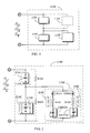
- the first impedance (Z101), the second impedance (Z102) and the bi-directional conducting light emitting diode set (L100) are connected according to the aforesaid circuit structure to constitute the bi-directional light emitting diode drive circuit (U100) and through the current distribution effect formed by the parallel connection of the bi-directional conducting light emitting diode set (L100) and the second impedance (Z102), the voltage variation rate across the two ends of the bi-directional conducting light emitting diode set (L100) corresponding to power source voltage variation can be reduced;
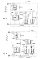
- the bi-directional light emitting diode drive circuit in bi-directional divided power impedance, whereof selections of the first light emitting diode (LED101) and the second light emitting diode (LED 102) which constitute the bi-directional conducting light emitting diode set (L100) in the bi-directional light emitting diode drive circuit (U100) include the following:
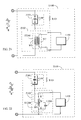
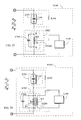
- Fig. 3 is a circuit example schematic diagram of the invention illustrating that the bi-directional conducting light emitting diode set is constituted by a first light emitting diode and a diode in parallel connection of reverse polarities.
- the bi-directional light emitting diode drive circuit can be as shown in Figs. 1, 2 and 3 when it is in actual applications the following auxiliary circuit components can be optionally selected as needed to be installed or not installed while the quantity of the installation can be constituted by one or more than one, whereof in case more than one are selected, they can be selected based on circuit function requirements to be in series connection or parallel connection or series and parallel connection in corresponding polarities, whereof the optionally selected auxiliary circuit components include:
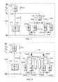
- a zener diode can be further parallel connected across the two ends of the first light emitting diode (LED101) and the second light emitting diode (LED102) in the bi-directional conducting light emitting diode set (L100) of the bi-directional light emitting diode drive circuit (U100) as shown in circuit examples of Figs. 5, 6 , or the zener diode is first series connected with at least one diode to produce a zener voltage function, then parallel connected across the two ends of the first light emitting diode (LED 101) or of the second light emitting diode (LED 102);
- Fig. 5 is a circuit example schematic diagram illustrating that the bi-directional conducting light emitting diode set in the circuit of Fig. 2 is further installed with a zener diode.
- Fig. 6 is a circuit example schematic diagram illustrating that the bi-directional conducting light emitting diode set in the circuit of Fig. 3 is further installed with a zener diode;
- Fig. 7 is a circuit example schematic diagram illustrating that the bi-directional conducting light emitting diode set in the circuit of Fig. 4 is further installed with a zener diode; whereof it is constituted by the following:
- the said zener diode (ZD102) can be optionally series connected with a diode (CR202) as needed, whereof the advantages are 1) the zener diode (ZD102) can be protected from reverse current; 2) both diode (CR202) and zener diode (ZD102) have temperature compensation effects.
- the zener diode is constituted by the following:
- the aforesaid charge/discharge devices (ESD101), (ESD102) can be constituted by the conventional charging and discharging
- the bi-directional light emitting diode drive circuit in bi-directional divided power impedance can be further optionally installed with a charge/discharge device as needed, whereof it includes:
- a charge/discharge device (ESD101) or a charge/discharge device (ESD102) can be further installed across the two ends of the bi-directional conducting light emitting diode set (L100) in the bi-directional light emitting diode drive circuit (U100) for random charging/discharging, thereby besides of stabilizing the lighting stabilities of the first light emitting diode (LED101) and the second light emitting diode (LED102) of the bi-directional conducting light emitting diode set (L100), the charge/discharge device can provide its saving power during a power off to drive at least one of the first light emitting diode (LED101) or the second light emitting diode (LED 102) to continue emitting light;
- the aforesaid charge/discharge devices (ESD101), (ESD102) can be constituted by the conventional charging and discharging batteries, or super-capacitors or capacitors, etc.
- the first impedance (Z101), the second impedance (Z102) and the bi-directional conducting light emitting diode set (L100) as well as the first light emitting diode (LED101), the second light emitting diode (LED 102) and various aforesaid optional auxiliary circuit components as shown in the circuit examples of Figs. 1 ⁇ 11 are based on application needs, whereof they can be optionally installed or not installed as needed and the installation quantity include constitution by one, wherein if more than one are selected, the corresponding polarity relationship shall be determined based on circuit function requirement to execute series connection, or parallel connection or series and parallel connections; thereof it is constituted as the following:
- active modulating circuit devices can be further optionally combined as needed, whereof the applied circuits are the following:
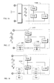
- the bi-directional light emitting diode drive circuit in bi-directional divided power impedance in which the optionally installed inductive impedance component (I200) of the second impedance (Z102) can be further replaced by the power supply side winding of a transformer with inductive effect, whereof the transformer can be a self-coupled transformer (ST200) with self-coupled voltage change winding or a transformer (IT200) with separating type voltage change winding;
- Fig. 19 is a circuit example schematic diagram of the invention illustrating that the inductive impedance component of the second impedance is replaced by the self-coupled voltage change power supply side winding of the self-coupled transformer thereby to constitute a voltage rise, whereof as shown in Fig.
- the self-coupled transformer (ST200) has a self-coupled voltage change winding (W0) with voltage raising function
- the b, c ends of the self-coupled voltage change winding (W0) of the self-coupled transformer (ST200) are the power supply side which replace the inductive impedance component (I200) of the second impedance (Z102), thereby to constitute the second impedance (Z102), whereof the a, c output ends of the self-coupled voltage change winding (W0) of the self-coupled transformer (ST200) are arranged to provide AC power of voltage rise to drive the bi-directional conducting light emitting diode set (L100);
- Fig. 20 is a circuit example schematic diagram of the invention illustrating that the inductive impedance component of the second impedance is replaced by the self-coupled voltage change power supply side winding of the self-coupled transformer thereby to constitute a voltage drop, whereof as shown in Fig.
- the self-coupled transformer (ST200) has a self-coupled voltage change winding (W0) with voltage drop function, in which the b, c ends of the self-coupled voltage change winding (W0) of the self-coupled transformer (ST200) are the power supply side which replace the inductive impedance component (I200) of the second impedance (Z 102), thereby to constitute the second impedance (Z102), whereof the a, c output ends of the self-coupled voltage change winding (W0) of the self-coupled transformer (ST200) are arranged to provide AC power of voltage drop to drive the bi-directional conducting light emitting diode set (L 100);
- Fig. 21 is a circuit example schematic diagram of the invention illustrating that the inductive impedance component of the second impedance is replaced by the primary side winding of the separating type transformer with separating type voltage change winding, whereof as shown in Fig. 21 , the separating type transformer (IT200) is comprised of a primary side winding (W1 and a secondary side winding (W2), in which the primary side winding (W1)and the secondary side winding (W2) are separated, while the primary side winding (W1 constitute the second impedance (Z102), whereof the output voltage of the secondary side winding (W2) of the separating type transformer (IT200) can be optionally selected as needed to provide AC power of voltage rise or voltage drop to drive the bi-directional conducting light emitting diode set (L100).
- the separating type transformer (IT200) is comprised of a primary side winding (W1 and a secondary side winding (W2), in which the primary side winding (W1)and the secondary side winding (W2) are separated,
- the inductive impedance component (I200) of the second impedance (Z102) is replaced by the power supply side winding of the transformer, whereof the secondary side of the separating type transformer (IT200) provides AC power of voltage rise or voltage drop to drive the bi-directional conducting light emitting diode set (L100).
- the bi-directional light emitting diode drive circuit in bi-directional divided power impedance in which the optionally installed inductive impedance component (I200) of the second impedance (Z102) can be further replaced by the power supply side winding of a transformer with inductive effect thereby to constitute the second impedance (Z102) which is parallel connected with the capacitor (C200) to appear parallel resonance, whereof the transformer can be a self-coupled transformer (ST200) with self-coupled voltage change winding or a transformer (IT200) with separating type voltage change winding.
- ST200 self-coupled transformer
- IT200 transformer
- Fig. 22 is a circuit example schematic diagram of the invention illustrating that the self-coupled voltage change power supply side winding of the self-coupled transformer is in parallel resonance with the parallel connected capacitor to constitute a voltage rise, whereof as shown in Fig. 22 , the self-coupled transformer (ST200) has a self-coupled voltage change winding (W0) with voltage raising function, the b, c ends of the self-coupled voltage change winding (W0) of the self-coupled transformer (ST200) is the power supply side which replace the inductive impedance component (I200) of the second impedance (Z102) to be parallel connected with the capacitor (C200), whereof its inherent parallel resonance frequency after parallel connection is the same as frequency of the bi-directional power from power source such as the AC power, or the alternated polarity period of the constant or variable voltage and constant or variable periodically alternated polarity power converted from DC power to produce a parallel resonance status, thereby to constitute the second impedance (Z102), which is series connected with the capacitor (C100
- Fig. 23 is a circuit example schematic diagram of the invention illustrating that the self-coupled voltage change power supply side winding of the self-coupled transformer is in parallel resonance with the parallel connected capacitor to constitute a voltage drop, whereof as shown in Fig. 23 , the self-coupled transformer (ST200) has a self-coupled voltage change winding (W0) with voltage drop function, in which the a, c ends of the self-coupled voltage change winding (W0) of the self-coupled transformer (ST200) are the power supply side which replace the inductive impedance component (I200) of the second impedance (Z102) to be parallel connected with the capacitor (C200), whereof its inherent parallel resonance frequency after parallel connection is the same as frequency of the bi-directional power from power source such as the AC power, or the alternated polarity period of the constant or variable voltage and constant or variable periodically alternated polarity power converted from DC power so as to produce a parallel resonance status, thereby to constitute the second impedance (Z102), which is series connected with the
- Fig. 24 is a circuit example schematic diagram of the invention illustrating that the primary side winding of the separating type transformer with separating type voltage change winding is parallel connected with a capacitor to appear a parallel resonance status; whereof as shown in Fig. 24 , the separating type transformer (IT200) is comprised of a primary side winding (W1) and a secondary side winding (W2), in which the primary side winding (W1) and the secondary side winding (W2) are separated; the primary side winding (W1) is parallel connected with the capacitor (C200), whereof its inherent parallel resonance frequency after parallel connection is the same as frequency of the bi-directional power from power source such as the AC power, or the alternated polarity period of the constant or variable voltage and constant or variable periodically alternated polarity power converted from DC power so as to produce a parallel resonance status, thereby to constitute the second impedance (Z102), which is series connected with the capacitor (C100) of the first impedance (Z101); further, the capacitor (C200) can be optionally parallel connected with the
- the inductive impedance component (I200) of the second impedance (Z102) is replaced by the power supply side winding of the transformer and is parallel connected with the capacitor (C200) to appear parallel resonance, thereby to constitute the second impedance while the secondary side of the separating type transformer (IT200) provides AC power of voltage rise or voltage drop to drive the bi-directional conducting light emitting diode set (L 100).
- Color of the individual light emitting diodes (LED101), (LED 102) of the bi-directional conducting light emitting diode set (L100) in the bi-directional light emitting diode drive circuit (U100) of the bi-directional light emitting diode drive circuit in bi-directional divided power impedance can be optionally selected to be constituted by one or more than one colors.
- the relationships of location arrangement between the individual light emitting diodes (LED101) of the bi-directional conducting light emitting diode set (L100) in the bi-directional light emitting diode drive circuit (U100) of the bi-directional light emitting diode drive circuit in bi-directional divided power impedance include the following: 1) sequentially linear arrangement; 2) sequentially distributed in a plane; 3) crisscross-linear arrangement; 4) crisscross distribution in a plane; 5) arrangement based on particular geometric positions in a plane; 6) arrangement based on 3D geometric position.
- the bi-directional light emitting diode drive circuit in bi-directional divided power impedance in which the embodiments of its bi-directional light emitting diode drive circuit (U100) are constituted by circuit components which include: 1) It is constituted by individual circuit components which are inter-connected; 2) At least two circuit components are combined to at least two partial functioning units which are further inter-connected; 3) All components are integrated together to one structure.
- progressive performances of power saving, low heat loss and low cost can be provided by the bi-directional light emitting diode drive circuit in bi-directional divided power impedance through the charging/discharging by the uni-polar capacitor to drive light emitting diode.
- the present invention provides a bi-directional light emitting diode drive circuit in bi-directional divided power impedance, which uses the capacitive, or inductive, or resistive impedance components to constituted at least one first impedance, and uses the capacitive, or inductive, or resistive impedance components to constituted at least one second impedance, as well as uses at least one first light emitting diode and at least one second light emitting diode in parallel connection of reverse polarities to constitute at least one bi-directional conducting light emitting diode set which is parallel connected across the two ends of at least one second impedance; the two ends of at least one first impedance and at least one second impedance in mutual series connection is provided to receive the following:
- the divided power is formed at the first impedance and the second impedance in series connection through the above said powers to drive at least one bi-directional conducting light emitting diode set, or to drive at least two bi-directional conducting light emitting diode sets which are respectively parallel connected across the two ends of the first impedance and the two ends of the second impedance, thereby to constitute the bi-directional light emitting diode drive circuit in bi-directional divided power impedance; whereof it is comprised of that:
- the first light emitting diode (LED101) may be installed with a charge/discharge device (ESD101), or the second light emitting diode (LED 102) can be installed with a charge/discharge device (ESD102), whereof the charge/discharge device (ESD101) and the charge/discharge device (ESD102) have the random charging or discharging characteristics which can stabilize the lighting stability of the first light emitting diode (LED101) and the second light emitting diode (LED 102), whereby to reduce their lighting pulsations; the aforesaid charge/discharge devices (ESD 101), (ESD 102) can be constituted by the conventional charging and discharging batteries, or super-capacitors or capacitors.
- the application circuit with additionally installed the charge/discharge device may include:
- the bi-directional light emitting diode drive circuit in bi-directional divided power impedance, whereof in its bi-directional light emitting diode drive circuit (U100), a charge/discharge device (ESD 101) can be parallel connected across the two ends of the current limit resistor (R103) and the first light emitting diode (LED101) in series connection;
- ESD 101 charge/discharge device
- ESD102 charge/discharge device
- R104 current limit resistor
- LED 102 second light emitting diode
- the aforesaid charge/discharge devices (ESD101), (ESD102) can be constituted by the conventional charging and discharging batteries, or super-capacitors or capacitors.
- a charge/discharge device (ESD101) or a charge/discharge device (ESD102) may further be installed across the two ends of the bi-directional conducting light emitting diode set (L100) in the bi-directional light emitting diode drive circuit (U100) for random charging/discharging, thereby besides of stabilizing the lighting stabilities of the first light emitting diode (LED101) and the second light emitting diode (LED 102) of the bi-directional conducting light emitting diode set (L100), the charge/discharge device can provide its saving power during a power off to drive at least one of the first light emitting diode (LED101)or the second light emitting diode (LED 102) to continue emitting light;
- ESD101 charge/discharge devices
- ESD102 charge/discharge devices
- a diode (CR101) of forward polarity series connection can be optionally installed as needed to prevent reverse voltage from damaging the uni-polar charge/discharge device
- a diode (CR102) of forward polarity series connection can be optionally installed as needed to prevent reverse voltage from damaging the uni-polar charge/discharge device
- the aforesaid charge/discharge devices (ESD101), (ESD102) can be constituted by the conventional charging and discharging batteries, or super-capacitors or capacitors.
- a diode (CR101) may be parallel connected with at least one first light emitting diode (LED 101) in opposite polarities, and a diode (CR102) may be parallel connected with at least one second light emitting diode (LED 102) in opposite polarities, whereof the two are further reversely series connected to constitute a bi-directional conducting light emitting diode set.
- the bi-directional light emitting diode drive circuit (U 100) may be optionally installed with one bi-directional conducting light emitting diode set (L100) or with more than one bi-directional conducting light emitting diode sets (L100) in series connection, parallel connection or series and parallel connection, whereof if one set or more than one sets are selected to be installed, they can be jointly driven by the divided power of the same second impedance (Z102) or driven individually by the corresponding divided power at each of the multiple second impedances (Z102) which are in series connection or parallel connection.
- the peak of light emitting forward voltage can be correspondingly selected based on the duty cycle of current conduction as long as the principle of that the peak of light emitting forward voltage does not damage the light emitting diode is followed.
- the charge/discharge device is not installed, then based on the value and wave shape of the aforesaid light emitting forward voltage, the corresponding current value and wave shape from the forward voltage vs. forward current ratio are produced; however the peak of light emitting forward current shall follow the principle not to damage the light emitting diode (LED 101) or (LED 102).
- the drive circuit may be series connected to the bi-directional power modulator of series connection type, whereof the bi-directional power modulator of series connection type is constituted by the following:
- the optionally installed inductive impedance component (I200) of the second impedance (Z102) may be further replaced by the power supply side winding of a transformer with inductive effect, whereof the self-coupled transformer (ST200) has a self-coupled voltage change winding (W0) with voltage raising function, the b, c ends of the self-coupled voltage change winding (W0) of the self-coupled transformer (ST200) are the power supply side which replace the inductive impedance component (I200) of the second impedance (Z102), thereby to constitute the second impedance (Z102), whereof the a, c output ends of the self-coupled voltage change winding (W0) of the self-coupled transformer (ST200) are arranged to provide AC power of voltage rise to drive the bi-directional conducting light emitting diode set (L100).
- the self-coupled transformer (ST200) has a self-coupled voltage change winding (W0) with voltage raising function
- the optionally installed inductive impedance component (I200) of the second impedance (Z102) may be further replaced by the power supply side winding of a transformer with inductive effect, whereof the self-coupled transformer (ST200) has a self-coupled voltage change winding (W0) with voltage drop function, in which the b, c ends of the self-coupled voltage change winding (W0) of the self-coupled transformer (ST200) are the power supply side which replace the inductive impedance component (I200) of the second impedance (Z 102), thereby to constitute the second impedance (Z102), whereof the a, c output ends of the self-coupled voltage change winding (W0) of the self-coupled transformer (ST200) are arranged to provide AC power of voltage drop to drive the bi-directional conducting light emitting diode set (L100).
- the self-coupled transformer (ST200) has a self-coupled voltage change winding (W0) with voltage drop function, in which the b,
- the optionally installed inductive impedance component (I200) of the second impedance (Z102) may be further replaced by the power supply side winding of a transformer with inductive effect, whereof the separating type transformer (IT200) is comprised of a primary side winding (W1) and a secondary side winding (W2), in which the primary side winding (W1) and the secondary side winding (W2) are separated, while the primary side winding (W1) constitute the second impedance (Z102), whereof the output voltage of the secondary side winding (W2) of the separating type transformer (IT200) can be optionally selected as needed to provide AC power of voltage rise or voltage drop to drive the bi-directional conducting light emitting diode set (L100);
- the inductive impedance component (I200) of the second impedance (Z102) is replaced by the power supply side winding of the transformer, whereof the secondary side of the separating type transformer (IT200) provides AC power of voltage rise or voltage drop to drive the bi-directional conducting light emitting diode set (L100).
- the optionally installed inductive impedance component (I200) of the second impedance (Z102) may be further replaced by the power supply side winding of a transformer with inductive effect, whereof the self-coupled transformer (ST200) has a self-coupled voltage change winding (W0) with voltage raising function, the b, c ends of the self-coupled voltage change winding (W0) of the self-coupled transformer (ST200) is the power supply side which replace the inductive impedance component (I200) of the second impedance (Z102) to be parallel connected with the capacitor (C200), whereof its inherent parallel resonance frequency after parallel connection is the same as frequency of the bi-directional power from power source such as the AC power, or the alternated polarity period of the constant or variable voltage and constant or variable periodically alternated polarity power converted from DC power to produce a parallel resonance status, thereby to constitute the second impedance (Z102), which is series connected with the capacitor (C100) of the first impedance (Z101); further, the capacitor (C
- the optionally installed inductive impedance component (I200) of the second impedance (Z102) may be further replaced by the power supply side winding of a transformer with inductive effect, whereof the self-coupled transformer (ST200) has a self-coupled voltage change winding (W0) with voltage drop function, in which the a, c ends of the self-coupled voltage change winding (W0) of the self-coupled transformer (ST200) are the power supply side which replace the inductive impedance component (I200) of the second impedance (Z 102) to be parallel connected with the capacitor (C200), whereof its inherent parallel resonance frequency after parallel connection is the same as frequency of the bi-directional power from power source such as the AC power, or the alternated polarity period of the constant or variable voltage and constant or variable periodically alternated polarity power converted from DC power so as to produce a parallel resonance status, thereby to constitute the second impedance (Z102), which is series connected with the capacitor (C100) of the first impedance (Z101), further,
- the optionally installed inductive impedance component (I200) of the second impedance (Z102) may be further replaced by the power supply side winding of a transformer with inductive effect, whereof the separating type transformer (IT200) is comprised of a primary side winding (W1) and a secondary side winding (W2), in which the primary side winding (W1) and the secondary side winding (W2) are separated; the primary side winding (W1) is parallel connected with the capacitor (C200), whereof its inherent parallel resonance frequency after parallel connection is the same as frequency of the bi-directional power from power source such as the AC power, or the alternated polarity period of the constant or variable voltage and constant or variable periodically alternated polarity power converted from DC power so as to produce a parallel resonance status, thereby to constitute the second impedance (Z102), which is series connected with the capacitor (C100) of the first impedance (Z101); further, the capacitor (C200) can be optionally parallel connected with the a, c taps or b, c taps of
- the inductive impedance component (I200) of the second impedance (Z102) is replaced by the power supply side winding of the transformer and is parallel connected with the capacitor (C200) to appear parallel resonance, thereby to constitute the second impedance while the secondary side of the separating type transformer (IT200) provides AC power of voltage rise or voltage drop to drive the bi-directional conducting light emitting diode set (L100).
Landscapes
- Led Devices (AREA)
- Circuit Arrangement For Electric Light Sources In General (AREA)
Applications Claiming Priority (1)
| Application Number | Priority Date | Filing Date | Title |
|---|---|---|---|
| US2083608P | 2008-01-14 | 2008-01-14 |
Publications (2)
| Publication Number | Publication Date |
|---|---|
| EP2079281A2 true EP2079281A2 (de) | 2009-07-15 |
| EP2079281A3 EP2079281A3 (de) | 2011-03-30 |
Family
ID=40651818
Family Applications (1)
| Application Number | Title | Priority Date | Filing Date |
|---|---|---|---|
| EP09250088A Withdrawn EP2079281A3 (de) | 2008-01-14 | 2009-01-14 | Bidirektionale Leuchtdiodentreiberschaltung in bidirektionaler geteilter Stromresonanz |
Country Status (6)
| Country | Link |
|---|---|
| US (1) | US8063571B2 (de) |
| EP (1) | EP2079281A3 (de) |
| JP (1) | JP2009170919A (de) |
| CN (2) | CN101489339B (de) |
| CA (1) | CA2649547A1 (de) |
| TW (1) | TWI450641B (de) |
Cited By (2)
| Publication number | Priority date | Publication date | Assignee | Title |
|---|---|---|---|---|
| EP2418917A1 (de) * | 2009-08-27 | 2012-02-15 | Tai-Her Yang | LED des Typs mit umschaltbarer Polarität und Antriebsschaltung |
| EP2343953A3 (de) * | 2009-12-29 | 2014-11-05 | Tai-Her Yang | LED-Vorrichtung mit Spannungsbegrenzung und Verpolungsschutz |
Families Citing this family (10)
| Publication number | Priority date | Publication date | Assignee | Title |
|---|---|---|---|---|
| CN101489339B (zh) * | 2008-01-14 | 2014-07-02 | 杨泰和 | 双向电能阻抗分压的led双向驱动电路 |
| TWI508630B (zh) * | 2008-03-07 | 2015-11-11 | Tai Her Yang | 雙極性充放電之led驅動電路 |
| WO2011093395A1 (ja) * | 2010-01-29 | 2011-08-04 | 三菱化学株式会社 | 白色led発光デバイスの調光装置,及び照明システム |
| JP5740115B2 (ja) * | 2010-08-24 | 2015-06-24 | 楊 泰和 | Led回路 |
| US20130106305A1 (en) * | 2011-02-14 | 2013-05-02 | Bradford K. Whitaker | Light emitting apparatus and method of manufacturing and using the same |
| TW201310883A (zh) * | 2011-08-17 | 2013-03-01 | Memchip Technology Co Ltd | 昇壓電路 |
| JP5602781B2 (ja) * | 2012-03-30 | 2014-10-08 | 株式会社 ヘイワ | Led素子の駆動方法及び駆動用電源装置 |
| JP6047195B2 (ja) * | 2015-04-24 | 2016-12-21 | 楊 泰和 | Led回路 |
| WO2022174923A1 (en) * | 2021-02-21 | 2022-08-25 | Renton Durante | Direct-current dual polarity, light-emitting led circuit |
| TWI875335B (zh) * | 2023-11-24 | 2025-03-01 | 矽誠科技股份有限公司 | 具有並聯定序功能之發光二極體電路、發光二極體燈、發光二極體燈串 |
Family Cites Families (7)
| Publication number | Priority date | Publication date | Assignee | Title |
|---|---|---|---|---|
| AU4850099A (en) * | 1999-06-29 | 2001-01-31 | Welles Reymond | Ac powered led circuits for traffic signal displays |
| US6411045B1 (en) * | 2000-12-14 | 2002-06-25 | General Electric Company | Light emitting diode power supply |
| US6628085B2 (en) * | 2001-01-17 | 2003-09-30 | Tai-Her Yang | Limit voltage circuit using light emitting diodes as thermal-loss reducing impedances, especially for matching a saturation voltage of rechargeable cells during charging |
| US7164237B2 (en) * | 2002-11-21 | 2007-01-16 | Koninklijke Philips Electronics N.V. | Circuit arrangement for operating discharge lamps |
| KR101236238B1 (ko) * | 2006-03-15 | 2013-02-22 | 엘지디스플레이 주식회사 | 엘이디 백라이트 구동회로 |
| EP1845755A3 (de) * | 2006-04-10 | 2014-04-02 | EMD Technologies, Inc. | Beleuchtungssysteme |
| CN101489339B (zh) * | 2008-01-14 | 2014-07-02 | 杨泰和 | 双向电能阻抗分压的led双向驱动电路 |
-
2009
- 2009-01-09 CN CN200910001460.5A patent/CN101489339B/zh not_active Expired - Fee Related
- 2009-01-09 CN CNU2009200019479U patent/CN201369848Y/zh not_active Expired - Lifetime
- 2009-01-12 US US12/351,927 patent/US8063571B2/en not_active Expired - Fee Related
- 2009-01-13 TW TW098101071A patent/TWI450641B/zh not_active IP Right Cessation
- 2009-01-13 CA CA002649547A patent/CA2649547A1/en not_active Abandoned
- 2009-01-14 EP EP09250088A patent/EP2079281A3/de not_active Withdrawn
- 2009-01-14 JP JP2009005362A patent/JP2009170919A/ja active Pending
Cited By (2)
| Publication number | Priority date | Publication date | Assignee | Title |
|---|---|---|---|---|
| EP2418917A1 (de) * | 2009-08-27 | 2012-02-15 | Tai-Her Yang | LED des Typs mit umschaltbarer Polarität und Antriebsschaltung |
| EP2343953A3 (de) * | 2009-12-29 | 2014-11-05 | Tai-Her Yang | LED-Vorrichtung mit Spannungsbegrenzung und Verpolungsschutz |
Also Published As
| Publication number | Publication date |
|---|---|
| CN101489339A (zh) | 2009-07-22 |
| TWI450641B (zh) | 2014-08-21 |
| US20090179579A1 (en) | 2009-07-16 |
| EP2079281A3 (de) | 2011-03-30 |
| TW200932054A (en) | 2009-07-16 |
| CN101489339B (zh) | 2014-07-02 |
| CN201369848Y (zh) | 2009-12-23 |
| US8063571B2 (en) | 2011-11-22 |
| JP2009170919A (ja) | 2009-07-30 |
| CA2649547A1 (en) | 2009-07-14 |
Similar Documents
| Publication | Publication Date | Title |
|---|---|---|
| EP2079281A2 (de) | Bidirektionale Leuchtdiodentreiberschaltung in bidirektionaler geteilter Stromresonanz | |
| EP2079279A2 (de) | Bidirektionale Leuchtidodenansteuerung in Parallelresonanz mit bidirektionaler Leistung | |
| EP2079280A2 (de) | Bidirektionale Leuchtdiodentreiberschaltung in Impulsstromresonanz | |
| CA2650164C (en) | Bipolar (dis)charging led drive method and circuit thereof | |
| EP2079278A2 (de) | Unidirektionale Leuchtdiodentreiberschaltung in bidirektionaler paralleler Stromrezonanz | |
| EP2079283A2 (de) | Bidirektionale Leuchtdiodentreiberschaltung in Impulsstrom-Nichtresonanz | |
| EP2099259A1 (de) | Einpoliges Ent/Ladungs-Ansteuerungsverfahren für LEDs und die dazugehörige Schaltung | |
| CA2649545C (en) | Uni-directional light emitting diode drive circuit in bi-directional divided power impedance | |
| US8049428B2 (en) | Uni-directional light emitting diode drive circuit in pulsed power series resonance | |
| US8054007B2 (en) | Bi-directional light emitting diode drive circuit in bi-directional power series resonance | |
| US8058814B2 (en) | Bi-directional light emitting diode drive circuit in pulsed power series resonance | |
| EP2079277A2 (de) | Unidirektionale Leuchtdiodentreiberschaltung in Impulsstromresonanz | |
| EP2079284A2 (de) | Unidirektionale Leuchtdiodentreiberschaltung in Impulsstrom-Nichtresonanz | |
| US8164271B2 (en) | Uni-directional light emitting diode drive circuit in bi-directional power series resonance | |
| KR20100107690A (ko) | 양방향 전기에너지 병렬공진의 양방향 발광다이오드 구동회로 |
Legal Events
| Date | Code | Title | Description |
|---|---|---|---|
| PUAI | Public reference made under article 153(3) epc to a published international application that has entered the european phase |
Free format text: ORIGINAL CODE: 0009012 |
|
| AK | Designated contracting states |
Kind code of ref document: A2 Designated state(s): AT BE BG CH CY CZ DE DK EE ES FI FR GB GR HR HU IE IS IT LI LT LU LV MC MK MT NL NO PL PT RO SE SI SK TR |
|
| AX | Request for extension of the european patent |
Extension state: AL BA RS |
|
| PUAL | Search report despatched |
Free format text: ORIGINAL CODE: 0009013 |
|
| AK | Designated contracting states |
Kind code of ref document: A3 Designated state(s): AT BE BG CH CY CZ DE DK EE ES FI FR GB GR HR HU IE IS IT LI LT LU LV MC MK MT NL NO PL PT RO SE SI SK TR |
|
| AX | Request for extension of the european patent |
Extension state: AL BA RS |
|
| AKY | No designation fees paid | ||
| REG | Reference to a national code |
Ref country code: DE Ref legal event code: R108 Effective date: 20111207 |
|
| STAA | Information on the status of an ep patent application or granted ep patent |
Free format text: STATUS: THE APPLICATION IS DEEMED TO BE WITHDRAWN |
|
| 18D | Application deemed to be withdrawn |
Effective date: 20111001 |