EP2080229B1 - Dispositifs photovoltaïques comprenant un contact métallique contenant de l'azote - Google Patents
Dispositifs photovoltaïques comprenant un contact métallique contenant de l'azote Download PDFInfo
- Publication number
- EP2080229B1 EP2080229B1 EP07844909.7A EP07844909A EP2080229B1 EP 2080229 B1 EP2080229 B1 EP 2080229B1 EP 07844909 A EP07844909 A EP 07844909A EP 2080229 B1 EP2080229 B1 EP 2080229B1
- Authority
- EP
- European Patent Office
- Prior art keywords
- layer
- nitride
- nitrogen
- semiconductor layer
- semiconductor
- Prior art date
- Legal status (The legal status is an assumption and is not a legal conclusion. Google has not performed a legal analysis and makes no representation as to the accuracy of the status listed.)
- Active
Links
Images

Classifications
-
- H—ELECTRICITY
- H10—SEMICONDUCTOR DEVICES; ELECTRIC SOLID-STATE DEVICES NOT OTHERWISE PROVIDED FOR
- H10F—INORGANIC SEMICONDUCTOR DEVICES SENSITIVE TO INFRARED RADIATION, LIGHT, ELECTROMAGNETIC RADIATION OF SHORTER WAVELENGTH OR CORPUSCULAR RADIATION
- H10F77/00—Constructional details of devices covered by this subclass
- H10F77/20—Electrodes
- H10F77/206—Electrodes for devices having potential barriers
- H10F77/211—Electrodes for devices having potential barriers for photovoltaic cells
-
- H—ELECTRICITY
- H10—SEMICONDUCTOR DEVICES; ELECTRIC SOLID-STATE DEVICES NOT OTHERWISE PROVIDED FOR
- H10F—INORGANIC SEMICONDUCTOR DEVICES SENSITIVE TO INFRARED RADIATION, LIGHT, ELECTROMAGNETIC RADIATION OF SHORTER WAVELENGTH OR CORPUSCULAR RADIATION
- H10F10/00—Individual photovoltaic cells, e.g. solar cells
- H10F10/10—Individual photovoltaic cells, e.g. solar cells having potential barriers
- H10F10/16—Photovoltaic cells having only PN heterojunction potential barriers
- H10F10/167—Photovoltaic cells having only PN heterojunction potential barriers comprising Group I-III-VI materials, e.g. CdS/CuInSe2 [CIS] heterojunction photovoltaic cells
-
- H—ELECTRICITY
- H10—SEMICONDUCTOR DEVICES; ELECTRIC SOLID-STATE DEVICES NOT OTHERWISE PROVIDED FOR
- H10F—INORGANIC SEMICONDUCTOR DEVICES SENSITIVE TO INFRARED RADIATION, LIGHT, ELECTROMAGNETIC RADIATION OF SHORTER WAVELENGTH OR CORPUSCULAR RADIATION
- H10F71/00—Manufacture or treatment of devices covered by this subclass
- H10F71/125—The active layers comprising only Group II-VI materials, e.g. CdS, ZnS or CdTe
-
- H—ELECTRICITY
- H10—SEMICONDUCTOR DEVICES; ELECTRIC SOLID-STATE DEVICES NOT OTHERWISE PROVIDED FOR
- H10F—INORGANIC SEMICONDUCTOR DEVICES SENSITIVE TO INFRARED RADIATION, LIGHT, ELECTROMAGNETIC RADIATION OF SHORTER WAVELENGTH OR CORPUSCULAR RADIATION
- H10F71/00—Manufacture or treatment of devices covered by this subclass
- H10F71/138—Manufacture of transparent electrodes, e.g. transparent conductive oxides [TCO] or indium tin oxide [ITO] electrodes
-
- Y—GENERAL TAGGING OF NEW TECHNOLOGICAL DEVELOPMENTS; GENERAL TAGGING OF CROSS-SECTIONAL TECHNOLOGIES SPANNING OVER SEVERAL SECTIONS OF THE IPC; TECHNICAL SUBJECTS COVERED BY FORMER USPC CROSS-REFERENCE ART COLLECTIONS [XRACs] AND DIGESTS
- Y02—TECHNOLOGIES OR APPLICATIONS FOR MITIGATION OR ADAPTATION AGAINST CLIMATE CHANGE
- Y02E—REDUCTION OF GREENHOUSE GAS [GHG] EMISSIONS, RELATED TO ENERGY GENERATION, TRANSMISSION OR DISTRIBUTION
- Y02E10/00—Energy generation through renewable energy sources
- Y02E10/50—Photovoltaic [PV] energy
-
- Y—GENERAL TAGGING OF NEW TECHNOLOGICAL DEVELOPMENTS; GENERAL TAGGING OF CROSS-SECTIONAL TECHNOLOGIES SPANNING OVER SEVERAL SECTIONS OF THE IPC; TECHNICAL SUBJECTS COVERED BY FORMER USPC CROSS-REFERENCE ART COLLECTIONS [XRACs] AND DIGESTS
- Y02—TECHNOLOGIES OR APPLICATIONS FOR MITIGATION OR ADAPTATION AGAINST CLIMATE CHANGE
- Y02E—REDUCTION OF GREENHOUSE GAS [GHG] EMISSIONS, RELATED TO ENERGY GENERATION, TRANSMISSION OR DISTRIBUTION
- Y02E10/00—Energy generation through renewable energy sources
- Y02E10/50—Photovoltaic [PV] energy
- Y02E10/541—CuInSe2 material PV cells
-
- Y—GENERAL TAGGING OF NEW TECHNOLOGICAL DEVELOPMENTS; GENERAL TAGGING OF CROSS-SECTIONAL TECHNOLOGIES SPANNING OVER SEVERAL SECTIONS OF THE IPC; TECHNICAL SUBJECTS COVERED BY FORMER USPC CROSS-REFERENCE ART COLLECTIONS [XRACs] AND DIGESTS
- Y02—TECHNOLOGIES OR APPLICATIONS FOR MITIGATION OR ADAPTATION AGAINST CLIMATE CHANGE
- Y02E—REDUCTION OF GREENHOUSE GAS [GHG] EMISSIONS, RELATED TO ENERGY GENERATION, TRANSMISSION OR DISTRIBUTION
- Y02E10/00—Energy generation through renewable energy sources
- Y02E10/50—Photovoltaic [PV] energy
- Y02E10/543—Solar cells from Group II-VI materials
-
- Y—GENERAL TAGGING OF NEW TECHNOLOGICAL DEVELOPMENTS; GENERAL TAGGING OF CROSS-SECTIONAL TECHNOLOGIES SPANNING OVER SEVERAL SECTIONS OF THE IPC; TECHNICAL SUBJECTS COVERED BY FORMER USPC CROSS-REFERENCE ART COLLECTIONS [XRACs] AND DIGESTS
- Y02—TECHNOLOGIES OR APPLICATIONS FOR MITIGATION OR ADAPTATION AGAINST CLIMATE CHANGE
- Y02P—CLIMATE CHANGE MITIGATION TECHNOLOGIES IN THE PRODUCTION OR PROCESSING OF GOODS
- Y02P70/00—Climate change mitigation technologies in the production process for final industrial or consumer products
- Y02P70/50—Manufacturing or production processes characterised by the final manufactured product
Definitions
- This invention relates to photovoltaic cells.
- layers of semiconductor material can be applied to a substrate with one layer serving as a window layer and a second layer serving as the absorber layer.
- the window layer can allow the penetration of solar energy to the absorber layer, where the optical energy is converted into electrical energy.
- Some photovoltaic devices can use transparent thin films that are also conductors of electrical charge.
- the conductive thin films can be a transparent conductive oxide (TCO), such as fluorine-doped tin oxide, aluminum-doped zinc oxide, or indium tin oxide.
- TCO transparent conductive oxide
- the TCO can allow light to pass through a substrate window to the active light absorbing material and also serves as an ohmic contact to transport photogenerated charge carriers away from the light absorbing material.
- Aback electrode can be formed on the back surface of a semiconductor layer.
- the back electrode can include electrically conductive material, such as metallic silver, nickel, copper, aluminum, titanium, palladium, or any practical combination thereof, which is sufficiently strong to provide support for the semiconductor layer.
- Patent application WO 2005/088731 discloses a photovoltaic cell with a titanium nitride back electrode.
- a photovoltaic cell includes a transparent conductive layer, a first semiconductor layer, a light-absorbing semiconductor, the substrate supporting the semiconductor layers, a nitrogen-containing metal layer in contact with the semiconductor layer and additional conductive layers for electrical current transport.
- a nitrogen-containing metal layer can include an aluminum nitride, a molybdenum nitride, a nickel nitride, a titanium nitride, a tungsten nitride, a selenium nitride, a tantalum nitride, or a vanadium nitride in contact with the semiconductor layer.
- a nitrogen-containing metal layer can include a stoichiometric nitride.
- a nitrogen-containing metal layer can include a non-stoichiometric nitride, for example, a nitrogen-deficient nitride.
- a photovoltaic cell further includes a plurality of metal layers, a chromium layer and an aluminum layer, the aluminum layer positioned between the chromium layer and a nitrogen containing metal layer.
- the photovoltaic cell can also include a chromium layer, a molybdenum nitride, and an aluminum layer in between the chromium layer and the molybdenum nitride (Cr/Al/MoN).
- a system for generating electrical energy includes a multilayered photovoltaic cell, the photovoltaic cell including a substrate, a transparent conductive layer, a first semiconductor layer, a light-absorbing semiconductor, a nitrogen containing metal layer in contact with the semiconductor layer, additional conductive layers connected to the nitrogen containing metal layer for electrical current transport, a first electrical connection connected to the transparent conductive layer, and a second electrical connection connected to the additional conductive layers.
- a method of manufacturing a photovoltaic cell includes placing an absorber semiconductor layer on a substrate and depositing a metal layer on the absorber semiconductor layer on substrate in the presence of nitrogen.
- a method of manufacturing a photovoltaic cell can further include placing a capping layer between the transparent conductive layer and the first semiconductor layer by depositing a thin layer on the transparent conductive layer.
- a first semiconductor layer can include a binary semiconductor.
- the first semiconductor layer can include a Group II-VI semiconductor, such as CdS or CdTe.
- the photovoltaic cell can include a second semiconductor layer over the first semiconductor layer.
- the second semiconductor layer can include a binary semiconductor.
- the second semiconductor layer can include CdTe.
- the photovoltaic cell can include a capping layer, the capping layer chemically isolating the transparent conductive layer from the semiconductor layer.
- the capping layer can isolate the transparent conductive oxide layer from contact with a semiconductor layer.
- the transparent conductive layer can include a transparent conductive oxide.
- the transparent conductive oxide can include a tin oxide.
- a photovoltaic cell includes a transparent conductive layer on a surface of the substrate, a first semiconductor layer, the substrate supporting the semiconductor layer, and a nitrogen-containing metal layer in contact with the semiconductor layer.
- a nitrogen-containing metal layer can include an aluminum nitride, a molybdenum nitride, a nickel nitride, a titanium nitride, a tungsten nitride, a selenium nitride, a tantalum nitride, or a vanadium nitride in contact with the semiconductor layer.
- a nitrogen-containing metal layer can include a stoichiometric nitride.
- a nitrogen-containing metal layer can include a non-stoichiometric nitride, for example, a nitrogen-deficient nitride.
- a nitrogen-containing metal layer can include an aluminum nitride, a nickel nitride, a titanium nitride, a tungsten nitride, a selenium nitride, a tantalum nitride, or a vanadium nitride in contact with the semiconductor layer.
- a photovoltaic cell further includes a plurality of metal layers, a chromium layer and an aluminum layer, the aluminum layer positioned between the chromium layer and a nitrogen containing metal layer.
- the photovoltaic cell can also include a chromium layer, a molybdenum nitride, and an aluminum layer in between the chromium layer and the molybdenum nitride (Cr/Al/MoN).
- a metal layer can include a single elemental layer or layers from multiple elements to increase photovoltaic cell efficiency.
- a metal layer can include rhodium, platinum, palladium, niobium, gold, lead, iridium or tin, or alloy thereof, for example.
- Depositing a metal layer that is reacted with nitrogen during sputtering can increase the resistivity of the metal layer, resulting in an increase in photovoltaic cell efficiency.
- the amount of electrical energy produced as a percentage of the incident solar energy can be increased as a result of incorporating nitrogen into a metal layer.
- Incorporation of nitrogen into a metal film can be achieved by using a nitrogen gas supply along with argon in the sputtering system or using a premixed nitrogen/argon gas cylinder. Similar results can be achieved by using a compound target that is mixed with desired levels of nitrogen and sputtered in argon or argon/nitrogen ambient.
- the range of nitrogen, for a nitrogen and argon mixed ambient, can be as low as 1-2% to as high as 50% or 100% with no argon.
- the level of nitrogen used in the mixture affects the amount of nitrogen incorporation into the metal film.
- Metal deposition can be carried out without any intentional heating of the substrate.
- Substrate heating is one of the primary process variables that is known to affect film properties including incorporation of gas-phase impurities such as nitrogen.
- a common photovoltaic cell can have multiple layers.
- the multiple layers can include a bottom layer that is a transparent conductive layer, a capping layer, a window layer, an absorber layer and a top layer.
- Each layer can be deposited at a different deposition station of a manufacturing line with a separate deposition gas supply and a vacuum-sealed deposition chamber at each station as required.
- the substrate can be transferred from deposition station to deposition station via a rolling conveyor until all of the desired layers are deposited. Additional layers can be added using other techniques such as sputtering.
- Electrical conductors can be connected to the top and the bottom layers respectively to collect the electrical energy produced when solar energy is incident onto the absorber layer.
- a top substrate layer can be placed on top of the top layer to form a sandwich and complete the photovoltaic cell.
- the bottom layer can be a transparent conductive layer, and can be, for example, a transparent conductive oxide such as tin oxide or tin oxide doped with fluorine.
- a semiconductor layer at high temperature directly on the transparent conductive oxide layer can result in reactions that negatively impact of the performance and stability of the photovoltaic device.
- Deposition of a capping layer of material with a high chemical stability can significantly reduce the impact of these reactions on device performance and stability.
- the thickness of the capping layer should be minimized because of the high resistivity of the material used. Otherwise a resistive block counter to the desired current flow may occur.
- Capping layers are described, for example, in U.S.
- the thickness of the capping layer can be from greater than about 10 ⁇ . In certain circumstances, the thickness of the capping layer can be less than about 500 ⁇ . For example, the thickness of the capping layer can be greater than 20 ⁇ , greater than 50 ⁇ , greater than 75 ⁇ or greater than 100 ⁇ . For example, the thickness of the capping layer can be less than 250 ⁇ , less than 200 ⁇ , less than 150 ⁇ , less than 125 ⁇ , less than 100 ⁇ , less than 75 ⁇ or less than 50 ⁇ . Complete coverage of the transparent conductive oxide layer may not occur.
- the capping layer can reduce the surface roughness of the transparent conductive oxide layer by filling in irregularities in the surface, which can aid in deposition of the window layer and can allow the window layer to have a thinner cross-section.
- the reduced surface roughness can help improve the uniformity of the window layer.
- Other advantages of including the capping layer in photovoltaic cells can include improving optical clarity, improving consistency in band gap, providing better field strength at the junction and providing better device efficiency as measured by open circuit voltage loss.
- the window layer and the absorbing layer can include, for example, a binary semiconductor such as group II-VI, III-V or IV semiconductor, such as, for example, ZnO, ZnS, ZnSe, ZnTe, CdO, CdS, CdSe, CdTe, MgO, MgS, MgSe, MgTe, HgO, HgS, HgSe, HgTe, AlN, AlP, AlAs, AlSb, GaN, GaP, GaAs, GaSb, InN, InP, InAs, InSb, TIN, TIP, TlAs, TlSb, or mixtures thereof.
- a binary semiconductor such as group II-VI, III-V or IV semiconductor, such as, for example, ZnO, ZnS, ZnSe, ZnTe, CdO, CdS, CdSe, CdTe, MgO, MgS, MgSe, MgTe, Hg
- An example of a window layer and absorbing layer is a layer of CdS coated by a layer of CdTe.
- a top layer can cover the semiconductor layers.
- the top layer can include a metal such as, for example, aluminum, molybdenum, nickel, titanium, tungsten, or alloys thereof.
- Deposition of semiconductor layers in the manufacture of photovoltaic devices is described, for example, in U.S. Pat. Nos. 5,248,349 , 5,372,646 , 5,470,397 , 5,536,333 , 5,945,163 , 6,037,241 , and 6,444,043 .
- the deposition can involve transport of vapor from a source to a substrate, or sublimation of a solid in a closed system.
- An apparatus for manufacturing photovoltaic cells can include a conveyor, for example a roll conveyor with rollers. Other types of conveyors are possible. The conveyor transports substrate into a series of one or more deposition stations for depositing layers of material on the exposed surface of the substrate.
- the deposition chamber can be heated to reach a processing temperature of not less than about 450° C and not more than about 700° C, for example the temperature can range from 450-550° C, 550-650° C, 570-600° C, 600-640° C or any other range greater than 450° C and less than about 700° C.
- the deposition chamber includes a deposition distributor connected to a deposition vapor supply.
- the distributor can be connected to multiple vapor supplies for deposition of various layers or the substrate can be moved through multiple and various deposition stations with its own vapor distributor and supply.
- the distributor can be in the form of a spray nozzle with varying nozzle geometries to facilitate uniform distribution of the vapor supply.
- the bottom layer can be a transparent conductive layer.
- a thin capping layer can be on top of and at least covering the transparent conductive layer in part.
- the next layer deposited is the first semiconductor layer, which can serve as a window layer and can be thinner based on the use of a transparent conductive layer and the capping layer.
- the next layer deposited is the second semiconductor layer, which serves as the absorber layer.
- Other layers can be deposited or otherwise placed on the substrate throughout the manufacturing process as needed.
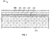
- a cross section of the layers of a photovoltaic cell 20 of a first embodiment not part of the invention has a substrate 210 upon which are deposited the multiple layers used in the photovoltaic cell.
- the first layer deposited on the substrate is a thin film of a transparent conductive layer 220.
- This layer 220 can be a transparent conductive oxide, such as a metallic oxide like tin oxide, which can be doped with, for example, fluorine.
- Layer 230 can be deposited between the front contact and the first semiconductor layer 240, and can have a resistivity sufficiently high to reduce the effects of pinholes in the first semiconductor layer 240. Pinholes in the first semiconductor layer 240 can result in shunt formation between the second semiconductor layer 250 and the first contact resulting in a drain on the local field surrounding the pinhole. A small increase in the resistance of this pathway can dramatically reduce the area affected by the shunt.
- a capping layer 230 can be provided to supply this increase in resistance.
- the capping layer 230 can be a very thin layer of a material with high chemical stability.
- the capping layer 230 can have higher transparency than a comparable thickness of semiconductor material having the same thickness. Examples of materials that are suitable for use as a capping layer include silicon dioxide, dialuminum trioxide, titanium dioxide, diboron trioxide and other similar entities.
- Capping layer 230 can also serve to isolate the transparent conductive layer 220 electrically and chemically from the first semiconductor layer 240 preventing reactions that occur at high temperature that can negatively impact performance and stability.
- the capping layer 230 can also provide a conductive surface that can be more suitable for accepting deposition of the first semiconductor layer 240.
- the capping layer 230 can provide a surface with decreased surface roughness.
- the first semiconductor layer 240 can be thinner than in the absence of the capping layer.
- the first semiconductor layer 240 can have a thickness of greater than about 10 nm and less than about 500 nm.
- the first semiconductor layer can have a thickness greater than 20 nm, greater than 50 nm, greater than 100 nm, or greater than 200 nm and less than 400 nm, less than 300 nm, less than 250 nm, or less than 150 nm.
- the first semiconductor layer 240 can serve as a window layer for the second semiconductor layer 250. By being thinner, the first semiconductor layer 240 allows greater penetration of the shorter wavelengths of the incident light to the second semiconductor layer 250.
- the first semiconductor layer 240 can be a group II-VI, III-V or IV semiconductor, such as, for example, ZnO, ZnS, ZnSe, ZnTe, CdO, CdS, CdSe, CdTe, MgO, MgS, MgSe, MgTe, HgO, HgS, HgSe, HgTe, AlN, AlP, AlAs, AlSb, GaN, GaP, GaAs, GaSb, InN, InP, InAs, InSb, TIN, TIP, TlAs, TlSb, or mixtures thereof.
- the second semiconductor layer 250 can be deposited onto the first semiconductor layer 240.
- the second semiconductor 250 can serve as an absorber layer for the incident light when the first semiconductor layer 240 is serving as a window layer.
- the second semiconductor layer 250 can also be a group II-VI, III-V or IV semiconductor, such as, for example, ZnO, ZnS, ZnSe, ZnTe, CdO, CdS, CdSe, CdTe, MgO, MgS, MgSe, MgTe, HgO, HgS, HgSe, HgTe, AlN, AlP, AlAs, AlSb, GaN, GaP, GaAs, GaSb, InN, InP, InAs, InSb, TIN, TIP, TlAs, TlSb, or mixtures thereof.
- group II-VI, III-V or IV semiconductor such as, for example, ZnO, ZnS, ZnSe, ZnTe, CdO, CdS, CdSe, CdTe, MgO, MgS, MgSe, MgTe, HgO, HgS, HgSe, HgTe, Al
- Metal layer 260 can be a nitrogen-containing metal layer.
- a nitrogen-containing metal layer can include an aluminum nitride, a molybdenum nitride, a nickel nitride, a titanium nitride, a tungsten nitride, a selenium nitride, a tantalum nitride, or a vanadium nitride in contact with the semiconductor layer.
- a nitrogen-containing metal layer can include a stoichiometric nitride.
- a nitrogen-containing metal layer can include a non-stoichiometric nitride, for example, a nitrogen-deficient nitride.
- a nitrogen-containing metal layer can include an aluminum nitride, a nickel nitride, a titanium nitride, a tungsten nitride, a selenium nitride, a tantalum nitride, or a vanadium nitride in contact with the semiconductor layer.
- the metal layer 260 can be deposited on a first semiconductor layer 240 or on a second semiconductor layer 250.
- a photovoltaic cell 30 of a second embodiment further includes a plurality of metal layers, a chromium layer 320 and an aluminum layer 310, the aluminum layer positioned between the chromium layer and a nitrogen containing metal layer 300.
- the photovoltaic cell can also include a chromium layer, a molybdenum nitride, and an aluminum layer in between the chromium layer and the molybdenum nitride (Cr/Al/MoN).
- a nitrogen containing metal layer 300 can be deposited on a second semiconductor layer 550 or on a first semiconductor layer 540.
- the second semiconductor layer can be deposited onto a first semiconductor layer 540.
- a capping layer 530 can serve to isolate a transparent conductive layer 520 electrically and chemically from the first semiconductor layer preventing reactions that occur at high temperature that can negatively impact performance and stability.
- the transparent conductive layer can be deposited on a substrate 510.
- a metal layer can be deposited onto a second semiconductor layer to act as a back metal electrode.
- a metal layer can be a single elemental layer or layers from multiple elements to increase photovoltaic cell efficiency.
- the first metal layer that is directly in contact with the top surface of the second semiconductor can be made more resistive for high photovoltaic cell efficiency.
- the resistivity of the first metal layer can be increased by depositing a metal under nitrogen and argon mixture as an ambient during sputtering. The amount of nitrogen incorporated into the first metal layer, and therefore resistivity, is dependent on the amount of nitrogen available during sputtering. Good photovoltaic cell efficiency results can be obtained when the sputtering ambient is composed of 13% Nitrogen and 87% Argon.
- a first metal layer can include, for example, chromium, molybdenum, nickel, titanium, selenium or tungsten, or alloys thereof.
- a first metal layer can have a thickness of less than 500 nm, less than 100 nm, or less than 10 nm.
- a first metal layer can have a thickness greater than 2 nm and less then 100 nm. Additional layers are subsequently deposited on top of the first metal layer to provide adequate conductivity to transport electrical charges out to external load.
- a second metal layer includes aluminum, using argon as a sputtering gas. The second metal layer can be as thick as 500 nm to as thin as 100 nm, for example.
- the second metal layer is capped with a thin layer of less corrosive chromium to prevent oxidation during subsequent processing or operation of photovoltaic panels.
- the thickness of the capping layer can be as thick as 50 nm to as thin as 10 nm.
- Photovoltaic panels containing molybdenum nitrides have shown an improved efficiency of at least 0.05%, 0.10%, and 0.20% efficiency greater than chromium nitrides.
- devices were finished with appropriate back contacts. Testing for results of these devices was performed at initial efficiency, and after accelerated stress testing using I/V measurements on a solar simulator. For example, photovoltaic panels containing MoN x had a 0.2%-0.4% point higher efficiency than those containing CrN x . Stability of photovoltaic panels under accelerated light soak was carried out for comparison between MoN x and CrN x revealed improved performance of the MoN x devices, with no negative impact on metal layer adhesion.
- the semiconductor layers can include a variety of other materials, as can the materials used for the buffer layer and the capping layer. Accordingly, other embodiments are within the scope of the following claims.
Landscapes
- Photovoltaic Devices (AREA)
- Life Sciences & Earth Sciences (AREA)
- Engineering & Computer Science (AREA)
- Sustainable Energy (AREA)
- Sustainable Development (AREA)
Claims (13)
- Cellule photovoltaïque (30) comprenant :un substrat (510) ;une couche conductrice transparente (520) sur le substrat (510) ;une couche de semi-conducteur (540, 550) comprenant une première couche de semi-conducteur (540),caractérisée par une couche de métal contenant de l'azote (300) en contact avec la couche de semi-conducteur (540, 550), de sorte que la couche de semi-conducteur (540, 550) soit entre la couche de métal contenant de l'azote (300) et la couche d'oxyde conductrice transparente (520),dans laquelle la couche de métal contenant de l'azote (300) comprend l'un parmi un nitrure d'aluminium, un nitrure de molybdène, un nitrure de nickel, un nitrure de titane, un nitrure de tungstène, un nitrure de sélénium, un nitrure de tantale ou un nitrure de vanadium ;une couche de chrome (320) par-dessus la couche de métal contenant de l'azote (300) ; etune couche d'aluminium (310) entre la couche de chrome (320) et la couche de métal contenant de l'azote (300).
- Système de production d'énergie électrique comprenant :la cellule photovoltaïque (30) de la revendication 1 ;une première connexion électrique connectée à la couche conductrice transparente (520) ; etune seconde connexion électrique connectée à la couche de chrome (320).
- Cellule ou système selon l'une quelconque des revendications précédentes, dans lesquels la couche de semi-conducteur comprend une seconde couche de semi-conducteur (550) par-dessus la première couche de semi-conducteur (540).
- Cellule ou système selon l'une quelconque des revendications précédentes, comprenant en outre une couche de recouvrement (530), la couche de recouvrement (530) isolant la couche d'oxyde conductrice transparente (520) d'un contact avec la première couche de semi-conducteur (540).
- Procédé de fabrication d'une cellule photovoltaïque (30) comprenant :le dépôt d'une couche conductrice transparente (520) sur un substrat (510) ;le placement d'une couche de semi-conducteur (540, 550) comprenant une première couche de semi-conducteur (540) sur la couche conductrice transparente (520) ;le dépôt d'une couche de métal sur la couche de semi-conducteur (540, 550) en présence d'azote pour former une couche de métal contenant de l'azote (300), la couche de métal contenant de l'azote (300) comportant un nitrure d'aluminium, un nitrure de molybdène, un nitrure de nickel, un nitrure de titane, un nitrure de tungstène, un nitrure de sélénium, un nitrure de tantale ou un nitrure de vanadium en contact avec la couche de semi-conducteur (540, 550) ;le dépôt d'une couche d'aluminium (310) par-dessus la couche de métal contenant de l'azote (300) ; etle dépôt d'une couche de chrome (320) par-dessus la couche d'aluminium (310).
- Procédé selon la revendication 5, dans lequel la couche de semi-conducteur comprend une seconde couche de semi-conducteur (550) par-dessus la première couche de semi-conducteur (540).
- Procédé selon la revendication 5 ou 6, dans lequel la couche conductrice transparente (520) comprend un oxyde conducteur transparent tel qu'un oxyde d'étain.
- Procédé selon l'une quelconque des revendications 5 à 7, comprenant en outre le placement d'une couche de recouvrement (530) entre la couche conductrice transparente (520) et la première couche de semi-conducteur (540), qui comporte le dépôt d'une couche mince sur la couche conductrice transparente (520).
- Cellule, système ou procédé selon l'une quelconque des revendications 1, 2 et 5, dans lesquels la première couche de semi-conducteur (540) comprend un semi-conducteur binaire tel que le CdS.
- Cellule, système ou procédé selon l'une quelconque des revendications 3 et 6, dans lesquels la première ou seconde couche de semi-conducteur (540, 550) comprend un semi-conducteur binaire tel que le CdTe.
- Cellule, système ou procédé selon l'une quelconque des revendications précédentes, dans lesquels la couche de métal contenant de l'azote (300) comporte un nitrure stoechiométrique.
- Cellule, système ou procédé selon l'une quelconque des revendications 1 à 10, dans lesquels la couche de métal contenant de l'azote (300) comporte un nitrure non stoechiométrique.
- Cellule selon la revendication 1, dans laquelle la couche de métal contenant de l'azote (300) comporte un nitrure de chrome ou un nitrure de molybdène.
Applications Claiming Priority (3)
| Application Number | Priority Date | Filing Date | Title |
|---|---|---|---|
| US86470906P | 2006-11-07 | 2006-11-07 | |
| US11/935,112 US9147778B2 (en) | 2006-11-07 | 2007-11-05 | Photovoltaic devices including nitrogen-containing metal contact |
| PCT/US2007/083758 WO2008058119A2 (fr) | 2006-11-07 | 2007-11-06 | Dispositifs photovoltaïques comprenant un contact métallique contenant de l'azote |
Publications (3)
| Publication Number | Publication Date |
|---|---|
| EP2080229A2 EP2080229A2 (fr) | 2009-07-22 |
| EP2080229A4 EP2080229A4 (fr) | 2016-04-13 |
| EP2080229B1 true EP2080229B1 (fr) | 2017-10-11 |
Family
ID=39365307
Family Applications (1)
| Application Number | Title | Priority Date | Filing Date |
|---|---|---|---|
| EP07844909.7A Active EP2080229B1 (fr) | 2006-11-07 | 2007-11-06 | Dispositifs photovoltaïques comprenant un contact métallique contenant de l'azote |
Country Status (5)
| Country | Link |
|---|---|
| US (4) | US9147778B2 (fr) |
| EP (1) | EP2080229B1 (fr) |
| MX (1) | MX2009004895A (fr) |
| MY (1) | MY171673A (fr) |
| WO (1) | WO2008058119A2 (fr) |
Families Citing this family (30)
| Publication number | Priority date | Publication date | Assignee | Title |
|---|---|---|---|---|
| US9147778B2 (en) | 2006-11-07 | 2015-09-29 | First Solar, Inc. | Photovoltaic devices including nitrogen-containing metal contact |
| KR101614554B1 (ko) | 2007-11-02 | 2016-04-21 | 퍼스트 솔라, 인코포레이티드 | 도핑된 반도체 막을 포함하는 광기전 장치 |
| WO2010068282A2 (fr) * | 2008-12-10 | 2010-06-17 | The Regents Of The University Of California | Compositions et procédés pour la synthèse de combustible à base d'hydrogène |
| WO2010126699A2 (fr) | 2009-04-29 | 2010-11-04 | Hunter Douglas Industries B.V. | Panneaux architecturaux à intercouches photovoltaïques organiques et leurs procédés de formation |
| US8262894B2 (en) | 2009-04-30 | 2012-09-11 | Moses Lake Industries, Inc. | High speed copper plating bath |
| WO2010141463A1 (fr) * | 2009-06-04 | 2010-12-09 | First Solar, Inc. | Matériau de contact contenant un dopant |
| US20100307568A1 (en) * | 2009-06-04 | 2010-12-09 | First Solar, Inc. | Metal barrier-doped metal contact layer |
| US8841541B2 (en) * | 2009-09-04 | 2014-09-23 | Mitsubishi Electric Corporation | Solar battery and method of manufacturing the same |
| WO2011057189A1 (fr) * | 2009-11-08 | 2011-05-12 | First Solar, Inc. | Dépôt de matériau de contact repos au moyen de mélanges de gaz dopés à l'eau |
| IN2012DN05898A (fr) * | 2009-12-18 | 2015-09-18 | First Solar Inc | |
| WO2011123117A1 (fr) * | 2010-03-31 | 2011-10-06 | University Of Rochester | Cellules photovoltaïques à contact électrique amélioré |
| US9461186B2 (en) | 2010-07-15 | 2016-10-04 | First Solar, Inc. | Back contact for a photovoltaic module |
| KR101846337B1 (ko) | 2011-11-09 | 2018-04-09 | 엘지이노텍 주식회사 | 태양전지 및 이의 제조방법 |
| CN104081544B (zh) * | 2012-01-13 | 2019-01-22 | 应用材料公司 | 用于硅基光电装置的高功函数缓冲层 |
| US9698285B2 (en) | 2013-02-01 | 2017-07-04 | First Solar, Inc. | Photovoltaic device including a P-N junction and method of manufacturing |
| JP6611701B2 (ja) * | 2013-03-15 | 2019-11-27 | アーケマ・インコーポレイテッド | 窒素含有透明導電性酸化物キャップ層組成物 |
| US11876140B2 (en) | 2013-05-02 | 2024-01-16 | First Solar, Inc. | Photovoltaic devices and method of making |
| CN104183663B (zh) | 2013-05-21 | 2017-04-12 | 第一太阳能马来西亚有限公司 | 光伏器件及其制备方法 |
| CN103290367B (zh) * | 2013-05-29 | 2015-02-11 | 哈尔滨工业大学 | 一种薄膜体声波谐振器下电极的制备方法 |
| US10062800B2 (en) | 2013-06-07 | 2018-08-28 | First Solar, Inc. | Photovoltaic devices and method of making |
| WO2015126918A1 (fr) * | 2014-02-19 | 2015-08-27 | Lucintech, Inc. | Cellules photovoltaïques souples et procédé de production de celles-ci |
| US10529883B2 (en) * | 2014-11-03 | 2020-01-07 | First Solar, Inc. | Photovoltaic devices and method of manufacturing |
| AU2017343630B2 (en) | 2016-10-12 | 2021-08-05 | First Solar, Inc. | Photovoltaic device with transparent tunnel junction |
| CN111670504B (zh) | 2017-12-07 | 2024-01-30 | 第一阳光公司 | 具有v族掺杂剂的光伏器件和半导体层以及用于形成该光伏器件和该半导体层的方法 |
| MY206714A (en) | 2018-10-24 | 2025-01-03 | First Solar Inc | Buffer layers for photovoltaic devices with group v doping |
| EP3903352B1 (fr) | 2018-12-27 | 2022-03-30 | First Solar, Inc. | Dispositifs photovoltaïques et leurs procédés de fabrication |
| CN109830561B (zh) * | 2019-02-20 | 2021-09-03 | 成都中建材光电材料有限公司 | 一种碲化镉薄膜太阳能电池组件及其制备方法 |
| US11257978B2 (en) * | 2019-03-29 | 2022-02-22 | Utica Leaseco, Llc | Front metal contact stack |
| WO2022174055A1 (fr) | 2021-02-12 | 2022-08-18 | First Solar, Inc. | Contacts arrière multicouches pour dispositifs photovoltaïques en pérovskite |
| CN118281090B (zh) * | 2024-05-24 | 2024-10-11 | 通威太阳能(安徽)有限公司 | 太阳电池及其制备方法、生产设备 |
Family Cites Families (34)
| Publication number | Priority date | Publication date | Assignee | Title |
|---|---|---|---|---|
| BR7507192A (pt) * | 1974-11-08 | 1976-08-10 | Western Electric Co | Celula fotovoltaica e processo para sua fabricacao |
| US4064522A (en) * | 1976-02-04 | 1977-12-20 | Exxon Research & Engineering Co. | High efficiency selenium heterojunction solar cells |
| US4197141A (en) * | 1978-01-31 | 1980-04-08 | Massachusetts Institute Of Technology | Method for passivating imperfections in semiconductor materials |
| US4259122A (en) * | 1978-12-08 | 1981-03-31 | Exxon Research And Engineering Co. | Selenium photovoltaic device |
| US4320248A (en) * | 1979-08-13 | 1982-03-16 | Shunpei Yamazaki | Semiconductor photoelectric conversion device |
| US4260428A (en) * | 1980-03-05 | 1981-04-07 | Ses, Incorporated | Photovoltaic cell |
| US4338482A (en) * | 1981-02-17 | 1982-07-06 | Roy G. Gordon | Photovoltaic cell |
| US4582764A (en) * | 1982-09-24 | 1986-04-15 | Energy Conversion Devices, Inc. | Selective absorber amorphous alloys and devices |
| US4485265A (en) * | 1982-11-22 | 1984-11-27 | President And Fellows Of Harvard College | Photovoltaic cell |
| JPS59147469A (ja) * | 1983-02-14 | 1984-08-23 | Hitachi Ltd | 非晶質シリコン太陽電池 |
| US4598306A (en) * | 1983-07-28 | 1986-07-01 | Energy Conversion Devices, Inc. | Barrier layer for photovoltaic devices |
| US4568792A (en) | 1984-02-02 | 1986-02-04 | Sri International | Photovoltaic cell including doped cadmium telluride, a dislocation preventing agent and improved ohmic contacts |
| AU616736B2 (en) * | 1988-03-03 | 1991-11-07 | Asahi Glass Company Limited | Amorphous oxide film and article having such film thereon |
| US5136346A (en) * | 1990-09-07 | 1992-08-04 | Motorola, Inc. | Photon stimulated variable capacitance effect devices |
| US5248349A (en) * | 1992-05-12 | 1993-09-28 | Solar Cells, Inc. | Process for making photovoltaic devices and resultant product |
| US6541695B1 (en) * | 1992-09-21 | 2003-04-01 | Thomas Mowles | High efficiency solar photovoltaic cells produced with inexpensive materials by processes suitable for large volume production |
| US5385848A (en) * | 1993-09-20 | 1995-01-31 | Iowa Thin Film Technologies, Inc | Method for fabricating an interconnected array of semiconductor devices |
| DE4333407C1 (de) * | 1993-09-30 | 1994-11-17 | Siemens Ag | Solarzelle mit einer Chalkopyritabsorberschicht |
| JPH1154773A (ja) * | 1997-08-01 | 1999-02-26 | Canon Inc | 光起電力素子及びその製造方法 |
| US6852614B1 (en) * | 2000-03-24 | 2005-02-08 | University Of Maine | Method of manufacturing semiconductor having group II-group VI compounds doped with nitrogen |
| FR2820241B1 (fr) * | 2001-01-31 | 2003-09-19 | Saint Gobain | Substrat transparent muni d'une electrode |
| JP4560245B2 (ja) * | 2001-06-29 | 2010-10-13 | キヤノン株式会社 | 光起電力素子 |
| US20060006482A1 (en) * | 2002-07-16 | 2006-01-12 | Stmicroelectronics N.V. | Tfa image sensor with stability-optimized photodiode |
| WO2004032189A2 (fr) * | 2002-09-30 | 2004-04-15 | Miasolé | Appareil et procede de fabrication conçus pour produire a grande echelle de cellules solaires a film mince |
| US7141863B1 (en) * | 2002-11-27 | 2006-11-28 | University Of Toledo | Method of making diode structures |
| US7123638B2 (en) * | 2003-10-17 | 2006-10-17 | Avago Technologies General Ip (Singapore) Pte. Ltd. | Tunnel-junction structure incorporating N-type layer comprising nitrogen and a group VI dopant |
| US7663057B2 (en) * | 2004-02-19 | 2010-02-16 | Nanosolar, Inc. | Solution-based fabrication of photovoltaic cell |
| SE0400631D0 (sv) * | 2004-03-11 | 2004-03-11 | Forskarpatent I Uppsala Ab | Thin film solar cell and manufacturing method |
| CN100573812C (zh) * | 2004-03-15 | 2009-12-23 | 索罗能源公司 | 用于太阳能电池制造的沉积半导体薄层的技术和装置 |
| US7405143B2 (en) * | 2004-03-25 | 2008-07-29 | Asm International N.V. | Method for fabricating a seed layer |
| US20050257824A1 (en) * | 2004-05-24 | 2005-11-24 | Maltby Michael G | Photovoltaic cell including capping layer |
| US7288332B2 (en) * | 2005-10-06 | 2007-10-30 | Los Almos National Security, Llc | Conductive layer for biaxially oriented semiconductor film growth |
| US8373060B2 (en) | 2006-10-24 | 2013-02-12 | Zetta Research and Development LLC—AQT Series | Semiconductor grain microstructures for photovoltaic cells |
| US9147778B2 (en) | 2006-11-07 | 2015-09-29 | First Solar, Inc. | Photovoltaic devices including nitrogen-containing metal contact |
-
2007
- 2007-11-05 US US11/935,112 patent/US9147778B2/en active Active
- 2007-11-06 WO PCT/US2007/083758 patent/WO2008058119A2/fr not_active Ceased
- 2007-11-06 EP EP07844909.7A patent/EP2080229B1/fr active Active
- 2007-11-06 MX MX2009004895A patent/MX2009004895A/es active IP Right Grant
- 2007-11-06 MY MYPI20091849A patent/MY171673A/en unknown
-
2015
- 2015-09-08 US US14/847,738 patent/US20150380601A1/en not_active Abandoned
-
2019
- 2019-01-11 US US16/245,613 patent/US11695085B2/en active Active
-
2023
- 2023-06-06 US US18/206,430 patent/US20230317864A1/en not_active Abandoned
Non-Patent Citations (1)
| Title |
|---|
| None * |
Also Published As
| Publication number | Publication date |
|---|---|
| US11695085B2 (en) | 2023-07-04 |
| US20230317864A1 (en) | 2023-10-05 |
| US9147778B2 (en) | 2015-09-29 |
| WO2008058119A2 (fr) | 2008-05-15 |
| MY171673A (en) | 2019-10-23 |
| US20190148571A1 (en) | 2019-05-16 |
| US20150380601A1 (en) | 2015-12-31 |
| MX2009004895A (es) | 2009-05-19 |
| US20080110498A1 (en) | 2008-05-15 |
| EP2080229A4 (fr) | 2016-04-13 |
| WO2008058119A3 (fr) | 2008-08-21 |
| EP2080229A2 (fr) | 2009-07-22 |
Similar Documents
| Publication | Publication Date | Title |
|---|---|---|
| US20230317864A1 (en) | Photovoltaic Devices Including Nitrogen-Containing Metal Contact | |
| US11843070B2 (en) | Photovoltaic devices including doped semiconductor films | |
| AU2005330568B2 (en) | Photovoltaic cell including capping layer | |
| US8198529B2 (en) | Transparent conductive materials including cadmium stannate | |
| US20080128020A1 (en) | Photovoltaic devices including a metal stack | |
| US20110136294A1 (en) | Plasma-Treated Photovoltaic Devices | |
| US20100206372A1 (en) | Photovoltaic Devices Including Heterojunctions | |
| US20170077345A1 (en) | Photovoltaic devices including controlled copper uptake | |
| US20100212730A1 (en) | Photovoltaic devices including back metal contacts | |
| US20080128022A1 (en) | Photovoltaic device including a tin oxide protective layer |
Legal Events
| Date | Code | Title | Description |
|---|---|---|---|
| PUAI | Public reference made under article 153(3) epc to a published international application that has entered the european phase |
Free format text: ORIGINAL CODE: 0009012 |
|
| 17P | Request for examination filed |
Effective date: 20090528 |
|
| AK | Designated contracting states |
Kind code of ref document: A2 Designated state(s): AT BE BG CH CY CZ DE DK EE ES FI FR GB GR HU IE IS IT LI LT LU LV MC MT NL PL PT RO SE SI SK TR |
|
| RIN1 | Information on inventor provided before grant (corrected) |
Inventor name: STEELE, MICHAEL T. Inventor name: JAYAMAHA, UPALI Inventor name: ZAFAR, SYED |
|
| DAX | Request for extension of the european patent (deleted) | ||
| A4 | Supplementary search report drawn up and despatched |
Effective date: 20160315 |
|
| RIC1 | Information provided on ipc code assigned before grant |
Ipc: H01L 31/00 20060101AFI20160309BHEP |
|
| GRAP | Despatch of communication of intention to grant a patent |
Free format text: ORIGINAL CODE: EPIDOSNIGR1 |
|
| STAA | Information on the status of an ep patent application or granted ep patent |
Free format text: STATUS: GRANT OF PATENT IS INTENDED |
|
| INTG | Intention to grant announced |
Effective date: 20170509 |
|
| INTG | Intention to grant announced |
Effective date: 20170515 |
|
| GRAS | Grant fee paid |
Free format text: ORIGINAL CODE: EPIDOSNIGR3 |
|
| GRAA | (expected) grant |
Free format text: ORIGINAL CODE: 0009210 |
|
| STAA | Information on the status of an ep patent application or granted ep patent |
Free format text: STATUS: THE PATENT HAS BEEN GRANTED |
|
| GRAT | Correction requested after decision to grant or after decision to maintain patent in amended form |
Free format text: ORIGINAL CODE: EPIDOSNCDEC |
|
| AK | Designated contracting states |
Kind code of ref document: B1 Designated state(s): AT BE BG CH CY CZ DE DK EE ES FI FR GB GR HU IE IS IT LI LT LU LV MC MT NL PL PT RO SE SI SK TR |
|
| REG | Reference to a national code |
Ref country code: GB Ref legal event code: FG4D |
|
| REG | Reference to a national code |
Ref country code: CH Ref legal event code: EP |
|
| REG | Reference to a national code |
Ref country code: IE Ref legal event code: FG4D |
|
| REG | Reference to a national code |
Ref country code: AT Ref legal event code: REF Ref document number: 936747 Country of ref document: AT Kind code of ref document: T Effective date: 20171115 |
|
| REG | Reference to a national code |
Ref country code: DE Ref legal event code: R096 Ref document number: 602007052683 Country of ref document: DE |
|
| REG | Reference to a national code |
Ref country code: FR Ref legal event code: PLFP Year of fee payment: 11 |
|
| REG | Reference to a national code |
Ref country code: NL Ref legal event code: MP Effective date: 20171011 |
|
| REG | Reference to a national code |
Ref country code: LT Ref legal event code: MG4D |
|
| REG | Reference to a national code |
Ref country code: AT Ref legal event code: MK05 Ref document number: 936747 Country of ref document: AT Kind code of ref document: T Effective date: 20171011 |
|
| PG25 | Lapsed in a contracting state [announced via postgrant information from national office to epo] |
Ref country code: NL Free format text: LAPSE BECAUSE OF FAILURE TO SUBMIT A TRANSLATION OF THE DESCRIPTION OR TO PAY THE FEE WITHIN THE PRESCRIBED TIME-LIMIT Effective date: 20171011 |
|
| PG25 | Lapsed in a contracting state [announced via postgrant information from national office to epo] |
Ref country code: FI Free format text: LAPSE BECAUSE OF FAILURE TO SUBMIT A TRANSLATION OF THE DESCRIPTION OR TO PAY THE FEE WITHIN THE PRESCRIBED TIME-LIMIT Effective date: 20171011 Ref country code: SE Free format text: LAPSE BECAUSE OF FAILURE TO SUBMIT A TRANSLATION OF THE DESCRIPTION OR TO PAY THE FEE WITHIN THE PRESCRIBED TIME-LIMIT Effective date: 20171011 Ref country code: LT Free format text: LAPSE BECAUSE OF FAILURE TO SUBMIT A TRANSLATION OF THE DESCRIPTION OR TO PAY THE FEE WITHIN THE PRESCRIBED TIME-LIMIT Effective date: 20171011 Ref country code: ES Free format text: LAPSE BECAUSE OF FAILURE TO SUBMIT A TRANSLATION OF THE DESCRIPTION OR TO PAY THE FEE WITHIN THE PRESCRIBED TIME-LIMIT Effective date: 20171011 |
|
| PG25 | Lapsed in a contracting state [announced via postgrant information from national office to epo] |
Ref country code: GR Free format text: LAPSE BECAUSE OF FAILURE TO SUBMIT A TRANSLATION OF THE DESCRIPTION OR TO PAY THE FEE WITHIN THE PRESCRIBED TIME-LIMIT Effective date: 20180112 Ref country code: AT Free format text: LAPSE BECAUSE OF FAILURE TO SUBMIT A TRANSLATION OF THE DESCRIPTION OR TO PAY THE FEE WITHIN THE PRESCRIBED TIME-LIMIT Effective date: 20171011 Ref country code: BG Free format text: LAPSE BECAUSE OF FAILURE TO SUBMIT A TRANSLATION OF THE DESCRIPTION OR TO PAY THE FEE WITHIN THE PRESCRIBED TIME-LIMIT Effective date: 20180111 Ref country code: IS Free format text: LAPSE BECAUSE OF FAILURE TO SUBMIT A TRANSLATION OF THE DESCRIPTION OR TO PAY THE FEE WITHIN THE PRESCRIBED TIME-LIMIT Effective date: 20180211 Ref country code: LV Free format text: LAPSE BECAUSE OF FAILURE TO SUBMIT A TRANSLATION OF THE DESCRIPTION OR TO PAY THE FEE WITHIN THE PRESCRIBED TIME-LIMIT Effective date: 20171011 |
|
| REG | Reference to a national code |
Ref country code: DE Ref legal event code: R097 Ref document number: 602007052683 Country of ref document: DE |
|
| PG25 | Lapsed in a contracting state [announced via postgrant information from national office to epo] |
Ref country code: LI Free format text: LAPSE BECAUSE OF NON-PAYMENT OF DUE FEES Effective date: 20171130 Ref country code: MC Free format text: LAPSE BECAUSE OF FAILURE TO SUBMIT A TRANSLATION OF THE DESCRIPTION OR TO PAY THE FEE WITHIN THE PRESCRIBED TIME-LIMIT Effective date: 20171011 Ref country code: CZ Free format text: LAPSE BECAUSE OF FAILURE TO SUBMIT A TRANSLATION OF THE DESCRIPTION OR TO PAY THE FEE WITHIN THE PRESCRIBED TIME-LIMIT Effective date: 20171011 Ref country code: CH Free format text: LAPSE BECAUSE OF NON-PAYMENT OF DUE FEES Effective date: 20171130 Ref country code: SK Free format text: LAPSE BECAUSE OF FAILURE TO SUBMIT A TRANSLATION OF THE DESCRIPTION OR TO PAY THE FEE WITHIN THE PRESCRIBED TIME-LIMIT Effective date: 20171011 Ref country code: EE Free format text: LAPSE BECAUSE OF FAILURE TO SUBMIT A TRANSLATION OF THE DESCRIPTION OR TO PAY THE FEE WITHIN THE PRESCRIBED TIME-LIMIT Effective date: 20171011 Ref country code: DK Free format text: LAPSE BECAUSE OF FAILURE TO SUBMIT A TRANSLATION OF THE DESCRIPTION OR TO PAY THE FEE WITHIN THE PRESCRIBED TIME-LIMIT Effective date: 20171011 |
|
| PLBE | No opposition filed within time limit |
Free format text: ORIGINAL CODE: 0009261 |
|
| STAA | Information on the status of an ep patent application or granted ep patent |
Free format text: STATUS: NO OPPOSITION FILED WITHIN TIME LIMIT |
|
| PG25 | Lapsed in a contracting state [announced via postgrant information from national office to epo] |
Ref country code: PL Free format text: LAPSE BECAUSE OF FAILURE TO SUBMIT A TRANSLATION OF THE DESCRIPTION OR TO PAY THE FEE WITHIN THE PRESCRIBED TIME-LIMIT Effective date: 20171011 Ref country code: IT Free format text: LAPSE BECAUSE OF FAILURE TO SUBMIT A TRANSLATION OF THE DESCRIPTION OR TO PAY THE FEE WITHIN THE PRESCRIBED TIME-LIMIT Effective date: 20171011 Ref country code: RO Free format text: LAPSE BECAUSE OF FAILURE TO SUBMIT A TRANSLATION OF THE DESCRIPTION OR TO PAY THE FEE WITHIN THE PRESCRIBED TIME-LIMIT Effective date: 20171011 Ref country code: LU Free format text: LAPSE BECAUSE OF NON-PAYMENT OF DUE FEES Effective date: 20171106 |
|
| REG | Reference to a national code |
Ref country code: BE Ref legal event code: MM Effective date: 20171130 |
|
| REG | Reference to a national code |
Ref country code: IE Ref legal event code: MM4A |
|
| 26N | No opposition filed |
Effective date: 20180712 |
|
| GBPC | Gb: european patent ceased through non-payment of renewal fee |
Effective date: 20180111 |
|
| PG25 | Lapsed in a contracting state [announced via postgrant information from national office to epo] |
Ref country code: MT Free format text: LAPSE BECAUSE OF NON-PAYMENT OF DUE FEES Effective date: 20171106 |
|
| PG25 | Lapsed in a contracting state [announced via postgrant information from national office to epo] |
Ref country code: IE Free format text: LAPSE BECAUSE OF NON-PAYMENT OF DUE FEES Effective date: 20171106 |
|
| PG25 | Lapsed in a contracting state [announced via postgrant information from national office to epo] |
Ref country code: GB Free format text: LAPSE BECAUSE OF NON-PAYMENT OF DUE FEES Effective date: 20180111 Ref country code: BE Free format text: LAPSE BECAUSE OF NON-PAYMENT OF DUE FEES Effective date: 20171130 Ref country code: SI Free format text: LAPSE BECAUSE OF FAILURE TO SUBMIT A TRANSLATION OF THE DESCRIPTION OR TO PAY THE FEE WITHIN THE PRESCRIBED TIME-LIMIT Effective date: 20171011 |
|
| PG25 | Lapsed in a contracting state [announced via postgrant information from national office to epo] |
Ref country code: HU Free format text: LAPSE BECAUSE OF FAILURE TO SUBMIT A TRANSLATION OF THE DESCRIPTION OR TO PAY THE FEE WITHIN THE PRESCRIBED TIME-LIMIT; INVALID AB INITIO Effective date: 20071106 |
|
| PG25 | Lapsed in a contracting state [announced via postgrant information from national office to epo] |
Ref country code: CY Free format text: LAPSE BECAUSE OF NON-PAYMENT OF DUE FEES Effective date: 20171011 |
|
| PG25 | Lapsed in a contracting state [announced via postgrant information from national office to epo] |
Ref country code: TR Free format text: LAPSE BECAUSE OF FAILURE TO SUBMIT A TRANSLATION OF THE DESCRIPTION OR TO PAY THE FEE WITHIN THE PRESCRIBED TIME-LIMIT Effective date: 20171011 |
|
| PG25 | Lapsed in a contracting state [announced via postgrant information from national office to epo] |
Ref country code: PT Free format text: LAPSE BECAUSE OF FAILURE TO SUBMIT A TRANSLATION OF THE DESCRIPTION OR TO PAY THE FEE WITHIN THE PRESCRIBED TIME-LIMIT Effective date: 20171011 |
|
| REG | Reference to a national code |
Ref country code: DE Ref legal event code: R082 Ref document number: 602007052683 Country of ref document: DE Representative=s name: D YOUNG & CO LLP, DE |
|
| P01 | Opt-out of the competence of the unified patent court (upc) registered |
Effective date: 20230518 |
|
| REG | Reference to a national code |
Ref country code: DE Ref legal event code: R079 Ref document number: 602007052683 Country of ref document: DE Free format text: PREVIOUS MAIN CLASS: H01L0031000000 Ipc: H10F0077000000 |
|
| PGFP | Annual fee paid to national office [announced via postgrant information from national office to epo] |
Ref country code: DE Payment date: 20251128 Year of fee payment: 19 |
|
| PGFP | Annual fee paid to national office [announced via postgrant information from national office to epo] |
Ref country code: FR Payment date: 20251125 Year of fee payment: 19 |