EP2087366B1 - Procédé et appareil de détection de la polarisation en spin des porteurs - Google Patents
Procédé et appareil de détection de la polarisation en spin des porteurs Download PDFInfo
- Publication number
- EP2087366B1 EP2087366B1 EP07824084A EP07824084A EP2087366B1 EP 2087366 B1 EP2087366 B1 EP 2087366B1 EP 07824084 A EP07824084 A EP 07824084A EP 07824084 A EP07824084 A EP 07824084A EP 2087366 B1 EP2087366 B1 EP 2087366B1
- Authority
- EP
- European Patent Office
- Prior art keywords
- spin
- subject material
- subject
- carriers
- semiconductor
- Prior art date
- Legal status (The legal status is an assumption and is not a legal conclusion. Google has not performed a legal analysis and makes no representation as to the accuracy of the status listed.)
- Not-in-force
Links
Images


Classifications
-
- G—PHYSICS
- G01—MEASURING; TESTING
- G01R—MEASURING ELECTRIC VARIABLES; MEASURING MAGNETIC VARIABLES
- G01R33/00—Arrangements or instruments for measuring magnetic variables
- G01R33/02—Measuring direction or magnitude of magnetic fields or magnetic flux
- G01R33/06—Measuring direction or magnitude of magnetic fields or magnetic flux using galvano-magnetic devices
- G01R33/09—Magnetoresistive devices
- G01R33/093—Magnetoresistive devices using multilayer structures, e.g. giant magnetoresistance sensors
-
- B—PERFORMING OPERATIONS; TRANSPORTING
- B82—NANOTECHNOLOGY
- B82Y—SPECIFIC USES OR APPLICATIONS OF NANOSTRUCTURES; MEASUREMENT OR ANALYSIS OF NANOSTRUCTURES; MANUFACTURE OR TREATMENT OF NANOSTRUCTURES
- B82Y25/00—Nanomagnetism, e.g. magnetoimpedance, anisotropic magnetoresistance, giant magnetoresistance or tunneling magnetoresistance
-
- G—PHYSICS
- G01—MEASURING; TESTING
- G01R—MEASURING ELECTRIC VARIABLES; MEASURING MAGNETIC VARIABLES
- G01R33/00—Arrangements or instruments for measuring magnetic variables
- G01R33/12—Measuring magnetic properties of articles or specimens of solids or fluids
-
- G—PHYSICS
- G01—MEASURING; TESTING
- G01R—MEASURING ELECTRIC VARIABLES; MEASURING MAGNETIC VARIABLES
- G01R33/00—Arrangements or instruments for measuring magnetic variables
- G01R33/12—Measuring magnetic properties of articles or specimens of solids or fluids
- G01R33/1238—Measuring superconductive properties
-
- H—ELECTRICITY
- H10—SEMICONDUCTOR DEVICES; ELECTRIC SOLID-STATE DEVICES NOT OTHERWISE PROVIDED FOR
- H10N—ELECTRIC SOLID-STATE DEVICES NOT OTHERWISE PROVIDED FOR
- H10N50/00—Galvanomagnetic devices
- H10N50/10—Magnetoresistive devices
-
- H—ELECTRICITY
- H10—SEMICONDUCTOR DEVICES; ELECTRIC SOLID-STATE DEVICES NOT OTHERWISE PROVIDED FOR
- H10N—ELECTRIC SOLID-STATE DEVICES NOT OTHERWISE PROVIDED FOR
- H10N52/00—Hall-effect devices
- H10N52/101—Semiconductor Hall-effect devices
Definitions
- the present invention relates to a method for the detection, measurement and transport of spin polarized carriers and to an apparatus for performing the same.
- US 6,369,404 discloses a device for the measurement of single electron and nuclear spins.
- the device comprises a semiconductor substrate, onto which is introduced at least one donor atom to produce a donor nuclear spin electron system having large electron wave functions at the nucleus of the donor atom.
- An insulating layer extends across the substrate, to which is attached first and second conducting gates.
- the first gate controls the energy of the bound electron state at the donor atom.
- the second gate is used to generate at least one additional electron in the substrate.
- the gates are biased to move the additional electron to the donor atom in the substrate, when the spins of the additional electron and donor electron or nucleus so permit.
- US 6,403,999 discloses a method and apparatus for the detection of free electrons with a selected spin polarization within a semiconductor material.
- the method involves applying a static magnetic field and an electromagnetic field to the semiconductor, during which free electrons are injected into the semiconductor by way of diffusion or tunneling techniques from a ferromagnetic material.
- the movement of the spin polarized electrons within the semiconductor gives rise to a Hall voltage across the semiconductor by virtue of the applied magnetic field and the Hall effect.
- the measurement of this Hall voltage is used to estimate a concentration of free electrons with a given spin.
- This method relies upon the application of magnetic fields and the resulting Hall effect voltage arising from the movement of the electrons within the semiconductor.
- EP 1 659 416 concerns a method and apparatus for spin detection.
- the method for detecting spin polarization in a medium comprises measuring a first current on a first contact with the medium having a first spin selectivity, measuring a second current on a second contact with the medium having a second spin selectivity, and deriving an average or statistically relevant spin state from a comparison of the first and second currents.
- the selectivity of the first and second contacts to the spin is achieved using a combination of materials having different magnetic properties.
- spin tunneling is a technique by which spin polarized carriers, in particular electrons, are caused to pass from a source material into a second material.
- the technique has been known for some time and observed in the case of two ferromagnetic materials.
- Pan, F.M., et al. 'Transport Properties on La0.7Sr0.3MnO3/Al2O3/Fe Tunnel Junctions', Journal of Zhejiang University Science, 2000, Vol. 1, No. 2, pages 121 to 124 describes experiments in which the transport of spin polarized electrons between a layer of LaSrMnO and a layer of iron was observed.
- the aforementioned layers were separated by an insulating layer of alumina (Al 2 O 3 ).
- Van Dorpe, P. et al., 'Highly Efficient Room Temperature Spin Injection in a Metal-Insulator-Semiconductor Light-Emitting Diode', Jpn. J. Appl. Phys. Vol. 42, No.5B, pages L502 to L504 describe similar experiments to demonstrate the efficiency of spin injection into an AlGaAs/GaAs semiconductor from a CoFe/AlO x tunnel spin injector.
- WO 2005/109517 discloses a semiconductor device using location and the sign of the spin of electrons and having a spin valve structure.
- the device comprises a ferromagnetic layer on a substrate having a tunnel barrier layer.
- a multilayered structure is disclosed, an example being a Ga 0.94 Mn 0.06 As/GaAs/Ga 0.94 Mn 0.06 As trilayer structure.
- AR Andreev Reflection
- a current in a metal or semiconductor is converted to a supercurrent at the junction with a superconductor.
- an electron approaching a junction with a superconductor must be a member of an electron pair (known as a 'Cooper pair'), in order to proceed and form part of the supercurrent.
- the second electron required to form the electron pair in the superconductor is provided by the metal, forming a hole at the interface.
- the hole is reflected and propogates away from the interface through the metal, as the electron pair enters the superconductor.
- the action of the reflected hole is that of a parallel conduction channel, which has the effect of increasing the conductance of the normal state metal by 100%.
- Superconducting electron pairs consist of a spin-up electron and a spin-down electron.
- a spin-up electron at the interface requires a spin-down electron to be removed from the metal to form the spin neutral supercurrent. This leaves a spin-up hole to propagate away from the interface through the metal.
- a spin-down electron at the interface will propagate a spin-up hole.
- the effect is to reduce the conductance.
- AR has been recognized as being of use in the measurement of spin polarization within a metal.
- US 6,403,999 is concerned with the detection of polarized spin transport in semiconductors, in particular the estimation of the concentration of free electrons with selected spin polarisations in a semiconductor material.
- US 2006/002220 discloses a spin-injection device and magnetic device using the same.
- the present invention provides a method of detecting spin polarization in a subject material, the method comprising:
- Tunnelling magnetoresistance is a measure of the tunneling resistance of carriers flowing between a first ferromagnetic layer and a second layer of ferromagnetic material or a semiconductor.
- spin polarized electrons are caused to pass from the subject material into the ferromagnetic material when the magnetic orientation of the ferromagnetic material is parallel with the spin orientation in the subject material.
- TMR is dependent upon the relative spin orientation in the two materials.
- measurement of the TMR when the Spin Hall Effect (SHE) is generated in the subject material will allow a determination of the extent of spin polarization in the subject material. Techniques for measuring TMR suitable for use in the method of the present invention are known in the art.
- the spin Hall effect is a phenomenon analogous to the Hall effect known and employed in conventional electronic systems.
- the Hall effect is the production of a potential difference across a material when a current is caused to flow through the material in the presence of an applied magnetic field.
- the potential difference, the Hall voltage is established perpendicular to the applied electrical and magnetic fields.
- the SHE manifests itself as the concentration of electrons of a given spin at one side of a material when an electrical current is caused to flow through the material.
- the polarization of carriers according to their spin occurs perpendicular to the applied electric field.
- the SHE arises without the application of a magnetic field to the material. It should be noted that the SHE, while polarizing the carriers according to their spin, does not give rise to an electrical potential difference across the material, the spin polarized carriers being distributed in a neutral charge pattern.
- the SHE has also been detected optically at room temperature in n-type ZnSe epilayers using Kerr rotation spectroscopy by Stern, N.P. et al., 'Current-Induced Polarization and the Spin Hall Effect at Room Temperature', arXiv:cond-mat/0607288 v1, July 11, 2006 .
- an electric field is applied to the subject material, such that a current passes through the subject material, in order to induce the SHE, thus spin polarizing the carriers, such that carriers having a first spin orientation flow along a first edge of the subject material and carriers having the opposite spin orientation flow along the opposite, second edge of the subject material, the direction of spin polarization being perpendicular to the applied electric field.
- an electric field is applied across the subject material, in order to generate the SHE.
- the electric field to the subject material is of sufficient strength to induce the SHE.
- the electric field applied is typically in the range of from up to 250 mV/ ⁇ m, more preferably from 0 to 100 mV/ ⁇ m.
- the transport of spin polarized carriers may be carried out using spin tunneling techniques known in the art, such as those described in the prior art documents discussed hereinbefore.
- the spin polarized carriers may be holes or electrons, most preferably electrons.
- spin injection is achieved using a ferromagnetic material as a source of spin polarized carriers.
- the tunneling of spin polarized carriers is achieved by applying a first magnetic field to the ferromagnetic material, inducing a first spin polarization in carriers in the ferromagnetic material, and a second magnetic field, to a second material to induce a second spin polarization in the carriers in the second material.
- the injection of spin polarized carriers may occur from the ferromagnetic source material into the second material, as the spin orientations in the two materials are the same.
- the spin injection efficiency reduces as the first and second magnetic fields are moved out of alignment, and hence the spin orientation changes, until the efficiency drops to zero when the first and second magnetic fields are antiparallel.
- spin polarization of the carriers is induced as a result of the SHE and not by the application of a magnetic field.
- the application of a magnetic field to a ferromagnetic material orients the spin polarization of the carriers in the ferromagnetic material, according to the orientation of the applied magnetic field. This spin orientation remains once the ferromagnetic material is removed from the magnetic field and until the material is subjected to a further magnetic field to change the orientation.
- the spin polarized carriers are caused to pass into the ferromagnetic material when the spin polarization induced in the subject material by the SHE matches that present in the ferromagnetic material.
- the extent of spin transport achieved by way of spin tunneling into the ferromagnetic material from the subject material depends upon the extent of spin polarization induced by the SHE and the spin orientation, together with the spin orientation of carriers in the ferromagnet, established by the orientation of the magnetic field applied to the ferromagnetic material.
- concentration of carriers with a given spin orientation in the subject material will differ according to the position in the subject material under the action of the SHE, as described above.
- Measurement of the TMR between a portion of the subject material and the ferromagnetic source material will give an indication of the degree of spin polarization in the subject material, for a given carrier spin orientation in the ferromagnetic material.
- the orientation of the spin polarization may be determined by altering the direction of the spin orientation in the ferromagnet by applying a further magnetic field to the ferromagnetic material, to induce a change in the spin orientation, and monitoring the change in the TMR.
- the method of the present invention may comprise changing the spin orientation of the carriers in the ferromagnetic material by the application of a further magnetic field. This change in spin orientation may be carried out one or a plurality of times, in order to allow the spin tunneling of carriers of different spin orientations from the subject material. Applying a magnetic field to the ferromagnetic material may also be used to provide a switch to control the spin tunneling of carriers from the subject material.
- the method of the present invention allows spin polarization in the subject material having either horizontal or vertical spin orientations to.be determined and quantified.
- Suitable ferromagnetic materials for spin tunneling and spin injection include both crystalline and non-crystalline (amorphous) ferromagnetic materials.
- suitable ferromagnetic materials are the metals cobalt, iron, nickel, gadolinium and dysprosium.
- Crystalline ferromagnetic materials include oxides of iron, nickel/iron, copper/iron, magnesium/iron, manganese/iron, yttrium/iron, chromium and europium.
- Amorphous ferromagnetic materials suitable for use include transition metal-metalloid alloys, typically comprising 80% of a transition metal, for example iron, cobalt or nickel, and a metalloid, for example boron, carbon, silicon, phosphorous or aluminium.
- ferromagnetic materials include combinations of manganese/bismuth, manganese/antimony, nickel/manganese/antimony and manganese/arsenic.
- Preferred magnetic materials include cobalt (Co), nickel (Ni), iron (Fe), together with alloys of cobalt, iron, nickel, niobium, bismuth and zirconium, in particular cobalt/iron (CoFe), nickel/iron (NiFe), cobalt/iron/niobium (CoFeNb), cobalt/zirconium (CoZr), cobalt/iron/zirconium (CoFeZr), cobalt/iron/bismuth (CoFeB), and nickel/iron/bismuth (NiFeB).
- Ferromagnetism is generally exhibited by ferromagnetic materials at temperatures below the Curie temperature. Accordingly, the method of the present invention should be operated below the Curie temperature of the particular ferromagnetic material being used as the spin injection source.
- Charge carriers are spin polarized in a ferromagnetic material by the action of an applied magnetic field. Once the field has been applied, the spin polarization remains an intrinsic property of the material until a second, different magnetic field is applied.
- the magnetic field applied must be of sufficient strength to reverse the magnetic orientation of the ferromagnetic material and suitable field strengths will be known to the person skilled in the art. Preferred magnetic field strengths for applying to the ferromagnetic material range from 50 A/m to 20,000 A/m.
- the subject material may be one that exhibits SHE as an intrinsic property.
- the SHE may be induced in the subject material by the incorporation of impurities into the material, so-called extrinsic SHE.
- extrinsic SHE For example, a n-doped or p-doped semiconductor will exhibit SHE as a result of the dopant.
- the subject material may be a Paramagnetic material or a semiconductor.
- the subject material is a semiconductor material.
- the semiconductor may be an elementary semiconductor in group III or IV of the period table, or a compound semiconductor of groups III-V and groups II-VI, or oxide semiconductors.
- the semiconductor may be an intrinsic semiconductor, or may be an extrinsic semiconductor, with one or more dopants.
- the semiconductor subject material may comprise an n-type or a p-type semiconductor.
- Suitable semiconductor materials include bulk or thin film semiconductors such as gallium arsenides (GaAs), gallium antimonys (GaSb), indium arsenides (InAs), indium antimonys (InSb), aluminium aresenides (AlAs), aluminium antimonys (AlSb), indium phosphides (InP), zinc selenide (ZnSe), silicon, germanium, aluminium gallium arsenides (AlGaAs), and indium gallium arsenides (InGaAs).
- GaAs gallium arsenides
- GaSb gallium antimonys
- InAs indium arsenides
- InSb indium antimonys
- AlAs aluminium antimonys
- InP indium phosphides
- ZnSe zinc selenide
- silicon germanium, aluminium gallium arsenides (AlGaAs), and indium gallium arsenides (InGaAs).
- Particularly preferred semiconductors include zinc selenide, gallium arsenides and aluminium gallium arsenides.
- One preferred aluminium gallium arsenide is Al 0.4 Ga 0.6 As.
- the subject material may comprise a single layer of material.
- the subject material comprises a plurality of layers, in particular a plurality of layers of different semiconductor materials, with subject materials comprising two layers of semiconductor material being preferred.
- the subject material in which the SHE is induced comprises a first layer of aluminium gallium arsenide, in particular Al 0.4 Ga 0.6 As, and a second layer of gallium arsenide, in particular i-gallium arsenide.
- the layers may be of any suitable thickness. It is preferred that the first layer in contact with the superconductor material has a thickness of from 1 to 10 ⁇ m, more preferably from 1 to 5 ⁇ m, especially approximately 2 ⁇ m.
- the spin transport from the subject material may be effected directly through a suitable junction between the ferromagnetic material and the subject material to allow the transport of spin polarized carriers by spin tunnelling.
- the spin injection from the ferromagnetic material is conducted through a tunneling barrier layer disposed between the ferromagnetic layer and the subject material.
- Suitable tunneling barrier materials are known in the art and include metal oxides. Examples of suitable tunneling barrier materials include magnesium oxide, aluminium oxide and hafnium oxide.
- the measurement of the TMR may be effected by any suitable means known in the art.
- the measurements are made using a 4-point probe.
- a 4-point probe may be employed to measure one or several parameters, including potential difference, electrical current, and temperature. Suitable probes for carrying out the measurements of the method are known in the art and are available commercially.
- the TMR measurements are conducted using a 4-point probe in combination with a constant electrical current source/meter.
- TMR may be calculated using IN determinations, or more particularly dl/dV measurements.
- the present invention provides a method for measuring the spin hall effect (SHE) in a subject material, the method comprising:
- the method may be used to detect the presence of the SHE in a subject material.
- the magnitude of the spin hall polarization may be determined from the TMR values measured.
- the orientation of the polarization induced in a portion of the subject material by the SHE may be determined and quantified.
- the method of the present invention may also be used to produce spin polarized carriers, in particular electrons. Accordingly, in a further aspect, the present invention provides a method for the production of spin polarized carriers from a subject material, the method comprising:
- the SHE is used to produce a spin polarization of the desired orientation in carriers in a portion of the subject material.
- the ferromagnetic source layer is such that the spin orientation of carriers in the ferromagnetic material is the same as that of the carriers in the portion of the subject material. In this way, spin polarized carriers are transported from the subject material into the ferromagnetic material.
- the flow of spin polarized carriers from the subject material may be controlled by applying a magnetic field to the ferromagnetic material, so as to change the spin orientation of the carriers in the ferromagnet. Once the spin orientation of the carriers in the ferromagnetic material is not aligned with that of the subject material, spin tunneling will decline and/or cease.
- the flow of spin polarized carriers may be started by the application of the appropriately oriented magnetic field to the ferromagnet.
- the present invention provides an apparatus for analyzing carrier spin polarization, the apparatus comprising:
- the subject material is selected and the applied electric field such that the SHE is induced in the material and the carriers are polarized according to their spin.
- the subject material may be any suitable material that exhibits the SHE under the influence of an applied electric field.
- the subject material is a semiconductor material.
- the semiconductor material may comprise an intrinsic semiconductor and/or an extrinsic semiconductor material.
- the subject material may comprise an n-type and/or a p-type semiconductor.
- a particularly preferred semiconductor material is a gallium arsenide semiconductor or an aluminium gallium arsenide semiconductor.
- a preferred alumunium gallium arsenide is Al 0.4 Ga 0.6 As.
- the subject material may comprise a single layer of material.
- the subject material comprises a plurality of layers of different materials, in particular two or three layers of material.
- the subject material comprises two layers, each layer comprising a different semiconductor material.
- the ferromagnetic source material may be any suitable ferromagnetic material, details of which are described hereinbefore.
- the ferromagnetic material may contact the subject material directly to allow for the spin tunneling of carriers from the subject material into the ferromagnetic material.
- the apparatus comprises a layer of tunneling barrier material disposed between the ferromagnetic material and the subject material.
- Suitable tunnel barrier materials include metal oxides, in particular oxides of magnesium, aluminium and hafnium.
- the apparatus may comprise any suitable means for determining the TMR.
- the apparatus comprises a 4-point probe, such as those commercially available in the art or a constant electrical current source/meter, more preferably a combination of both a 4-point probe and a constant current source/meter.
- the apparatus may comprise means for applying a magnetic field to the ferromagnetic material, such that the spin orientation of carriers in the ferromagnetic material may be varied.
- the present invention provides an apparatus for measuring the spin hall effect (SHE) in a subject material, the apparatus comprising:
- the apparatus may comprise means for applying a magnetic field to the ferromagnetic material, such that the spin orientation of carriers in the ferromagnetic material may be varied.
- the present invention provides an apparatus for the production of spin polarized carriers in a subject material, the apparatus comprising:
- the apparatus may comprise means for applying a magnetic field to the ferromagnetic material, such that the spin orientation of carriers in the ferromagnetic material may be varied.
- the present invention provides a method of detecting electron spin polarization in a subject material, the method comprising:
- the subject material may be one that exhibits SHE as an intrinsic property.
- the SHE may be induced in the subject material by the incorporation of impurities into the material, so-called extrinsic SHE.
- extrinsic SHE For example, a n-doped or p-doped semiconductor will exhibit SHE as a result of the dopant.
- the subject material may be a paramagnetic metal or a semiconductor.
- Suitable paramagnetic metals are known in the art and include platinum, palladium, rhenium, or metals which may exhibit paramagnetism such as aluminium, copper, gold and silver.
- the subject material is a semiconductor material.
- the semiconductor may be an elementary semiconductor in group III or IV of the period table, or a compound semiconductor of Groups III-V and Groups II-VI.
- the semiconductor may be an intrinsic semiconductor, or may be an extrinsic semiconductor, with one or more dopants.
- the semiconductor subject material may comprise an n-type or a p-type semiconductor.
- Suitable semiconductor materials include bulk or thin film semiconductors such as gallium arsenides (GaAs), gallium antimonys (GaSb), indium arsenides (InAs), indium antimonys (InSb), aluminium aresenides (AlAs), aluminium antimonys (AlSb), indium phosphides (InP), Zinc Selenide (ZnSe), silicon, germanium, aluminium gallium arsenides (AlGaAs), and indium gallium arsenides (InGaAs).
- GaAs gallium arsenides
- GaSb gallium antimonys
- InAs indium arsenides
- InSb indium antimonys
- AlAs aluminium antimonys
- InP indium phosphides
- Zinc Selenide (ZnSe) Zinc Selenide
- silicon germanium, aluminium gallium arsenides (AlGaAs), and indium gallium arsenides (InG
- Particularly preferred semiconductors include zinc selenide, gallium arsenides and aluminium gallium arsenides.
- One preferred aluminium gallium arsenide is Al 0.4 Ga 0.6 As.
- the subject material may comprise a single layer of material.
- the subject material comprises a plurality of layers, in particular a plurality of layers of different semiconductor materials, with subject materials comprising two or three layers of semiconductor material being preferred.
- the subject material in which the SHE is induced comprises a first layer of a gallium arsenide, in particular n-gallium arsenide, a second layer of an aluminium gallium arsenide, in particular Al 0.4 Ga 0.6 As, and a third layer of a gallium arsenide, in particular i-gallium arsenide.
- the layers may be of any suitable thickness. It is preferred that the first layer in contact with the superconductor material has a thickness of from 1 to 10 ⁇ m, more preferably from 1 to 5 ⁇ m, especially approximately 2 ⁇ m.
- the second layer may be of a similar thickness to the first layer.
- the third layer may be thicker and act as a support layer.
- the subject material may be in any form to provide a two-dimensional electron system (2DES), in which the SHE is exhibited.
- subject material may be in the form of a layer of a single material, for example an aluminium gallium arsenide.
- the subject material comprises two layers of two different materials, which again are capable of exhibiting a detectable spin accumulation generated by the SHE. Examples of such suitable structures are disclosed by Kato, Y.K., et al., 'Observations of the Spin Hall Effect in Semiconductors', Science, Vol. 206 (2004), pages 1910 to 1913 .
- the subject material comprises a plurality of layers of semiconductor materials and the conductor is in contact with a n-type semiconductor, in particular n-gallium arsenide.
- an electric field is applied to the subject material, such that a current passes through the subject material, in order to induce the SHE, thus spin polarizing the electrons, such that spin-up electrons flow along a first edge of the subject material and spin-down electrons flow along the opposite, second edge of the subject material, the direction of spin polarization being perpendicular to the applied electric field.
- a conductor is connected to one of the first or second edges. The method is operated under conditions such that the conductor is superconducting.
- the conductor may be a Type 1 superconductor or a Type 2 superconductor, both of which are known in the art.
- Type 1 superconductors referred to as 'soft' superconductors, exhibit a very sharp transition to a superconducting state at the critical transition temperature (T c ), and by having a very low T c .
- Suitable Type 1 superconductors include those elements that are superconductive at ambient pressures, that is beryllium, aluminium, titanium, yttrium, chromium, zinc, gallium, zirconium, molybdenum, ruthenium, rhodium, palladium, cadmium, indium, tin, lanthanum, hafnium, tantanlum, tungsten, rhenium, osmium, iridium, platinum, mercury, thallium, lead, thorium, protactinium, uranium and americium. Details of the Type 1 superconductors may be found in The CRC Handbook of Chemistry and Physics, 87th Editi on.
- Type 2 superconductors exhibit a gradual transition to superconduction and generally have a higher T c than Type 1 superconductors.
- Type 2 superconductors include the elements vanadium, technetium and niobium, together with a wide range of metallic compounds and alloys. Details of suitable Type 2 superconductors may be found in The CRC Handbook of Chemistry and Physics, 87th Editi on.
- Type 2 superconductors are preferred, due to their higher T c values, leading to easier operating conditions for the method of the present invention.
- Conductors comprising niobium, vanadium and technetium are particularly preferred.
- the contact between the conductor and the subject material is sized to be within the ballistic transport limit, in order to conserve the spin properties of the electrons through the interface between the subject material and the superconductor.
- diffusive and ballistic two mechanisms in electron transport through interfaces have been identified: diffusive and ballistic. It is believed in the art that ballistic transport of electrons occurs if the contact size of the interface is smaller than the spin diffusion length of conduction electrons.
- spin diffusion lengths of semiconductors and superconductors is of the order of 1 ⁇ m, while the spin diffusion length of magnetic materials is of the order of 4 to 5 nm.
- an electric field is applied across the subject material, in order to generate the SHE.
- the applied electric field is typically in the range of from up to 250 mV/ ⁇ m, more preferably from 0 to 100 mV/ ⁇ m.
- the method of the present invention obtains a measurement of the conductance of the conductor at one edge of the subject material when the SHE is induced in the material. This value of conductance is compared with a reference value obtained from the same edge of the subject material without the SHE being exhibited. From this comparison, the degree of spin polarization of the electrons in the subject may be directly determined, using the theories outlined above. In particular, an enhanced conduction indicates a very low degree of spin polarization, while a suppressed conduction arises from a high degree of spin polarization in the subject material. The enhancement or suppression in the conduction may be quantified to provide an indication of the degree of spin polarization.
- the measurement of the conductance may be effected by any suitable means known in the art.
- the measurements are made using a 4-point probe.
- a 4-point probe may be employed to measure one or several parameters, including potential difference, electrical current, and temperature. Suitable probes for carrying out the measurements of the method are known in the art and are available commercially.
- the conductance measurements are conducted using a 4-point probe in combination with a constant electrical current source/meter.
- Conductance may calculated using I/V determinations, or more particularly dl/dV measurements.
- the present invention provides a method for measuring the spin hall effect (SHE) in a subject material, the method comprising:
- the present invention provides an apparatus for analyzing electron spin polarization, the apparatus comprising:
- the subject material is selected and the applied electric field such that the SHE is induced in the material and the electrons are polarized according to their spin.
- the subject material may be any suitable material that exhibits the SHE under the influence of an applied electric field.
- the subject material is a semiconductor material.
- the semiconductor material may comprise an intrinsic semiconductor and/or an extrinsic semiconductor material.
- the subject material may comprise an n-type and/or a p-type semiconductor.
- a particularly preferred semiconductor material is a gallium arsenide semiconductor or an aluminium gallium arsenide semiconductor.
- a preferred alumunium gallium arsenide is Al 0.4 Ga 0.6 As.
- the subject material may comprise a single layer of material.
- the subject material comprises a plurality of layers of different materials, in particular two or three layers of material.
- the subject material comprises three layers, each layer comprising a different semiconductor material.
- the conductor is preferably in contact with a layer of a n-type semiconductor.
- the apparatus operates under conditions whereby the conductor behaves as a superconductor.
- the conductor may be a Type 1 superconductor or a Type 2 superconductor. Suitable Type 1 and Type 2 conductors are known in the art, as hereinbefore described.
- a preferred conductor material comprises niobium, vanadium and/or technetium.
- the apparatus may comprise any suitable means for determining the conductance.
- the apparatus comprises a 4-point probe, such as those commercially available in the art or a constant electrical current source/meter, more preferably a combination of both a 4-point probe and a constant current source/meter.
- FIG. 1 there is shown a representation of the spin Hall effect (SHE) as occurring in a semiconductor material.
- a strip 2 of semiconductor material has an electric field applied, indicated by the arrow 4, along the longitudinal axis of the strip 2.
- the spin polarization induced in the carriers flowing through the semiconductor material is represented by arrows 6 and 8, extending perpendicular to the applied electric field across the strip 2.
- the polarization causes spin-down electrons to flow along the edge 10 of the strip 2, while spin-up electrons flow along the opposite edge 12.
- the SHE does induce a polarization of charge within the materials. Accordingly, the spin polarization does not give rise to a potential difference between the edges 10 and 12 of the strip 2.
- the method and apparatus of the present invention allow the polarization of electrons at the edges 10 and 12 to be detected and quantified.
- the apparatus 102 comprises a substrate layer 104 of i-GaAs, the upper surface of which is in intimate contact with a layer 106 of the subject material Al 0.4 Ga 0.6 As having a thickness of 2 ⁇ m.
- a layer 108 of tunneling barrier material is deposited on the upper surface of the layer 106 of subject material.
- a layer 110 of ferromagnetic material is deposited on one edge portion of the layer 108 of tunneling barrier material.
- the layer 108 of tunneling barrier material is preferably magnesium oxide or aluminium oxide, having a thickness of from 0.5 to 5 nm.
- a device 112 for measuring the TMR between the layer 110 of ferromagnetic material and the layer 106 of subject material is provided and shown schematically in Figure 2 .
- the measurement device 112 comprises a 4-point probe 114, extending between the layer 110 of ferromagnetic material and the layer 106, and a constant current source/meter 116, similarly connected.
- the measurement device 112 allows measurement of the current I and potential difference V between the ferromagnetic material and the Al 0.4 Ga 0.6 As, from which the TMR is determined using I/V or dl/dV.
- a magnetic field M is applied to the ferromagnetic layer and the TMR between the ferromagnetic material and the subject material is determined.
- An electric field E is applied to the layer 106 of subject material, inducing a flow of electrons through the subject material and spin polarization of the electrons.
- a second value of the TMR is determined. A comparison of the first and second TMR values will provide an indication of the SHE exhibited in the layer 106 of subject material, and hence the degree of electron spin polarization.
- Adjusting the direction of the magnetic field M will allow the orientation of the spin polarized electrons in the edge portion of the subject material underlying the layer 110 of ferromagnetic material to be determined. Moving the position of the layer of ferromagnetic material will allow the spin orientation of the electrons in different portions of the subject material to be determined, thus allowing the SHE to be mapped.
- the apparatus shown in Figure 2 may be operated to induce spin tunneling of electrons through the tunneling barrier from the underlying edge portion of the subject material to the ferromagnetic material, from where the spin polarized electrons may be removed.
- the apparatus 102 may be used to produce a current of spin polarized electrons, which current may be employed in other spintronic devices and processes relying upon the spin orientation of electrons.
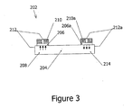
- the transport of spin polarized carriers is further explained by reference to Figure 3 , in which, there is shown an apparatus for producing spin polarized electrons, generally indicated as 202.
- the apparatus 202 comprises a layer 204 of semiconductor material, such as that shown in Figure 2 and described hereinbefore.
- a layer 206 of tunneling barrier material is deposited on the upper surface of the layer 204 of semiconductor material at one edge portion 208 of the semiconductor material.
- the layer 206 of tunneling barrier material is preferably magnesium oxide or aluminium oxide, having a thickness of from 0.5 to 5 nm.
- a layer 210 of ferromagnetic material is deposited on the layer 206 of tunneling barrier material.
- An electrical connection 212 is represented to show the completed circuit between the semiconductor material and the ferromagnetic material.
- a corresponding assembly is present on the opposite edge portion 214 of the semiconductor material 208, with identical components indicated using the same reference numerals and the suffix 'a'.
- An electric field is applied to the layer 204 of semiconductor material, inducing spin polarization of electrons in the material by way of the SHE.
- the spin polarization of the electrons in the first edge portion 208 is up, indicated by the symbol ⁇ in Figure 3 .
- electrons in the second edge portion 214 have the opposite, down orientation, indicated by the symbol ⁇ in Figure 3 .
- the layers 210 and 210a of ferromagnetic material have an intrinsic spin polarization of the carriers, the orientation of which is shown by the up arrow symbol to indicate that the orientation of the magnetic field in the ferromagnetic material corresponds to the ⁇ spin polarized electrons in the semiconductor.
- the orientation of the spin polarization is induced by the application of a magnetic field to the ferromagnetic material and may be varied by applying a differently oriented magnetic field.
- ⁇ spin polarized electrons may thus be produced and provided to the circuit 212 for use in external spintronics devices.
- the spin orientation of the ferromagnetic material is not aligned with the spin orientation of the electrons in the second edge portion 214 of the semiconductor 204, the production of ⁇ spin polarized electrons into the ferromagnetic material 210a and the circuit 212a will not occur.
- Reversal of the spin orientation of the carriers in the ferromagnetic material, by a suitable applied magnetic field, will halt the transport of ⁇ spin polarized electrons from the first edge portion 208 of the semiconductor 204 and allow production of ⁇ spin polarized electrons from the second edge portion 214.
- manipulation of the applied magnetic field may be used to control the spin orientation of electrons produced from the semiconductor material.
- FIG. 4 there is shown an apparatus for detecting spin polarized electrons, generally indicated as 402.
- the apparatus comprises a strip 404 of subject material having edge portions 406 and 408.
- the upper surface 410 of the subject material is provided with a plurality of conductor contacts 412, distributed along each of the edges 406 and 408.
- Each conductor contact comprises a material that is superconducting under the appropriate applied conditions, typically reduced temperature and, in some cases, increased pressure.
- the apparatus as shown in Figure 4 further comprises a base layer 414.
- a device 416 for measuring the conductance of the conductor contact at the interface with the subject material is provided and shown schematically in Figure 4 .
- the measurement device 416 comprises a 4-point probe 418, extending between the contact 412 and the base layer 414, and a constant current source/meter 420, similarly connected.
- the measurement device 416 allows measurement of the current I and potential difference V between the contact 412 and the base layer 414, from which the conductance at the interface is determined using I/V or dl/dV.
- the construction of the apparatus 402 is shown in more detail in Figure 3 .
- the subject material is shown comprising three layers of semiconductor material.
- the upper layer 422 is a layer of n-GaAs of 2 ⁇ m thickness.
- the base layer 414 comprises an intermediate layer 124 of Al 0.4 Ga 0.6 As of 2 ⁇ m thickness immediately adjacent and in contact with the upper layer 422.
- a support layer 426 of i-GaAs is provided.
- the conductor contacts 412 are formed of niobium, a Type 2 superconductor, having a T c of 9.25 K at atmospheric pressure.
- the measurement device 416 for measuring the conductance of the conductor contact 412 is connected across the conductor contact 412 and the intermediate layer 424 at the edge 406.
- the conductance of the conductor contact under superconducting conditions is determined.
- An electric field E is applied to the apparatus, represented by the arrow 430, in Figure 4 inducing a flow of electrons through the subject material 404.
- a second value of the conductance of the conductor contact is determined, again under superconducting conditions.
- the spin polarization of electrons across the subject material perpendicular to the applied electric field E is determined by a comparison of the first and second values of conductance. As described hereinbefore, polarization of the electrons according to their spin will suppress the conductance of the superconductor at the interface of the conductor contact and the upper layer 422. A spin polarization of 100% will suppress the conductance of the superconductor, according to the principles of Andreev Reflection known in the art and described hereinbefore.
Landscapes
- Physics & Mathematics (AREA)
- Condensed Matter Physics & Semiconductors (AREA)
- General Physics & Mathematics (AREA)
- Nanotechnology (AREA)
- Engineering & Computer Science (AREA)
- Chemical & Material Sciences (AREA)
- Crystallography & Structural Chemistry (AREA)
- Hall/Mr Elements (AREA)
- Photoreceptors In Electrophotography (AREA)
- Investigating, Analyzing Materials By Fluorescence Or Luminescence (AREA)
- Variable-Direction Aerials And Aerial Arrays (AREA)
- Investigating Or Analyzing Materials By The Use Of Magnetic Means (AREA)
- Measuring Magnetic Variables (AREA)
Claims (10)
- Procédé pour la production de vecteurs à spin polarisé à partir d'un matériau sujet, le procédé consistant à :appliquer une différence de potentiel à travers le matériau sujet (104, 204) entraînant la circulation d'un courant électrique à travers le matériau, induisant ainsi une polarisation des vecteurs à l'intérieur du matériau dans une direction perpendiculaire à la direction de circulation du courant, des vecteurs d'une orientation du spin se concentrant au niveau d'un premier bord du matériau sujet et des vecteurs de l'orientation opposée se concentrant au niveau d'un second bord du matériau, en face du premier bord sous l'action de l'effet Hall de spin (EHS) ; etplacer un matériau ferromagnétique (110, 210) en contact avec le matériau sujet (104, 204) pour permettre l'effet tunnel de spin de vecteurs à partir du matériau sujet dans le matériau ferromagnétique dans au moins une partie adjacente à l'un des premier ou second bords du matériau sujet ;caractérisé en ce quel'orientation du spin des vecteurs dans le matériau ferromagnétique (104, 204) est telle qu'elle entraîne le transport de vecteurs à spin polarisé à partir du matériau sujet dans le matériau ferromagnétique (110, 210), produisant ainsi un courant avec un degré de polarisation de spin pour l'utilisation dans des éléments spintroniques (212).
- Procédé selon la revendication 1, où le champ électrique appliqué au matériau sujet (104, 204) est de l'ordre de à 250 mV/µm au maximum, mieux encore de 0 à 100 mV/µm.
- Procédé selon une quelconque revendication précédente, où une injection de spin est réalisée par effet tunnel de spin.
- Procédé selon une quelconque revendication précédente, où l'orientation d'un champ magnétique appliqué au matériau ferromagnétique (110, 210) est ajustée pour déterminer l'orientation du spin de vecteurs à spin polarisé dans la partie du matériau sujet.
- Procédé selon une quelconque revendication précédente, où les vecteurs à spin polarisé sont injectés directement à partir du matériau ferromagnétique (110, 210) dans le matériau sujet (104, 204) ou où les vecteurs à spin polarisé sont injectés dans le matériau sujet à partir du matériau ferromagnétique à travers une couche barrière tunnel, la couche barrière tunnel comprenant de préférence un oxyde métallique, en particulier un oxyde de magnésium, aluminium ou hafnium.
- Appareil pour la production de vecteurs à spin polarisé dans un matériau sujet, l'appareil comprenant :un matériau sujet (104, 204) ;des moyens pour appliquer un champ électrique au matériau sujet (104, 204) de manière à induire la circulation d'un courant à travers le matériau sujet, induisant ainsi une polarisation de spin de vecteurs au niveau des premier et second bords opposés du matériau sujet dans une direction perpendiculaire au champ électrique sous l'action de l'effet Hall de spin (EHS) ; etun matériau ferromagnétique (110, 210) en contact avec au moins une partie adjacente à l'un des premier ou second bords du matériau sujet pour permettre l'effet tunnel de spin de vecteurs à partir du matériau sujet dans le matériau ferromagnétique;caractérisé en ce que l'appareil est configuré de telle manière àentraîner le déplacement de vecteurs à spin polarisé à partir du matériau sujet dans le matériau ferromagnétique et leur production pour l'utilisation dans un élément spintronique (212).
- Appareil selon la revendication 6, où le matériau sujet (104, 204) est un matériau semi-conducteur, le matériau semi-conducteur comprenant de préférence un semi-conducteur intrinsèque et/ou un semi-conducteur extrinsèque, le matériau semi-conducteur extrinsèque comprenant de préférence un semi-conducteur de type n et/ou de type p, le matériau sujet comprenant de préférence un semi-conducteur d'arséniure de gallium et/ou un semi-conducteur d'arséniure de gallium d'aluminium, avec Al0,4Ga0,6As comme arséniure de gallium d'aluminium préféré.
- Appareil selon la revendication 6 ou 7, où le matériau sujet (104, 204) comprend une pluralité de couches de différents matériaux, de préférence deux ou trois couches de matériau, mieux encore trois couches, chaque couche comprenant un différent matériau semi-conducteur.
- Appareil selon une quelconque des revendications 6 à 8, où le matériau ferromagnétique (110, 210) est un matériau cristallin ou un matériau amorphe, de préférence où le matériau ferromagnétique est sélectionné à partir de cobalt, fer, nickel, gadolinium, dysprosium, un oxyde mélangé de fer, nickel/fer, cuivre/fer, magnésium/fer, manganèse/fer, yttrium/fer, oxyde de chrome, oxyde d'europium, ou une combinaison sélectionnée à partir de manganèse/bismuth, manganèse/antimoine, nickel/manganèse/antimoine et manganèse/arsenic.
- Appareil selon une quelconque des revendications 6 à 9, où le matériau ferromagnétique (110, 210) est en contact avec le matériau sujet ou où une couche barrière tunnel (108, 206) est disposée entre le matériau ferromagnétique et le matériau sujet (104, 204), la couche barrière tunnel comprenant de préférence un oxyde métallique, où l'oxyde métallique est de préférence un oxyde de magnésium, aluminium, ou hafnium.
Applications Claiming Priority (3)
| Application Number | Priority Date | Filing Date | Title |
|---|---|---|---|
| GB0619980A GB2445377B (en) | 2006-10-10 | 2006-10-10 | Method of detecting electron spin polarisation and apparatus for the same |
| GB0619978A GB2442752B (en) | 2006-10-10 | 2006-10-10 | Method for detecting carrier spin polarisation and apparatus for the same |
| PCT/GB2007/003830 WO2008044001A2 (fr) | 2006-10-10 | 2007-10-09 | Procédé et appareil de détection de la polarisation en spin des porteurs |
Publications (2)
| Publication Number | Publication Date |
|---|---|
| EP2087366A2 EP2087366A2 (fr) | 2009-08-12 |
| EP2087366B1 true EP2087366B1 (fr) | 2010-12-22 |
Family
ID=39274915
Family Applications (1)
| Application Number | Title | Priority Date | Filing Date |
|---|---|---|---|
| EP07824084A Not-in-force EP2087366B1 (fr) | 2006-10-10 | 2007-10-09 | Procédé et appareil de détection de la polarisation en spin des porteurs |
Country Status (5)
| Country | Link |
|---|---|
| US (1) | US8093897B2 (fr) |
| EP (1) | EP2087366B1 (fr) |
| AT (1) | ATE492820T1 (fr) |
| DE (1) | DE602007011491D1 (fr) |
| WO (1) | WO2008044001A2 (fr) |
Cited By (1)
| Publication number | Priority date | Publication date | Assignee | Title |
|---|---|---|---|---|
| WO2014036510A1 (fr) * | 2012-09-01 | 2014-03-06 | Purdue Research Foundation | Commutateur de spin non volatil |
Families Citing this family (18)
| Publication number | Priority date | Publication date | Assignee | Title |
|---|---|---|---|---|
| KR100982660B1 (ko) * | 2008-08-01 | 2010-09-17 | 한국과학기술연구원 | 스핀 홀 효과를 이용한 자기메모리셀 판독 방법 및자기메모리 장치 |
| JP5202450B2 (ja) * | 2008-08-06 | 2013-06-05 | 株式会社日立製作所 | 局所磁界発生デバイス、磁界センサ、及び磁気ヘッド |
| US8300356B2 (en) * | 2010-05-11 | 2012-10-30 | Headway Technologies, Inc. | CoFe/Ni Multilayer film with perpendicular anistropy for microwave assisted magnetic recording |
| JP5590488B2 (ja) * | 2010-08-27 | 2014-09-17 | 独立行政法人理化学研究所 | 電流−スピン流変換素子 |
| EP2800970B1 (fr) | 2012-01-04 | 2016-09-28 | Magnomics, S.A. | Dispositif monolithique combinant des capteurs cmos et magnétorésistifs |
| WO2013122024A1 (fr) * | 2012-02-14 | 2013-08-22 | Tdk株式会社 | Structure d'électrode pour implantation de spin et élément de transport de spin utilisant celle-ci |
| EP2688072B1 (fr) * | 2012-07-19 | 2014-06-18 | Forschungsverbund Berlin e.V. | Circuit spintronique et procédé de fonctionnement associé |
| CN103968948B (zh) * | 2013-02-04 | 2016-04-27 | 清华大学 | 偏振光的检测方法 |
| CN103968949B (zh) * | 2013-02-04 | 2016-04-27 | 清华大学 | 偏振光检测系统 |
| US9099119B2 (en) | 2013-02-11 | 2015-08-04 | HGST Netherlands B.V. | Magnetic read sensor using spin hall effect |
| US8889433B2 (en) | 2013-03-15 | 2014-11-18 | International Business Machines Corporation | Spin hall effect assisted spin transfer torque magnetic random access memory |
| CN103809101A (zh) * | 2014-02-13 | 2014-05-21 | 中国科学院半导体研究所 | 光致反常霍尔效应的变温测量装置及测量方法 |
| FR3021176B1 (fr) * | 2014-05-15 | 2016-07-01 | Thales Sa | Circuit logique a base de vannes de spin du type a supercourant polarise en spin et circuit integrant de telles porte logiques |
| US9269415B1 (en) | 2014-09-18 | 2016-02-23 | International Business Machines Corporation | Utilization of the anomalous hall effect or polarized spin hall effect for MRAM applications |
| CN105717467B (zh) * | 2016-03-01 | 2019-03-29 | 中国科学院半导体研究所 | 铁磁半导体平面内磁各向异性的光电流测试系统及方法 |
| US20210126181A1 (en) * | 2019-10-24 | 2021-04-29 | Microsoft Technology Licensing, Llc | Semiconductor-superconductor hybrid device, its manufacture and uses |
| US12082512B2 (en) | 2019-10-24 | 2024-09-03 | Microsoft Technology Licensing, Llc | Semiconductor-superconductor hybrid device |
| US11946890B2 (en) * | 2021-05-24 | 2024-04-02 | Kla Corporation | Method for measuring high resistivity test samples using voltages or resistances of spacings between contact probes |
Family Cites Families (5)
| Publication number | Priority date | Publication date | Assignee | Title |
|---|---|---|---|---|
| US6403999B1 (en) * | 2000-05-23 | 2002-06-11 | Spinix Corporation | Detection of polarized spin transport in semiconductors |
| US7309903B2 (en) * | 2002-03-26 | 2007-12-18 | Japan Science And Technology Agency | Tunneling magnetoresistance device semiconductor junction device magnetic memory and semiconductor light-emitting device |
| JP4714918B2 (ja) * | 2002-11-29 | 2011-07-06 | 独立行政法人科学技術振興機構 | スピン注入素子及びスピン注入素子を用いた磁気装置 |
| EP1548702A1 (fr) * | 2003-12-24 | 2005-06-29 | Interuniversitair Microelektronica Centrum Vzw | Procédé de réglage ultrarapide d'une cellule magnétique et dispositifs associés |
| KR101093776B1 (ko) * | 2010-01-21 | 2011-12-19 | 충남대학교산학협력단 | 자기 센서 |
-
2007
- 2007-10-09 DE DE602007011491T patent/DE602007011491D1/de active Active
- 2007-10-09 US US12/445,175 patent/US8093897B2/en not_active Expired - Fee Related
- 2007-10-09 AT AT07824084T patent/ATE492820T1/de not_active IP Right Cessation
- 2007-10-09 EP EP07824084A patent/EP2087366B1/fr not_active Not-in-force
- 2007-10-09 WO PCT/GB2007/003830 patent/WO2008044001A2/fr not_active Ceased
Cited By (1)
| Publication number | Priority date | Publication date | Assignee | Title |
|---|---|---|---|---|
| WO2014036510A1 (fr) * | 2012-09-01 | 2014-03-06 | Purdue Research Foundation | Commutateur de spin non volatil |
Also Published As
| Publication number | Publication date |
|---|---|
| EP2087366A2 (fr) | 2009-08-12 |
| WO2008044001A3 (fr) | 2008-10-02 |
| US20100072993A1 (en) | 2010-03-25 |
| WO2008044001A2 (fr) | 2008-04-17 |
| US8093897B2 (en) | 2012-01-10 |
| ATE492820T1 (de) | 2011-01-15 |
| DE602007011491D1 (de) | 2011-02-03 |
Similar Documents
| Publication | Publication Date | Title |
|---|---|---|
| EP2087366B1 (fr) | Procédé et appareil de détection de la polarisation en spin des porteurs | |
| Jedema et al. | Electrical spin injection and accumulation at room temperature in an all-metal mesoscopic spin valve | |
| Žutić et al. | Spintronics: Fundamentals and applications | |
| Pu et al. | Mott Relation for Anomalous Hall and Nernst Effects<? format?> in Ga 1-x Mn x As Ferromagnetic Semiconductors | |
| Schmidt et al. | Large magnetoresistance effect due to spin injection into a nonmagnetic semiconductor | |
| Moodera et al. | Spin-tunneling in ferromagnetic junctions | |
| Pena et al. | Giant magnetoresistance in ferromagnet/superconductor superlattices | |
| Qu et al. | Intrinsic spin Seebeck effect in Au/YIG | |
| Chun et al. | Spin-polarized tunneling in hybrid metal-semiconductor magnetic tunnel junctions | |
| KR100678758B1 (ko) | 스핀주입 소자 및 스핀주입 소자를 이용한 자기 장치 | |
| Giddings et al. | Large tunneling anisotropic magnetoresistance in (Ga, Mn) As nanoconstrictions | |
| EP0524369A2 (fr) | Dispositif nouveau pour la magnétisation sélective et méthode | |
| Gim et al. | Current injection into high temperature superconductors: Does spin matter? | |
| CN100390561C (zh) | 具半磁性连接的半导体组件 | |
| Schmidt et al. | Dilute magnetic semiconductors in spin-polarized electronics | |
| GB2479893A (en) | Spin field effect transistor | |
| Jara et al. | Bias current dependence of superconducting transition temperature in superconducting spin-valve nanowires | |
| GB2442752A (en) | Analysis of carrier spin polarisation using the Spin Hall Effect | |
| Okuma et al. | Vortex phase diagram and quantum fluctuations in thick a− Mo x Si 1− x films | |
| Wang et al. | Increase of nonlocal spin signal at high dc bias due to a redistribution of the injection current | |
| Takahashi et al. | Spin injection and transport in magnetic nanostructures | |
| Ishikura et al. | Electrical spin injection from ferromagnet into an InAs quantum well through a MgO tunnel barrier | |
| GB2445377A (en) | Electron spin polarization detection in semiconductor materials | |
| Tokuda et al. | Spin transport measurements in metallic Bi/Ni nanowires | |
| Vignale | Observing the spin Coulomb drag in spin-valve devices |
Legal Events
| Date | Code | Title | Description |
|---|---|---|---|
| PUAI | Public reference made under article 153(3) epc to a published international application that has entered the european phase |
Free format text: ORIGINAL CODE: 0009012 |
|
| 17P | Request for examination filed |
Effective date: 20090414 |
|
| AK | Designated contracting states |
Kind code of ref document: A2 Designated state(s): AT BE BG CH CY CZ DE DK EE ES FI FR GB GR HU IE IS IT LI LT LU LV MC MT NL PL PT RO SE SI SK TR |
|
| 17Q | First examination report despatched |
Effective date: 20091009 |
|
| DAX | Request for extension of the european patent (deleted) | ||
| GRAP | Despatch of communication of intention to grant a patent |
Free format text: ORIGINAL CODE: EPIDOSNIGR1 |
|
| GRAS | Grant fee paid |
Free format text: ORIGINAL CODE: EPIDOSNIGR3 |
|
| GRAA | (expected) grant |
Free format text: ORIGINAL CODE: 0009210 |
|
| AK | Designated contracting states |
Kind code of ref document: B1 Designated state(s): AT BE BG CH CY CZ DE DK EE ES FI FR GB GR HU IE IS IT LI LT LU LV MC MT NL PL PT RO SE SI SK TR |
|
| REG | Reference to a national code |
Ref country code: GB Ref legal event code: FG4D |
|
| REG | Reference to a national code |
Ref country code: CH Ref legal event code: EP |
|
| REG | Reference to a national code |
Ref country code: IE Ref legal event code: FG4D |
|
| REF | Corresponds to: |
Ref document number: 602007011491 Country of ref document: DE Date of ref document: 20110203 Kind code of ref document: P |
|
| REG | Reference to a national code |
Ref country code: DE Ref legal event code: R096 Ref document number: 602007011491 Country of ref document: DE Effective date: 20110203 |
|
| REG | Reference to a national code |
Ref country code: NL Ref legal event code: VDEP Effective date: 20101222 |
|
| PG25 | Lapsed in a contracting state [announced via postgrant information from national office to epo] |
Ref country code: LT Free format text: LAPSE BECAUSE OF FAILURE TO SUBMIT A TRANSLATION OF THE DESCRIPTION OR TO PAY THE FEE WITHIN THE PRESCRIBED TIME-LIMIT Effective date: 20101222 |
|
| LTIE | Lt: invalidation of european patent or patent extension |
Effective date: 20101222 |
|
| PG25 | Lapsed in a contracting state [announced via postgrant information from national office to epo] |
Ref country code: FI Free format text: LAPSE BECAUSE OF FAILURE TO SUBMIT A TRANSLATION OF THE DESCRIPTION OR TO PAY THE FEE WITHIN THE PRESCRIBED TIME-LIMIT Effective date: 20101222 Ref country code: AT Free format text: LAPSE BECAUSE OF FAILURE TO SUBMIT A TRANSLATION OF THE DESCRIPTION OR TO PAY THE FEE WITHIN THE PRESCRIBED TIME-LIMIT Effective date: 20101222 Ref country code: LV Free format text: LAPSE BECAUSE OF FAILURE TO SUBMIT A TRANSLATION OF THE DESCRIPTION OR TO PAY THE FEE WITHIN THE PRESCRIBED TIME-LIMIT Effective date: 20101222 Ref country code: BG Free format text: LAPSE BECAUSE OF FAILURE TO SUBMIT A TRANSLATION OF THE DESCRIPTION OR TO PAY THE FEE WITHIN THE PRESCRIBED TIME-LIMIT Effective date: 20110322 Ref country code: CY Free format text: LAPSE BECAUSE OF FAILURE TO SUBMIT A TRANSLATION OF THE DESCRIPTION OR TO PAY THE FEE WITHIN THE PRESCRIBED TIME-LIMIT Effective date: 20101222 Ref country code: SI Free format text: LAPSE BECAUSE OF FAILURE TO SUBMIT A TRANSLATION OF THE DESCRIPTION OR TO PAY THE FEE WITHIN THE PRESCRIBED TIME-LIMIT Effective date: 20101222 Ref country code: SE Free format text: LAPSE BECAUSE OF FAILURE TO SUBMIT A TRANSLATION OF THE DESCRIPTION OR TO PAY THE FEE WITHIN THE PRESCRIBED TIME-LIMIT Effective date: 20101222 |
|
| PG25 | Lapsed in a contracting state [announced via postgrant information from national office to epo] |
Ref country code: CZ Free format text: LAPSE BECAUSE OF FAILURE TO SUBMIT A TRANSLATION OF THE DESCRIPTION OR TO PAY THE FEE WITHIN THE PRESCRIBED TIME-LIMIT Effective date: 20101222 Ref country code: ES Free format text: LAPSE BECAUSE OF FAILURE TO SUBMIT A TRANSLATION OF THE DESCRIPTION OR TO PAY THE FEE WITHIN THE PRESCRIBED TIME-LIMIT Effective date: 20110402 Ref country code: GR Free format text: LAPSE BECAUSE OF FAILURE TO SUBMIT A TRANSLATION OF THE DESCRIPTION OR TO PAY THE FEE WITHIN THE PRESCRIBED TIME-LIMIT Effective date: 20110323 Ref country code: IS Free format text: LAPSE BECAUSE OF FAILURE TO SUBMIT A TRANSLATION OF THE DESCRIPTION OR TO PAY THE FEE WITHIN THE PRESCRIBED TIME-LIMIT Effective date: 20110422 Ref country code: EE Free format text: LAPSE BECAUSE OF FAILURE TO SUBMIT A TRANSLATION OF THE DESCRIPTION OR TO PAY THE FEE WITHIN THE PRESCRIBED TIME-LIMIT Effective date: 20101222 Ref country code: PT Free format text: LAPSE BECAUSE OF FAILURE TO SUBMIT A TRANSLATION OF THE DESCRIPTION OR TO PAY THE FEE WITHIN THE PRESCRIBED TIME-LIMIT Effective date: 20110422 Ref country code: BE Free format text: LAPSE BECAUSE OF FAILURE TO SUBMIT A TRANSLATION OF THE DESCRIPTION OR TO PAY THE FEE WITHIN THE PRESCRIBED TIME-LIMIT Effective date: 20101222 |
|
| PG25 | Lapsed in a contracting state [announced via postgrant information from national office to epo] |
Ref country code: RO Free format text: LAPSE BECAUSE OF FAILURE TO SUBMIT A TRANSLATION OF THE DESCRIPTION OR TO PAY THE FEE WITHIN THE PRESCRIBED TIME-LIMIT Effective date: 20101222 Ref country code: PL Free format text: LAPSE BECAUSE OF FAILURE TO SUBMIT A TRANSLATION OF THE DESCRIPTION OR TO PAY THE FEE WITHIN THE PRESCRIBED TIME-LIMIT Effective date: 20101222 Ref country code: SK Free format text: LAPSE BECAUSE OF FAILURE TO SUBMIT A TRANSLATION OF THE DESCRIPTION OR TO PAY THE FEE WITHIN THE PRESCRIBED TIME-LIMIT Effective date: 20101222 Ref country code: NL Free format text: LAPSE BECAUSE OF FAILURE TO SUBMIT A TRANSLATION OF THE DESCRIPTION OR TO PAY THE FEE WITHIN THE PRESCRIBED TIME-LIMIT Effective date: 20101222 |
|
| PLBE | No opposition filed within time limit |
Free format text: ORIGINAL CODE: 0009261 |
|
| STAA | Information on the status of an ep patent application or granted ep patent |
Free format text: STATUS: NO OPPOSITION FILED WITHIN TIME LIMIT |
|
| PG25 | Lapsed in a contracting state [announced via postgrant information from national office to epo] |
Ref country code: DK Free format text: LAPSE BECAUSE OF FAILURE TO SUBMIT A TRANSLATION OF THE DESCRIPTION OR TO PAY THE FEE WITHIN THE PRESCRIBED TIME-LIMIT Effective date: 20101222 |
|
| 26N | No opposition filed |
Effective date: 20110923 |
|
| PG25 | Lapsed in a contracting state [announced via postgrant information from national office to epo] |
Ref country code: IT Free format text: LAPSE BECAUSE OF FAILURE TO SUBMIT A TRANSLATION OF THE DESCRIPTION OR TO PAY THE FEE WITHIN THE PRESCRIBED TIME-LIMIT Effective date: 20101222 |
|
| REG | Reference to a national code |
Ref country code: DE Ref legal event code: R097 Ref document number: 602007011491 Country of ref document: DE Effective date: 20110923 |
|
| PG25 | Lapsed in a contracting state [announced via postgrant information from national office to epo] |
Ref country code: MC Free format text: LAPSE BECAUSE OF NON-PAYMENT OF DUE FEES Effective date: 20111031 |
|
| REG | Reference to a national code |
Ref country code: CH Ref legal event code: PL |
|
| GBPC | Gb: european patent ceased through non-payment of renewal fee |
Effective date: 20111009 |
|
| REG | Reference to a national code |
Ref country code: FR Ref legal event code: ST Effective date: 20120629 |
|
| PG25 | Lapsed in a contracting state [announced via postgrant information from national office to epo] |
Ref country code: LI Free format text: LAPSE BECAUSE OF NON-PAYMENT OF DUE FEES Effective date: 20111031 Ref country code: CH Free format text: LAPSE BECAUSE OF NON-PAYMENT OF DUE FEES Effective date: 20111031 Ref country code: DE Free format text: LAPSE BECAUSE OF NON-PAYMENT OF DUE FEES Effective date: 20120501 |
|
| REG | Reference to a national code |
Ref country code: IE Ref legal event code: MM4A |
|
| REG | Reference to a national code |
Ref country code: DE Ref legal event code: R119 Ref document number: 602007011491 Country of ref document: DE Effective date: 20120501 |
|
| PG25 | Lapsed in a contracting state [announced via postgrant information from national office to epo] |
Ref country code: FR Free format text: LAPSE BECAUSE OF NON-PAYMENT OF DUE FEES Effective date: 20111102 Ref country code: GB Free format text: LAPSE BECAUSE OF NON-PAYMENT OF DUE FEES Effective date: 20111009 |
|
| PG25 | Lapsed in a contracting state [announced via postgrant information from national office to epo] |
Ref country code: IE Free format text: LAPSE BECAUSE OF NON-PAYMENT OF DUE FEES Effective date: 20111009 |
|
| PG25 | Lapsed in a contracting state [announced via postgrant information from national office to epo] |
Ref country code: MT Free format text: LAPSE BECAUSE OF FAILURE TO SUBMIT A TRANSLATION OF THE DESCRIPTION OR TO PAY THE FEE WITHIN THE PRESCRIBED TIME-LIMIT Effective date: 20101222 |
|
| PG25 | Lapsed in a contracting state [announced via postgrant information from national office to epo] |
Ref country code: LU Free format text: LAPSE BECAUSE OF NON-PAYMENT OF DUE FEES Effective date: 20111009 |
|
| PG25 | Lapsed in a contracting state [announced via postgrant information from national office to epo] |
Ref country code: TR Free format text: LAPSE BECAUSE OF FAILURE TO SUBMIT A TRANSLATION OF THE DESCRIPTION OR TO PAY THE FEE WITHIN THE PRESCRIBED TIME-LIMIT Effective date: 20101222 |
|
| PG25 | Lapsed in a contracting state [announced via postgrant information from national office to epo] |
Ref country code: HU Free format text: LAPSE BECAUSE OF FAILURE TO SUBMIT A TRANSLATION OF THE DESCRIPTION OR TO PAY THE FEE WITHIN THE PRESCRIBED TIME-LIMIT Effective date: 20101222 |