EP2088512B1 - Speichersystem - Google Patents
Speichersystem Download PDFInfo
- Publication number
- EP2088512B1 EP2088512B1 EP07832620A EP07832620A EP2088512B1 EP 2088512 B1 EP2088512 B1 EP 2088512B1 EP 07832620 A EP07832620 A EP 07832620A EP 07832620 A EP07832620 A EP 07832620A EP 2088512 B1 EP2088512 B1 EP 2088512B1
- Authority
- EP
- European Patent Office
- Prior art keywords
- memory
- amount
- writing
- erase operations
- exhaustion level
- Prior art date
- Legal status (The legal status is an assumption and is not a legal conclusion. Google has not performed a legal analysis and makes no representation as to the accuracy of the status listed.)
- Active
Links
Images


Classifications
-
- G—PHYSICS
- G06—COMPUTING OR CALCULATING; COUNTING
- G06F—ELECTRIC DIGITAL DATA PROCESSING
- G06F12/00—Accessing, addressing or allocating within memory systems or architectures
- G06F12/16—Protection against loss of memory contents
-
- G—PHYSICS
- G11—INFORMATION STORAGE
- G11C—STATIC STORES
- G11C16/00—Erasable programmable read-only memories
- G11C16/02—Erasable programmable read-only memories electrically programmable
- G11C16/06—Auxiliary circuits, e.g. for writing into memory
- G11C16/34—Determination of programming status, e.g. threshold voltage, overprogramming or underprogramming, retention
- G11C16/349—Arrangements for evaluating degradation, retention or wearout, e.g. by counting erase cycles
-
- G—PHYSICS
- G06—COMPUTING OR CALCULATING; COUNTING
- G06F—ELECTRIC DIGITAL DATA PROCESSING
- G06F11/00—Error detection; Error correction; Monitoring
- G06F11/008—Reliability or availability analysis
-
- G—PHYSICS
- G06—COMPUTING OR CALCULATING; COUNTING
- G06F—ELECTRIC DIGITAL DATA PROCESSING
- G06F11/00—Error detection; Error correction; Monitoring
- G06F11/07—Responding to the occurrence of a fault, e.g. fault tolerance
- G06F11/08—Error detection or correction by redundancy in data representation, e.g. by using checking codes
- G06F11/10—Adding special bits or symbols to the coded information, e.g. parity check, casting out 9's or 11's
- G06F11/1008—Adding special bits or symbols to the coded information, e.g. parity check, casting out 9's or 11's in individual solid state devices
- G06F11/1068—Adding special bits or symbols to the coded information, e.g. parity check, casting out 9's or 11's in individual solid state devices in sector programmable memories, e.g. flash disk
-
- G—PHYSICS
- G06—COMPUTING OR CALCULATING; COUNTING
- G06F—ELECTRIC DIGITAL DATA PROCESSING
- G06F12/00—Accessing, addressing or allocating within memory systems or architectures
-
- G—PHYSICS
- G11—INFORMATION STORAGE
- G11C—STATIC STORES
- G11C16/00—Erasable programmable read-only memories
- G11C16/02—Erasable programmable read-only memories electrically programmable
Definitions
- the present invention relates to a memory system.
- a flash memory has such characteristics that data is not erased even if it is powered off, and it has a structure suitable for high integration, and used in information apparatuses such as a mobile phone and a digital camera.
- Types of Flash EEPROM nonvolatile memory are mainly an NOR type and an NAND type.
- NOR type a read rate is high, the number of read operations is about 10 13 , and it is used as an instruction code storage.
- the NOR type has a small effective bandwidth for writing, and therefore not suitable for file recording.
- NAND type although an access rate is low compared to the NOR type, high integration is allowed, a large number of bits can be stored or erased at the same time is large, and written data can be captured in burst and programming is allowed in page units having many bits.
- the NAND type memory has a large effective bandwidth, and is used for a memory card, a USB memory, a memory of a mobile phone, a memory of a portable music player, and the like. Recently, it is also considered as a replacement of a hard disk (hereinafter referred to as an HDD).
- an HDD hard disk
- An HDD is equipped with a Self-Monitoring, Analysis and Reporting Technology (commonly known as SMART), which is a self-diagnosis function intended for early detection of a failure of the HDD itself and failure prediction, and thereby can notify a user of failure rate.
- SMART Self-Monitoring, Analysis and Reporting Technology
- Many of currently manufactured HDDs have this SMART, and predict a failure rate from items including a temperature, an operating time, a spin-up time, the number of alternate sectors (spare areas in which a sector causing bad data is arranged), and the like.
- an NAND type flash memory is also considered to need reliability equivalent to HDDs, it requires a self-diagnosis function like SMART.
- reason of failure in the NAND type flash memory is different from that of the HDDs. Due to characteristics of recoding media of HDDs, they have no limit on the number of write operations, but is susceptible to heat. Further, since they are machine components, there is a problem of aged deterioration of mechanical operation. On the other hand, the NAND type flash memory has little machine components, but consideration should be given to a failure caused by bad data due to an excessive number of store/erase operations. Therefore, a new criterion of system lifetime is needed in consideration of the number of store/erase operations specific to the NAND type flash memory.
- a limit on the number of store/erase operations of the NAND type flash memory will be described.
- high voltage is applied between a substrate and a gate such that electrons are injected and released into a floating gate. If this is performed many times, gate oxide film around the floating gate is deteriorated, and if it is left as is for a long time, the electrons injected into the floating gate get out therefrom, and data is destroyed. In other words, as the number of write operations increases, retention characteristics degrade.
- the number of write operations of current flash memories is about 10 5 , which is less than that of other nonvolatile memories.
- wear leveling is performed in which the number of erase operations is counted and a threshold value is set for each block, and physical address translation is performed between a block whose number of erase operations is large and a block whose number of erase operations is small, so that the numbers of store/erase operations are averaged.
- a storage device which determines a memory state of a flash memory or the like, including: a memory having a main memory area and a spare memory area; display means; and processing means, wherein, when the number of rewrite operations in each address of the main memory area reaches a specified number, information stored in the address is transferred to the spare memory area; and when a remaining capacity of the spare memory area reaches a specified remaining capacity, the display means is driven to notify an operator or the like of a time to replace the memory (see, for example, Japanese Patent Laid-Open No. 2000-181805 ).
- an end of memory lifetime for writing is determined to be reached and the memory is replaced in a state where the number of write operations in the spare memory area is still small. Therefore, the memory cannot be efficiently used.
- US-B1-6,249,838 discloses data storage unit, such as flash memory, nonvolatile random access memory and like, with information stored therein, or physically coupled thereto, which indicates, or can be used to determine, remaining or impending end of lifetime of the data storage unit or its components.
- data storage unit such as flash memory, nonvolatile random access memory and like
- a counter initialized to the number of maximum permissible flash memory erasures is stored in a counter, such as in the header portion of the flash memory. The counter is decremented with each erasure and, as the counter approaches zero, appropriate actions can be taken such as warning the user, support personnel, vendor and the like and/or disabling the flash memory.
- US-A1-2006/0265545 discloses a judging unit for determining whether an accumulated rewrite count management table is in a flash memory. If the accumulated rewrite count management table is not in the flash memory, then a generating unit generates an accumulated rewrite count management table in the flash memory, and a recording unit records an accumulated rewrite count in the accumulated rewrite count management table which is generated. A monitoring unit monitors the lifetime of a storage device based on the accumulated rewrite count recorded in the accumulated rewrite count management table and a rewrite count limitative value recorded in the flash memory.
- US-B1-6,426,898 discloses a method of erasing memory cells in a flash memory device that recombines holes trapped in the tunnel oxide (after an erase operation) with electrons passing through the tunnel oxide is disclosed.
- the method uses an erase operation that over-erases all memory cells undergoing the erase operation.
- a cell healing operation is performed on the over-erased cells.
- the healing operation causes electrons to pass through the tunnel oxide and recombine with trapped holes.
- the recombination substantially reduces the trapped holes within the tunnel oxide without reducing the speed of the erase operation.
- by reducing trapped holes charge retention, overall performance and endurance of the flash memory cells are substantially increased.
- US-A1-2003/0078741 discloses a method and apparatus which periodically sense environmental conditions, such as temperature, humidity, or voltage applied to a product, and apply these sensed measurements to models of ageing acceleration. Acceleration factors from the models are accumulated in nonvolatile storage. The accumulated effective aging of the product is displayed to the owner or prospective customer in various desired formats, such as effective age, current acceleration factor, estimate of effective life used, or estimate of remaining life left in the product. A warning can be sent to the user to indicate that the product's effective life is over or is nearly over.
- WO-A1-2006/005661 discloses an electronic device with a microprocessor and a non-volatile data-recordable memory for a predetermined maximum number of write accesses, wherein said electronic device comprises a counter for a write access recording and the microprocessor generates an alarm signal according to development of the number of the write accesses and possibly of the maximum number of write accesses.
- US-A1-2003/0217323 discloses a data quality assessment method, where the quality of data stored in a memory system is assessed by different methods, and the memory system is operated according to the assessed quality.
- the data quality can be assessed during read operations.
- Subsequent use of an Error Correction Code can utilize the quality indications to detect and reconstruct the data with improved effectiveness.
- a statistics of data quality can be constructed and digital data values can be associated in a modified manner to prevent data corruption.
- the corrective actions can be implemented specifically on the poor quality data, according to suitably chosen schedules, and with improved effectiveness because of the knowledge provided by the quality indications.
- US-A1-2004/0158775 discloses a nonvolatile memory aimed to detect, notify, and save an abnormal area in semiconductor memory for greatly improving reliability.
- An inside of semiconductor memories provided for a memory card comprises a user area, a substitution area, an area substitution information storage area, and a management area.
- An inside of semiconductor memories comprises a user area, a substitution area, and a management area.
- the user area is a data area a user can use.
- the substitution area is substituted when an error occurs in the user area.
- the area substitution information storage area stores area substitution area information.
- the management area stores substitution information.
- the information processing section performs substitution on two levels as follows. When detecting an operation indicating a symptom of failure in a semiconductor memory area, the information processing section performs area substitution during an idle state of the memory card. When detecting a faulty operation in an area, the information processing section immediately performs area substitution.
- An object of the present invention is to provide a memory system which determines a memory state such as an exhaustion level and allows a memory to be efficiently used.
- a memory system includes: a first memory in which data can be electrically written/erased; a second memory arranged to monitor an amount of writing and an amount of reading with respect to the first memory, and retains the amount of writing, the amount of reading, and a limiting amount of writing based on a capacity of the first memory and a limiting number of write operations; and a controller which is connected to be given a self-diagnosis command from an outside through a connection interface, and which is arranged to retrieve the amount of writing, the amount of reading, and the limiting amount of writing from the second memory based on the self-diagnosis command and outputs the amount of writing, the amount of reading, and the limiting amount of writing to the outside through the connection interface.
- a memory state such as an exhaustion level can be determined, and a memory can be efficiently used.
- Fig. 1 shows a schematic configuration of a memory system according to the first background example for better understanding the present invention.
- the memory system includes an NAND type flash memory 1, a nonvolatile memory (FeRAM) 2, and a controller 3.
- the memory system is connected to a computer 4 through a connection interface 31 included in the controller 3.
- a display unit (display) 5 and a speaker 6 are connected to the computer 4.
- the FeRAM 2 has a counter (not shown), and for wear leveling, counts the number of erase operations in each block of the NAND type flash memory 1 as well as retaining a total of the number of erase operations. In addition, it retains a maximum number of erase operations and a threshold of exhaustion level of the NAND type flash memory 1. The exhaustion level will be described later.
- the maximum number of erase operations is obtained here from (limiting number of store/erase operations in each block of the NAND type flash memory 1) x (total number of blocks of the NAND type flash memory 1).
- FeRAM 2 also has a function as a cache for high-speed reading/writing of the NAND type flash memory 1.
- the controller 3 has the connection interface 31, a processing unit (MPU) 32, a FeRAM controller 33, and a memory controller 34.
- the FERAM controller 33 controls transferring data retained by the FeRAM 2
- the memory controller 34 controls transferring data to the NAND type flash memory 1.
- the memory controller 34 includes an error correction circuit (ECC) 35.
- ECC error correction circuit
- the memory controller 34 can detect this error and correct it to a correct value.
- wear leveling is performed such that the number of store/erase operations in each block is averaged.
- a self-diagnosis command is regularly issued from the computer 4 to this memory system.
- the processing unit 32 receives the self-diagnosis command through the connection interface 31, and performs control to output a total of the number of erase operations, a maximum number of erase operations, and a threshold of exhaustion level which are retained by the FeRAM 2 to the computer 4 through the connection interface 31.
- the computer 4 calculates an exhaustion level of the NAND type flash memory 1 based on the total of the number of erase operations and the maximum number of erase operations.
- the exhaustion level is a ratio of the total of the number of erase operations to the maximum number of erase operations.
- the exhaustion level and a backup alarm are displayed on the display unit 5 as shown in Fig. 3(a) so that a user is notified of them.
- the exhaustion level is calculated and displayed in percentage here.
- an alarm sound is emitted from the speaker 6 to give notification to the user.
- the user can optionally display the exhaustion level on the display unit 5. If the exhaustion level is less than or equal to the threshold, the exhaustion level is displayed as shown in Fig. 3(b) .
- various representations may be used as a notification to a user. For example, it goes without saying that a circle graph, a line graph, various words and colors, and other indications can be used.
- Fig. 4 shows a process flow of calculation of an exhaustion level of the NAND type flash memory 1 and notification of the exhaustion level to a user.
- Step S1 The processing unit 32 accepts a self-diagnosis command issued by the computer 4.
- Step S2 A total of the number of erase operations, the maximum number of erase operations, and a threshold of exhaustion level are retrieved from the FeRAM 2 and outputted to the computer 4.
- Step S3 The exhaustion level is calculated by the computer 4.
- Step S4 Whether or not the calculated exhaustion level is greater than the threshold is determined. If it is less than or equal to the threshold, the process is terminated. If it is greater than the threshold, the process proceeds to step S5.
- Step S5 A backup alarm sound is emitted from the speaker 6.
- Step S6 The exhaustion level and a backup alarm are displayed on the display unit 5.
- the step S5 of emitting an alarm sound and the step S6 of displaying an alarm may be replaced with each other.
- the exhaustion level is calculated from the total of the number of erase operations.
- an exhaustion level may be calculated from the number of erase operations in each block and a maximum number of erase operations.
- the numbers of rewrite operations are evenly distributed among blocks by wear leveling so that the number of rewrite operations with respect to a whole memory area is increased.
- a notification of an exhaustion level of the NAND type flash memory 1 can be provided to a user at any time. Backup is recommended when the exhaustion level exceeds a predetermined threshold and comes close to the end of a system lifetime, so that data loss can be prevented before it happens.
- a memory state such as an exhaustion level can be determined, and a memory can be efficiently used.
- Fig. 5 shows a schematic configuration of a memory system according to the second background example helpful for better understanding the present invention.
- This memory system is configured to further include a timer 7 in addition to the memory system of the first background example shown in Fig. 1 .
- the timer 7 measures an energization time of this memory system.
- the measured energization time is retained in the FeRAM 2.
- a self-diagnosis command is regularly issued from the computer 4 to this memory system.
- the processing unit 32 receives the self-diagnosis command through the connection interface 31, and performs control to output a total of the number of erase operations, a maximum number of erase operations, and an energization time, and a remaining lifetime which are retained by the FeRAM 2 to the computer 4 through the connection interface 31. The remaining lifetime will be described later.
- the computer 4 calculates an exhaustion level of the NAND type flash memory 1 based on the total of the number of erase operations and the maximum number of erase operations. Further, it calculates the remaining lifetime from the exhaustion level and the energization time.
- the exhaustion level is a ratio of the total of the number of erase operations to the maximum number of erase operations.
- the exhaustion level is calculated and displayed in percentage, and the remaining lifetime is calculated and displayed in units of days.
- an alarm sound may be emitted from the speaker 6 to give notification to the user.
- the user can optionally display the exhaustion level and the remaining lifetime on the display unit 5.
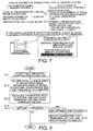
- Fig. 8 shows a process flow of calculation of an exhaustion level and a lifetime of the NAND type flash memory 1 and notification of them to a user.
- Step S11 The processing unit 32 accepts a self-diagnosis - command issued by the computer 4.
- Step S12 A total of the number of erase operations, the maximum number of erase operations, an energization time, and a threshold of a remaining lifetime are retrieved from the FeRAM 2 and outputted to the computer 4.
- Step S13 The exhaustion level and the remaining lifetime are calculated by the computer 4.
- Step S14 Whether or not the calculated remaining lifetime is less than the threshold is determined. If it is greater than or equal to the threshold, the process is terminated. If it is less than the threshold, the process proceeds to step S15.
- Step S15 A backup alarm sound is emitted from the speaker 6.
- Step S16 The exhaustion level, the remaining lifetime, and a backup alarm are displayed on the display unit 5.
- the exhaustion level is calculated from the total of the number of erase operations.
- an exhaustion level may be calculated from the number of erase operations in each block and a maximum number of erase operations.
- the numbers of rewrite operations are evenly distributed among blocks by wear leveling so that the number of rewrite operations with respect to a whole memory area is increased.
- a notification of an exhaustion level of the NAND type flash memory 1 can be provided to a user at any time. Backup is recommended when the exhaustion level exceeds a predetermined threshold and comes close to the end of a system lifetime, so that data loss can be prevented before it happens. Further, a remaining lifetime is displayed, so that the user can replace a memory system in an efficient way.
- a memory state such as a remaining lifetime can be determined, and a memory can be efficiently used.
- FIG. 9 shows a schematic configuration of a memory system according to the first embodiment of thepresent invention.
- the memory system has a configuration similar to the first background example shown in Fig. 1 .
- an exhaustion level is calculated from a maximum number of erase operations and a total of the number of erase operations.
- an exhaustion level is calculated from an amount of writing into the NAND type flash memory 1 and an amount of reading therefrom.
- the FeRAM 2 has a management table of a capacity of access to the NAND type flash memory 1, which retains an amount of writing, an amount of reading, and a threshold of an exhaustion level. In addition, it retains a limiting amount of writing of the NAN type flash memory 1.
- a limiting amount of writing is defined as (a limiting number of store/erase operations in each block of the NAND type flash memory 1) x (a total capacity of the NAND type flash memory 1), multiplied by an efficiency of saving data as a weight, wherein the efficiency of saving data is an amount of erasing of the NAND type flash memory with respect to an amount of writing from the computer 4, and is predicted by simulation.
- the limiting amount of writing may have a margin to allow a minimum backup, startup, shutdown, and the like.
- a self-diagnosis command is regularly issued from the computer 4 to this memory system.
- the processing unit 32 receives the self-diagnosis command through the connection interface 31, and performs control to output an amount of writing, an amount of reading, a limiting amount of writing, and a threshold of exhaustion level which are retained by the FeRAM 2 to the computer 4 through the connection interface 31.
- the computer 4 calculates an exhaustion level of the NAND type flash memory 1 based on the amount of writing, the amount of reading, and the limiting amount of writing.
- the exhaustion level (%) can be calculated as (amount of writing + amount of reading x "x")/limiting amount of writing x 100, wherein "x" is derived from the number of read operations by which read disturb occurs. For example, in a case where read disturb is caused by 10 4 read operations, it is assumed that refresh occurs once with respect to an amount of reading which is a block capacity x 10 4 , and thus "x" can be set to 10 -4 .
- the exhaustion level and a backup alarm are displayed on the display unit 5 as shown in Fig. 11 so that a user is notified of them.
- an alarm sound may be emitted from the speaker 6 to give notification to the user.
- the user can optionally display the exhaustion level on the display unit 5.
- Fig. 12 shows a process flow of calculation of an exhaustion level of the NAND type flash memory 1 and notification of the exhaustion level to a user.
- Step S21 The processing unit 32 accepts a self-diagnosis command issued by the computer 4.
- Step S22 A limiting amount of writing, an amount of reading, an amount of writing, and a threshold of exhaustion level are retrieved from the FeRAM 2 and outputted to the computer 4.
- Step S23 The exhaustion level is calculated by the computer 4.
- Step S24 Whether or not the calculated exhaustion level is greater than the threshold is determined. If it is less than or equal to the threshold, the process is terminated. If it is greater than the threshold, the process proceeds to step S25.
- Step S25 The exhaustion level and a backup alarm are displayed on the display unit 5.
- the numbers of rewrite operations are evenly distributed among blocks by wear leveling so that the number of rewrite operations with respect to a whole memory area is increased.
- a notification of an exhaustion level of the NAND type flash memory 1 can be provided to a user at any time. Backup is recommended when the exhaustion level exceeds a predetermined threshold and comes close to the end of a system lifetime, so that data loss can be prevented before it happens. Further, since refresh is also taken into account, the exhaustion level can be obtained more precisely.
- a memory state such as an exhaustion level can be determined, and a memory can be efficiently used.
- an exhaustion level is calculated using an amount of writing and an amount of reading in the present embodiment, an exhaustion level may be obtained from an amount of writing without use of an amount of reading.
- Fig. 13 shows a schematic configuration of a memory system according to the third background example helpful for better understanding the present invention.
- the memory system has a configuration similar to the first background example shown in Figure 1 .
- the memory system according to the first background example calculates an exhaustion level from the maximum number of erase operations and a total of the number of erase operations, and determines whether or not to display an alarm based on the exhaustion level, the number of error bits is considered in addition to an exhaustion level in the present background example.
- the FeRAM 2 has a counter (not shown), and counts the number of erase operations of the NAND type flash memory 1 and retains a total of the number of erase operations. In addition, it retains a maximum number of erase operations and a threshold of exhaustion level of the NAND type flash memory 1.
- the maximum number of erase operations is obtained here from (limiting number of store/erase operations in each block of the NAND type flash memory 1) x (total number of blocks of the NAND type flash memory 1).
- the number of error bits in each block is managed, and the number of error bits in a block having a maximum number of error bits and a threshold of the number of error bits are retained. Since in the NAND type flash memory 1, wear leveling is performed such that the number of write operations in each block is averaged, the number of error bits to be retained may be the number of error bits in any block.
- a self-diagnosis command is regularly issued from the computer 4 to this memory system.
- the processing unit 32 receives the self-diagnosis command through the connection interface 31, and performs control to output a total of the number of erase operations, a maximum number of erase operations, the number of error bits, and each threshold which are retained by the FeRAM 2 to the computer 4 through the connection interface 31.
- the computer 4 calculates an exhaustion level of the NAND type flash memory 1 based on the total of the number of erase operations and the maximum number of erase operations.
- the exhaustion level, a backup alarm, and a message to the effect that many errors have occurred are displayed on the display unit 5 as shown in Fig. 14(a) so that a user is notified of them.
- Fig. 14(b) only the exhaustion level and the backup alarm may be displayed.
- a degree of forcing of a backup alarm to be displayed may be increased in a stepwise manner depending on the case of "exhaustion level>threshold" or the case of "exhaustion level>threshold && the number of bits>threshold".
- an alarm sound may be emitted from the speaker 6 to give notification to the user.
- Fig. 15 shows a process flow of calculation of an exhaustion level of the NAND type flash memory 1 and notification of the exhaustion level to a user.
- Step S31 The processing unit 32 accepts a self-diagnosis command issued by the computer 4.
- Step S32 A total of the number of erase operations, the maximum number of erase operations, the number of error bits, and thresholds are retrieved from the FeRAM 2 and outputted to the computer 4.
- Step S33 The exhaustion level is calculated by the computer 4.
- Step S34 Whether or not the calculated exhaustion level is greater than a predetermined threshold and whether or not the number of error bits is greater than a predetermined threshold are determined. If both the exhaustion level and the number of error bits are greater than their thresholds, the process proceeds to step S35. If at least one of them is less than or equal to its threshold, the process is terminated.
- Step S35 The exhaustion level and a backup alarm are displayed on the display unit 5.
- the exhaustion level is calculated from the total of the number of erase operations. However; since the number of erase operations in each block is averaged by wear leveling, an exhaustion level may be calculated from the number of erase operations in each block and a maximum number of erase operations.
- the number of error bits in each block of the NAND type flash memory 1 may be monitored and retained in the FeRAM 2, the number of blocks in which the number of error bits exceeds a predetermined threshold may be obtained by the computer 4, and a degree of forcing of a backup alarm to be displayed may be increased in a stepwise manner according to the obtained number of blocks.
- the numbers of rewrite operations are evenly distributed among blocks by wear leveling so that the number of rewrite operations with respect to a whole memory area is increased.
- a notification of an exhaustion level of the NAND type flash memory 1 can be provided to a user at any time. Backup is recommended when the exhaustion level exceeds a predetermined threshold and comes close to the end of a system lifetime, so that data loss can be prevented before it happens. Further, since the number of error bits is also taken into account, timing for backup can be obtained more precisely.
- a memory state such as an exhaustion level can be determined, and a memory can be efficiently used.
- FIG. 16 shows a schematic configuration of a memory system according to the fourth background example helpful for better understanding the present invention.
- This memory system is configured to further include a time counter 36 provided in the memory controller 34 of the memory system of the first background example shown in Figure 1 .
- the time counter 36 measures times required for storing/erasing in the NAND type flash memory 1 (which are referred to as "t PROG " and "t ERASE “ respectively). The measured “t PROG " and "t ERASE " are retained in the FeRAM 2.
- a verify operation for verifying whether data has been written or not is performed after data is stored (erased). If data has been incorrectly written, store (erase)/verify operations are repeated so that correct data is written.
- t PROG ("t ERASE ") increases. In the present background example, these "t PROG " and "t ERASE " are taken into account in addition to an exhaustion level.
- a self-diagnosis command is regularly issued from the computer 4 to this memory system.
- the processing unit 32 receives the self-diagnosis command through the connection interface 31, and performs control to output a total of the number of erase operations, a maximum number of erase operations, a storing time ("t PROG "), an erasing time (“t ERASE “), and each threshold which are retained by the FeRAM 2 to the computer 4 through the connection interface 31.
- the computer 4 calculates an exhaustion level of the NAND type flash memory 1 based on the total of the number of erase operations and the maximum number of erase operations.
- a degree of forcing of a backup alarm to be displayed may be increased in a stepwise manner depending on the case of "exhaustion level>threshold” or the case of "exhaustion level>threshold && "t PROG " / "t ERASE “>threshold”. Further, an alarm sound may be emitted from the speaker 6 to give notification to the user.
- Fig. 18 shows a process flow of calculation of an exhaustion level of the NAND type flash memory 1 and notification of the exhaustion level to a user.
- Step S41 The processing unit 32 accepts a shelf-diagnosis command issued by the computer 4.
- Step S42 A total of the number of erase operations, the maximum number of erase operations, a storing/erasing time ("t PROG " / "t ERASE "), and thresholds are retrieved from the FeRAM 2 and outputted to the computer 4.
- Step S43 The exhaustion level is calculated by the computer 4.
- Step S44 Whether or not the calculated exhaustion level is greater than a predetermined threshold and whether or not the storing/erasing time ("t PROG " / "t ERASE ”) is greater than a predetermined threshold are determined. If both the exhaustion level and the storing/erasing time ("t PROG " / "t ERASE ”) are greater than their thresholds, the process proceeds to step S45. If at least one of them is less than or equal to its threshold, the process is terminated.
- Step S45 The exhaustion level and a backup alarm are displayed on the display unit 5.
- the exhaustion level is calculated from the total of the number of erase operations.
- an exhaustion level may be calculated from the number of erase operations in each block and a maximum number of erase operations.
- the numbers of rewrite operations are evenly distributed among blocks by wear leveling so that the number of rewrite operations with respect to a whole memory area is increased.
- a notification of an exhaustion level of the NAND type flash memory 1 can be provided to a user at any time. Backup is recommended when the exhaustion level exceeds a predetermined threshold and comes close to the end of a system lifetime, so that data loss can be prevented before it happens. Further, since a time required for the verify operation is also taken into account, timing for backup can be obtained more precisely.
- a memory state such as an exhaustion level canbe determined, and a memory can be efficiently used.
- a notification of a data retention period may be provided to a user.
- a data retention period based on the number of erase operations is determined from characteristics of the NAND type flash memory, and is retained in the FeRAM 2.
- the computer 4 displays the data guarantee period and a backup alarm on the display unit 5 as shown in Fig.
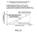
- an ideal frequency of use which is determined from a maximum energization time and a limiting number of store/erase operations as shown in Fig. 21 may be compared with a user's frequency of use, and a notification that the memory has been used to an excessive degree may be provided to the user when the user's frequency of use exceeds the ideal frequency of use.
- the number of erase operations in each block, a maximum number of erase operations, a present energization time, and a maximum energization time are retained in the FeRAM 2, and are outputted to the computer 4 when a self-diagnosis command is accepted.
- the number of write operations are varied depending on blocks, because an amount of writing is increased due to initialization and the like in an early use stage, or the numbers of write operations are not yet completely distributed in an even manner among blocks by wear leveling. For this reason, an alarm is not displayed even if an ideal frequency of use is exceeded when a total of the number of erase operations is small, and an alarm is displayed, for example, when the total of the number of erase operations becomes half or more of the limiting number of store/erase operations.
- an exhaustion level based on a total of the number of erase operations is calculated, but an exhaustion level based on an amount of writing and an amount of reading may be calculated as described in the first embodiment.
- the nonvolatile memory 2 in the memory system of the above described embodiments and background examples may be an MRAM, a PRAM, or an RRAM instead of the FeRAM. Or, it may be composed of a DRAM or SPAM, which is a volatile memory. However, if it is composed of a volatile memory, management information needs to be saved in the NAND type flash memory 1, which is a nonvolatile memory, each time the memory system is powered off.
- a self-diagnosis command may be issued every time the computer 4 is started up.
Landscapes
- Engineering & Computer Science (AREA)
- Theoretical Computer Science (AREA)
- Quality & Reliability (AREA)
- Physics & Mathematics (AREA)
- General Engineering & Computer Science (AREA)
- General Physics & Mathematics (AREA)
- Techniques For Improving Reliability Of Storages (AREA)
- Read Only Memory (AREA)
- For Increasing The Reliability Of Semiconductor Memories (AREA)
- Debugging And Monitoring (AREA)
- Memory System (AREA)
- Iron Core Of Rotating Electric Machines (AREA)
- Soundproofing, Sound Blocking, And Sound Damping (AREA)
- Vehicle Body Suspensions (AREA)
Claims (6)
- Speichersystem, umfassend:einen ersten Speicher (1), in welchen Daten elektrisch geschrieben/gelöscht werden können;einen zweiten Speicher (2), der eingerichtet ist, eine Menge von Schreiben und eine Menge von Lesen hinsichtlich des ersten Speichers (1) zu überwachen und die Menge von Schreiben, die Menge von Lesen und eine begrenzende Menge von Schreiben basierend auf einer Kapazität des ersten Speichers (1) und einer begrenzenden Zahl von Schreib-Operationen zu behalten; undeine Steuerung (3), die verbunden ist, dass ihr ein Selbstdiagnose-Befehl von außen durch eine Verbindungsschnittstelle (31) gegeben wird, und die eingerichtet ist, die Menge von Schreiben, die Menge von Lesen und die begrenzende Menge von Schreiben aus dem zweiten Speicher abzurufen, basierend auf dem Selbstdiagnose-Befehl, und die Menge von Schreiben, die Menge von Lesen und die begrenzende Menge von Schreiben nach außen durch die Verbindungsschnittstelle (31) auszugeben.
- Speichersystem nach Anspruch 1, wobei der zweite Speicher (2) die Zahl von Fehlerbits in einem Speicherblock behält, der eine maximale Zahl von Fehlerbits unter einer Vielzahl von Speicherblöcken aufweist, die in dem ersten Speicher (1) enthalten sind, und die Steuerung (3) eingerichtet ist, die Menge von Schreiben, die Menge von Lesen, die begrenzende Menge von Schreiben und die Zahl von Fehlerbits basierend auf dem Selbstdiagnose-Befehl auszugeben.
- Speichersystem nach Anspruch 1, wobei der zweite Speicher (2) die Zahl von Fehlerbits in wenigstens einem aus der Vielzahl von Speicherblöcken behält, die in dem ersten Speicher (1) enthalten sind und die Steuerung (3) eingerichtet ist, die Menge von Schreiben, die Menge von Lesen, die begrenzende Menge von Schreiben und die Zahl von Fehlerbits basierend auf dem Selbstdiagnose-Befehl auszugeben.
- Speichersystem nach Anspruch 3, wobei der zweite Speicher einen Schwellenwert der Zahl von Fehlerbits behält und die Steuerung eingerichtet ist, die Menge von Schreiben, die Menge von Lesen, die begrenzende Menge von Schreiben, die Zahl von Fehlerbits und den Schwellenwert basierend auf dem Selbstdiagnose-Befehl auszugeben.
- Speichersystem nach Anspruch 1, ferner umfassend einen Zeitzähler (36), der eingerichtet ist, eine Zeit zu messen, die benötigt wird, um Daten in den ersten Speicher (1) zu schreiben,
wobei der zweite Speicher (2) die Menge von Schreiben, die Menge von Lesen, die begrenzende Menge von Schreiben und die Zeit behält, die benötigt wird, um die Daten zu schreiben, und die Steuerung (3) eingerichtet ist, die Menge von Schreiben, die Menge von Lesen, die begrenzende Menge von Schreiben und die Zeit auszugeben, die benötigt wird, um die Daten zu schreiben, basierend auf dem Selbstdiagnose-Befehl. - Speichersystem nach Anspruch 5, wobei der zweite Speicher einen Schwellenwert der Zeit behält, die benötigt wird, um die Daten zu schreiben, und die Steuerung eingerichtet ist, die Menge von Schreiben, die Menge von Lesen, die begrenzende Menge von Schreiben, die Zeit, die benötigt wird, um die Daten zu schreiben, und den Schwellenwert auszugeben, basierend auf dem Selbstdiagnose-Befehl.
Applications Claiming Priority (2)
| Application Number | Priority Date | Filing Date | Title |
|---|---|---|---|
| JP2006322868A JP4575346B2 (ja) | 2006-11-30 | 2006-11-30 | メモリシステム |
| PCT/JP2007/072898 WO2008066058A1 (en) | 2006-11-30 | 2007-11-28 | Memory system |
Publications (3)
| Publication Number | Publication Date |
|---|---|
| EP2088512A1 EP2088512A1 (de) | 2009-08-12 |
| EP2088512A4 EP2088512A4 (de) | 2009-11-25 |
| EP2088512B1 true EP2088512B1 (de) | 2012-02-22 |
Family
ID=39467848
Family Applications (1)
| Application Number | Title | Priority Date | Filing Date |
|---|---|---|---|
| EP07832620A Active EP2088512B1 (de) | 2006-11-30 | 2007-11-28 | Speichersystem |
Country Status (8)
| Country | Link |
|---|---|
| US (3) | USRE47946E1 (de) |
| EP (1) | EP2088512B1 (de) |
| JP (1) | JP4575346B2 (de) |
| KR (1) | KR101079502B1 (de) |
| CN (2) | CN101535967A (de) |
| AT (1) | ATE546782T1 (de) |
| TW (1) | TW200834581A (de) |
| WO (1) | WO2008066058A1 (de) |
Families Citing this family (81)
| Publication number | Priority date | Publication date | Assignee | Title |
|---|---|---|---|---|
| US7653778B2 (en) * | 2006-05-08 | 2010-01-26 | Siliconsystems, Inc. | Systems and methods for measuring the useful life of solid-state storage devices |
| US8549236B2 (en) * | 2006-12-15 | 2013-10-01 | Siliconsystems, Inc. | Storage subsystem with multiple non-volatile memory arrays to protect against data losses |
| KR20090000192A (ko) * | 2007-01-29 | 2009-01-07 | 삼성전자주식회사 | 유효기간 및/ 또는 인듀어런스 데이터를 알려주는 전자시스템 및 그 방법 |
| US7596643B2 (en) * | 2007-02-07 | 2009-09-29 | Siliconsystems, Inc. | Storage subsystem with configurable buffer |
| JP5073402B2 (ja) * | 2007-07-31 | 2012-11-14 | パナソニック株式会社 | メモリーコントローラ、及びこれを用いた不揮発性記憶装置並びに不揮発性記憶システム |
| JP4461170B2 (ja) | 2007-12-28 | 2010-05-12 | 株式会社東芝 | メモリシステム |
| CN101632068B (zh) | 2007-12-28 | 2015-01-14 | 株式会社东芝 | 半导体存储装置 |
| US8078918B2 (en) * | 2008-02-07 | 2011-12-13 | Siliconsystems, Inc. | Solid state storage subsystem that maintains and provides access to data reflective of a failure risk |
| US7962792B2 (en) * | 2008-02-11 | 2011-06-14 | Siliconsystems, Inc. | Interface for enabling a host computer to retrieve device monitor data from a solid state storage subsystem |
| JP4439569B2 (ja) | 2008-04-24 | 2010-03-24 | 株式会社東芝 | メモリシステム |
| JP4683438B2 (ja) * | 2008-06-13 | 2011-05-18 | 讀賣テレビ放送株式会社 | データ放送システム、データ放送方法及びプログラム |
| CN101625901A (zh) * | 2008-07-10 | 2010-01-13 | 深圳市朗科科技股份有限公司 | 半导体存储介质的寿命预警方法、系统及装置 |
| US8140739B2 (en) * | 2008-08-08 | 2012-03-20 | Imation Corp. | Flash memory based storage devices utilizing magnetoresistive random access memory (MRAM) to store files having logical block addresses stored in a write frequency file buffer table |
| JP5319985B2 (ja) * | 2008-08-22 | 2013-10-16 | 株式会社バッファローメモリ | ストレージ機器の使用限界予想方法又はその使用限界予想装置若しくはその使用限界予想時間解析用プログラム |
| JP2010061578A (ja) * | 2008-09-05 | 2010-03-18 | Jds:Kk | 半導体記憶装置の使用限界予想解析用プログラム又はシステム |
| CN101673245B (zh) | 2008-09-09 | 2016-02-03 | 株式会社东芝 | 包括存储器管理装置的信息处理装置和存储器管理方法 |
| JP4575484B2 (ja) | 2008-09-26 | 2010-11-04 | 株式会社東芝 | 記憶装置及び記憶装置の制御方法 |
| US20100125696A1 (en) * | 2008-11-17 | 2010-05-20 | Prasanth Kumar | Memory Controller For Controlling The Wear In A Non-volatile Memory Device And A Method Of Operation Therefor |
| US20100199020A1 (en) * | 2009-02-04 | 2010-08-05 | Silicon Storage Technology, Inc. | Non-volatile memory subsystem and a memory controller therefor |
| JP5268710B2 (ja) * | 2009-02-27 | 2013-08-21 | 株式会社東芝 | 半導体記憶装置 |
| JP4843693B2 (ja) * | 2009-03-30 | 2011-12-21 | 株式会社東芝 | 記憶装置 |
| US8555141B2 (en) * | 2009-06-04 | 2013-10-08 | Lsi Corporation | Flash memory organization |
| US8321639B2 (en) * | 2009-12-30 | 2012-11-27 | Lsi Corporation | Command tracking for direct access block storage devices |
| US8296480B2 (en) * | 2009-11-30 | 2012-10-23 | Lsi Corporation | Context execution in a media controller architecture |
| US8516264B2 (en) * | 2009-10-09 | 2013-08-20 | Lsi Corporation | Interlocking plain text passwords to data encryption keys |
| US8219776B2 (en) * | 2009-09-23 | 2012-07-10 | Lsi Corporation | Logical-to-physical address translation for solid state disks |
| US7975193B2 (en) * | 2009-06-01 | 2011-07-05 | Lsi Corporation | Solid state storage end of life prediction with correction history |
| US8245112B2 (en) * | 2009-06-04 | 2012-08-14 | Lsi Corporation | Flash memory organization |
| US20100306451A1 (en) * | 2009-06-01 | 2010-12-02 | Joshua Johnson | Architecture for nand flash constraint enforcement |
| US8166258B2 (en) * | 2009-07-24 | 2012-04-24 | Lsi Corporation | Skip operations for solid state disks |
| JP2011186553A (ja) * | 2010-03-04 | 2011-09-22 | Toshiba Corp | メモリ管理装置 |
| JP2011070346A (ja) * | 2009-09-25 | 2011-04-07 | Toshiba Corp | メモリシステム |
| CN102597906B (zh) * | 2009-11-06 | 2016-02-03 | 飞思卡尔半导体公司 | 对电子器件中的损耗的响应 |
| JP4762342B2 (ja) * | 2009-12-25 | 2011-08-31 | 株式会社東芝 | 記録制御装置及び記録制御方法 |
| JP2011164994A (ja) | 2010-02-10 | 2011-08-25 | Toshiba Corp | メモリシステム |
| US9170933B2 (en) | 2010-06-28 | 2015-10-27 | International Business Machines Corporation | Wear-level of cells/pages/sub-pages/blocks of a memory |
| JP2012079100A (ja) * | 2010-10-01 | 2012-04-19 | Canon Inc | ディスク制御装置及びディスク制御方法、並びにプログラム |
| KR101190742B1 (ko) * | 2010-12-06 | 2012-10-12 | 에스케이하이닉스 주식회사 | 메모리의 콘트롤러 및 이를 포함하는 스토리지 시스템, 메모리의 수명 측정 방법 |
| EP2659489A1 (de) * | 2011-04-28 | 2013-11-06 | Hitachi, Ltd. | Halbleiterspeichervorrichtung und verfahren zur steuerung der halbleiterspeichervorrichtung |
| CN102163165B (zh) * | 2011-05-26 | 2012-11-14 | 忆正存储技术(武汉)有限公司 | 一种闪存错误预估模块及其预估方法 |
| US8719531B2 (en) | 2011-06-14 | 2014-05-06 | Western Digital Technologies, Inc. | System and method for performing data retention that incorporates environmental conditions |
| EP2745203B1 (de) | 2011-08-19 | 2016-09-21 | Kabushiki Kaisha Toshiba | Informationsverarbeitungsvorrichtung |
| CN102956266B (zh) * | 2011-08-30 | 2015-08-05 | 株式会社理光 | 一种在图像形成装置的引擎部中使用的信息存储方法 |
| CN102999448B (zh) * | 2011-09-14 | 2018-07-06 | 奇智软件(北京)有限公司 | 一种外部设备检测的处理方法及装置 |
| JP5222388B2 (ja) * | 2011-11-22 | 2013-06-26 | 株式会社日立製作所 | フラッシュメモリを用いたストレージシステムの管理システム及び管理方法 |
| TWI455140B (zh) * | 2012-02-21 | 2014-10-01 | Fluiditech Ip Ltd | Flash memory usage period assessment method |
| US20130262942A1 (en) * | 2012-03-27 | 2013-10-03 | Yung-Chiang Chu | Flash memory lifetime evaluation method |
| US20140013028A1 (en) * | 2012-07-09 | 2014-01-09 | Hamilton Sundstrand Corporation | Hardware flash memory wear monitoring |
| US20140095778A1 (en) * | 2012-09-28 | 2014-04-03 | Jaewoong Chung | Methods, systems and apparatus to cache code in non-volatile memory |
| GB2514354A (en) * | 2013-05-20 | 2014-11-26 | Ibm | Managing storage devices having a lifetime of a finite number of operations |
| US9875810B2 (en) * | 2013-07-24 | 2018-01-23 | Microsoft Technology Licensing, Llc | Self-identifying memory errors |
| CN103559115A (zh) * | 2013-09-29 | 2014-02-05 | 记忆科技(深圳)有限公司 | 基于smart的ssd智能监控系统 |
| US9612773B2 (en) * | 2013-11-21 | 2017-04-04 | Samsung Electronics Co., Ltd. | User device having a host flash translation layer (FTL), a method for transferring an erase count thereof, a method for transferring reprogram information thereof, and a method for transferring a page offset of an open block thereof |
| CN103678150B (zh) * | 2013-12-23 | 2017-06-09 | 华为技术有限公司 | 固态硬盘使用方法及装置 |
| CN105005450B (zh) * | 2014-04-25 | 2018-11-02 | 群联电子股份有限公司 | 数据写入方法、存储器存储装置及存储器控制电路单元 |
| KR101628925B1 (ko) * | 2014-06-17 | 2016-06-10 | 고려대학교 산학협력단 | 메모리 시스템 및 메모리 시스템의 동작 방법 |
| CN105512056A (zh) * | 2014-09-24 | 2016-04-20 | 中兴通讯股份有限公司 | 数据保存方法、装置及终端 |
| JP6421042B2 (ja) * | 2015-01-16 | 2018-11-07 | ルネサスエレクトロニクス株式会社 | 情報処理装置 |
| JP6365341B2 (ja) * | 2015-02-23 | 2018-08-01 | 京セラドキュメントソリューションズ株式会社 | 画像形成装置 |
| JP6541369B2 (ja) * | 2015-02-24 | 2019-07-10 | キヤノン株式会社 | メモリのデータ処理を行なうデータ処理装置、データ処理方法、及びプログラム |
| CN105373350A (zh) * | 2015-11-23 | 2016-03-02 | 联想(北京)有限公司 | 一种数据管理方法及装置 |
| CN106779008A (zh) * | 2015-11-23 | 2017-05-31 | 杭州海康威视数字技术股份有限公司 | Sd卡、摄像机和sd卡可靠性预警系统 |
| JP6515799B2 (ja) * | 2015-12-18 | 2019-05-22 | 京セラドキュメントソリューションズ株式会社 | 電子機器及びメモリー寿命警告プログラム |
| JP6432499B2 (ja) * | 2015-12-18 | 2018-12-05 | 京セラドキュメントソリューションズ株式会社 | 電子機器及びメモリー寿命警告プログラム |
| US10558369B2 (en) * | 2016-02-01 | 2020-02-11 | Qualcomm Incorporated | Flash device lifetime monitor systems and methods |
| JP6190488B2 (ja) * | 2016-04-15 | 2017-08-30 | 東芝メモリ株式会社 | 情報記録システム |
| US10514867B2 (en) | 2016-11-10 | 2019-12-24 | Western Digital Technologies, Inc. | System and methodology that facilitates error management within a shared non-volatile memory architecture |
| US10254982B2 (en) * | 2016-11-10 | 2019-04-09 | Western Digital Technologies, Inc. | System and methodology for low latency error management within a shared non-volatile memory architecture |
| JP2018156582A (ja) * | 2017-03-21 | 2018-10-04 | キヤノン株式会社 | 情報処理装置および画像形成装置等のストレージ制御方法 |
| CN106980566B (zh) * | 2017-03-27 | 2020-05-26 | 联想(北京)有限公司 | 一种显示控制方法及存储装置 |
| JP7010667B2 (ja) | 2017-11-06 | 2022-01-26 | キオクシア株式会社 | メモリシステムおよび制御方法 |
| US10714187B2 (en) | 2018-01-11 | 2020-07-14 | Raymx Microelectronics Corp. | Memory control device for estimating time interval and method thereof |
| TWI692691B (zh) | 2018-01-11 | 2020-05-01 | 大陸商合肥沛睿微電子股份有限公司 | 記憶體控制裝置與記憶體控制方法 |
| JP6913797B2 (ja) * | 2018-08-31 | 2021-08-04 | キオクシア株式会社 | 情報処理装置 |
| KR102599176B1 (ko) * | 2018-11-14 | 2023-11-08 | 삼성전자주식회사 | 호스트 메모리 버퍼를 사용하는 스토리지 장치 및 그것의 메모리 관리 방법 |
| WO2020161981A1 (ja) * | 2019-02-06 | 2020-08-13 | ソニー株式会社 | メモリ診断装置およびメモリ診断方法 |
| JP7143487B2 (ja) * | 2020-05-18 | 2022-09-28 | キオクシア株式会社 | 情報処理装置 |
| JP7097631B2 (ja) * | 2020-11-04 | 2022-07-08 | 株式会社ユピテル | システム及びプログラム |
| KR102775528B1 (ko) | 2021-03-02 | 2025-03-07 | 삼성전자주식회사 | 쓰기 동작을 리디렉션하는 스토리지 컨트롤러 및 이의 동작 방법 |
| CN114420183A (zh) * | 2022-01-24 | 2022-04-29 | 珠海奔图电子有限公司 | 数据存储控制方法、电子设备及存储介质 |
| CN115132266A (zh) * | 2022-06-29 | 2022-09-30 | 深圳市德明利技术股份有限公司 | 数据保护方法、装置、终端设备及可读存储介质 |
Family Cites Families (21)
| Publication number | Priority date | Publication date | Assignee | Title |
|---|---|---|---|---|
| US265545A (en) * | 1882-10-03 | Emanuel m | ||
| US4224506A (en) * | 1978-03-24 | 1980-09-23 | Pitney Bowes Inc. | Electronic counter with non-volatile memory |
| US6078520A (en) * | 1993-04-08 | 2000-06-20 | Hitachi, Ltd. | Flash memory control method and information processing system therewith |
| JP3242890B2 (ja) * | 1998-12-16 | 2001-12-25 | 株式会社ハギワラシスコム | 記憶装置 |
| US6249838B1 (en) * | 1998-12-28 | 2001-06-19 | Cisco Technology Inc. | Physical medium information in file system header |
| JP2001195316A (ja) * | 2000-01-14 | 2001-07-19 | Canon Inc | バックアップ記憶装置、画像形成装置、バックアップ記憶装置制御方法及び記憶媒体 |
| US20020091965A1 (en) * | 2000-12-22 | 2002-07-11 | Mark Moshayedi | System and method for early detection of impending failure of a data storage system |
| US6426898B1 (en) * | 2001-03-05 | 2002-07-30 | Micron Technology, Inc. | Method of reducing trapped holes induced by erase operations in the tunnel oxide of flash memory cells |
| US6775624B2 (en) * | 2001-10-19 | 2004-08-10 | International Business Machines Corporation | Method and apparatus for estimating remaining life of a product |
| JP2003216506A (ja) * | 2002-01-23 | 2003-07-31 | Hitachi Ltd | フラッシュメモリを搭載した記憶装置及び計算機 |
| US6751766B2 (en) * | 2002-05-20 | 2004-06-15 | Sandisk Corporation | Increasing the effectiveness of error correction codes and operating multi-level memory systems by using information about the quality of the stored data |
| JP4381740B2 (ja) * | 2002-08-15 | 2009-12-09 | 独立行政法人産業技術総合研究所 | 光記録再生装置、光記録再生方法及び光記録媒体 |
| JP4110000B2 (ja) * | 2003-01-28 | 2008-07-02 | 株式会社ルネサステクノロジ | 記憶装置 |
| JP4073799B2 (ja) | 2003-02-07 | 2008-04-09 | 株式会社ルネサステクノロジ | メモリシステム |
| DE102004034042A1 (de) * | 2004-07-13 | 2006-02-09 | Endress + Hauser Gmbh + Co. Kg | Elektronisches Gerät mit einem nicht flüchtigen beschreibbaren Datenspeicher |
| JP4215746B2 (ja) * | 2005-05-20 | 2009-01-28 | Necインフロンティア株式会社 | 情報処理装置および寿命監視方法 |
| US7512847B2 (en) * | 2006-02-10 | 2009-03-31 | Sandisk Il Ltd. | Method for estimating and reporting the life expectancy of flash-disk memory |
| CN1858855A (zh) | 2006-02-17 | 2006-11-08 | 华为技术有限公司 | 一种延长非易失存储器寿命的计数方法和装置 |
| US7653778B2 (en) * | 2006-05-08 | 2010-01-26 | Siliconsystems, Inc. | Systems and methods for measuring the useful life of solid-state storage devices |
| US7523013B2 (en) * | 2006-05-15 | 2009-04-21 | Sandisk Corporation | Methods of end of life calculation for non-volatile memories |
| US7356442B1 (en) * | 2006-10-05 | 2008-04-08 | International Business Machines Corporation | End of life prediction of flash memory |
-
2006
- 2006-11-30 JP JP2006322868A patent/JP4575346B2/ja active Active
-
2007
- 2007-11-28 CN CNA2007800425527A patent/CN101535967A/zh active Pending
- 2007-11-28 US US14/249,070 patent/USRE47946E1/en active Active
- 2007-11-28 KR KR1020097011144A patent/KR101079502B1/ko active Active
- 2007-11-28 CN CN201510111605.2A patent/CN104699546A/zh active Pending
- 2007-11-28 US US12/513,860 patent/US8156393B2/en not_active Ceased
- 2007-11-28 AT AT07832620T patent/ATE546782T1/de active
- 2007-11-28 EP EP07832620A patent/EP2088512B1/de active Active
- 2007-11-28 WO PCT/JP2007/072898 patent/WO2008066058A1/ja not_active Ceased
- 2007-11-30 TW TW096145749A patent/TW200834581A/zh unknown
-
2012
- 2012-03-22 US US13/426,696 patent/US20120179942A1/en not_active Abandoned
Also Published As
| Publication number | Publication date |
|---|---|
| US20100011260A1 (en) | 2010-01-14 |
| KR101079502B1 (ko) | 2011-11-03 |
| CN104699546A (zh) | 2015-06-10 |
| US20120179942A1 (en) | 2012-07-12 |
| CN101535967A (zh) | 2009-09-16 |
| KR20090079969A (ko) | 2009-07-22 |
| WO2008066058A1 (en) | 2008-06-05 |
| TW200834581A (en) | 2008-08-16 |
| TWI380302B (de) | 2012-12-21 |
| EP2088512A4 (de) | 2009-11-25 |
| US8156393B2 (en) | 2012-04-10 |
| ATE546782T1 (de) | 2012-03-15 |
| JP4575346B2 (ja) | 2010-11-04 |
| JP2008139927A (ja) | 2008-06-19 |
| EP2088512A1 (de) | 2009-08-12 |
| USRE47946E1 (en) | 2020-04-14 |
Similar Documents
| Publication | Publication Date | Title |
|---|---|---|
| EP2088512B1 (de) | Speichersystem | |
| US10020072B2 (en) | Detect developed bad blocks in non-volatile memory devices | |
| TWI431476B (zh) | 操作一記憶體系統、一包含一主機與一記憶體系統之系統、及一或多個記憶體裝置與一主機之方法 | |
| US7962807B2 (en) | Semiconductor storage apparatus managing system, semiconductor storage apparatus, host apparatus, program and method of managing semiconductor storage apparatus | |
| US20200167083A1 (en) | Techniques for controlling recycling of blocks of memory | |
| US10657014B2 (en) | Methods for monitoring and managing memory devices | |
| KR101608679B1 (ko) | 톤 라이트 완화 | |
| US10592134B1 (en) | Open block stability scanning | |
| US9263158B2 (en) | Determining data retention time in a solid-state non-volatile memory | |
| US20100061207A1 (en) | Data storage device including self-test features | |
| CN103136118A (zh) | 使用多层存储器的磁盘驱动数据缓存 | |
| JP2009512119A (ja) | 訂正済みデータの格納および処理方法 | |
| CN114661237B (zh) | 一种存储管理方法、装置、程序及设备 | |
| US11513890B1 (en) | Adaptive read scrub | |
| US7904637B2 (en) | Information processing apparatus, lifetime monitoring method and program for monitoring lifetime of storage device including flash memory | |
| CN108564981B (zh) | 一种存储装置数据安全动态监控方法 | |
| JP2012234321A (ja) | 記録再生装置 | |
| CN116868270A (zh) | 用于改进存储器的ecc操作的方法及系统 | |
| US7962810B2 (en) | Recording medium structure capable of displaying defect rate | |
| US10475522B2 (en) | Memory system including a delegate page and method of identifying a status of a memory system | |
| JP5678628B2 (ja) | 半導体ディスク装置 | |
| JP2010192047A (ja) | ディスクドライブ装置及び不揮発性メモリ制御方法 | |
| Janukowicz et al. | IN THIS WHITE PAPER |
Legal Events
| Date | Code | Title | Description |
|---|---|---|---|
| PUAI | Public reference made under article 153(3) epc to a published international application that has entered the european phase |
Free format text: ORIGINAL CODE: 0009012 |
|
| 17P | Request for examination filed |
Effective date: 20090428 |
|
| AK | Designated contracting states |
Kind code of ref document: A1 Designated state(s): AT BE BG CH CY CZ DE DK EE ES FI FR GB GR HU IE IS IT LI LT LU LV MC MT NL PL PT RO SE SI SK TR |
|
| A4 | Supplementary search report drawn up and despatched |
Effective date: 20091028 |
|
| 17Q | First examination report despatched |
Effective date: 20100210 |
|
| DAX | Request for extension of the european patent (deleted) | ||
| GRAP | Despatch of communication of intention to grant a patent |
Free format text: ORIGINAL CODE: EPIDOSNIGR1 |
|
| GRAS | Grant fee paid |
Free format text: ORIGINAL CODE: EPIDOSNIGR3 |
|
| GRAA | (expected) grant |
Free format text: ORIGINAL CODE: 0009210 |
|
| AK | Designated contracting states |
Kind code of ref document: B1 Designated state(s): AT BE BG CH CY CZ DE DK EE ES FI FR GB GR HU IE IS IT LI LT LU LV MC MT NL PL PT RO SE SI SK TR |
|
| REG | Reference to a national code |
Ref country code: GB Ref legal event code: FG4D |
|
| REG | Reference to a national code |
Ref country code: CH Ref legal event code: EP |
|
| REG | Reference to a national code |
Ref country code: AT Ref legal event code: REF Ref document number: 546782 Country of ref document: AT Kind code of ref document: T Effective date: 20120315 |
|
| REG | Reference to a national code |
Ref country code: IE Ref legal event code: FG4D |
|
| REG | Reference to a national code |
Ref country code: DE Ref legal event code: R096 Ref document number: 602007020906 Country of ref document: DE Effective date: 20120419 |
|
| REG | Reference to a national code |
Ref country code: NL Ref legal event code: VDEP Effective date: 20120222 |
|
| LTIE | Lt: invalidation of european patent or patent extension |
Effective date: 20120222 |
|
| PG25 | Lapsed in a contracting state [announced via postgrant information from national office to epo] |
Ref country code: IS Free format text: LAPSE BECAUSE OF FAILURE TO SUBMIT A TRANSLATION OF THE DESCRIPTION OR TO PAY THE FEE WITHIN THE PRESCRIBED TIME-LIMIT Effective date: 20120622 Ref country code: NL Free format text: LAPSE BECAUSE OF FAILURE TO SUBMIT A TRANSLATION OF THE DESCRIPTION OR TO PAY THE FEE WITHIN THE PRESCRIBED TIME-LIMIT Effective date: 20120222 Ref country code: LT Free format text: LAPSE BECAUSE OF FAILURE TO SUBMIT A TRANSLATION OF THE DESCRIPTION OR TO PAY THE FEE WITHIN THE PRESCRIBED TIME-LIMIT Effective date: 20120222 |
|
| PG25 | Lapsed in a contracting state [announced via postgrant information from national office to epo] |
Ref country code: FI Free format text: LAPSE BECAUSE OF FAILURE TO SUBMIT A TRANSLATION OF THE DESCRIPTION OR TO PAY THE FEE WITHIN THE PRESCRIBED TIME-LIMIT Effective date: 20120222 Ref country code: BE Free format text: LAPSE BECAUSE OF FAILURE TO SUBMIT A TRANSLATION OF THE DESCRIPTION OR TO PAY THE FEE WITHIN THE PRESCRIBED TIME-LIMIT Effective date: 20120222 Ref country code: PT Free format text: LAPSE BECAUSE OF FAILURE TO SUBMIT A TRANSLATION OF THE DESCRIPTION OR TO PAY THE FEE WITHIN THE PRESCRIBED TIME-LIMIT Effective date: 20120622 Ref country code: LV Free format text: LAPSE BECAUSE OF FAILURE TO SUBMIT A TRANSLATION OF THE DESCRIPTION OR TO PAY THE FEE WITHIN THE PRESCRIBED TIME-LIMIT Effective date: 20120222 Ref country code: GR Free format text: LAPSE BECAUSE OF FAILURE TO SUBMIT A TRANSLATION OF THE DESCRIPTION OR TO PAY THE FEE WITHIN THE PRESCRIBED TIME-LIMIT Effective date: 20120523 |
|
| REG | Reference to a national code |
Ref country code: AT Ref legal event code: MK05 Ref document number: 546782 Country of ref document: AT Kind code of ref document: T Effective date: 20120222 |
|
| PG25 | Lapsed in a contracting state [announced via postgrant information from national office to epo] |
Ref country code: CY Free format text: LAPSE BECAUSE OF FAILURE TO SUBMIT A TRANSLATION OF THE DESCRIPTION OR TO PAY THE FEE WITHIN THE PRESCRIBED TIME-LIMIT Effective date: 20120222 |
|
| PG25 | Lapsed in a contracting state [announced via postgrant information from national office to epo] |
Ref country code: SE Free format text: LAPSE BECAUSE OF FAILURE TO SUBMIT A TRANSLATION OF THE DESCRIPTION OR TO PAY THE FEE WITHIN THE PRESCRIBED TIME-LIMIT Effective date: 20120222 Ref country code: CZ Free format text: LAPSE BECAUSE OF FAILURE TO SUBMIT A TRANSLATION OF THE DESCRIPTION OR TO PAY THE FEE WITHIN THE PRESCRIBED TIME-LIMIT Effective date: 20120222 Ref country code: RO Free format text: LAPSE BECAUSE OF FAILURE TO SUBMIT A TRANSLATION OF THE DESCRIPTION OR TO PAY THE FEE WITHIN THE PRESCRIBED TIME-LIMIT Effective date: 20120222 Ref country code: PL Free format text: LAPSE BECAUSE OF FAILURE TO SUBMIT A TRANSLATION OF THE DESCRIPTION OR TO PAY THE FEE WITHIN THE PRESCRIBED TIME-LIMIT Effective date: 20120222 Ref country code: DK Free format text: LAPSE BECAUSE OF FAILURE TO SUBMIT A TRANSLATION OF THE DESCRIPTION OR TO PAY THE FEE WITHIN THE PRESCRIBED TIME-LIMIT Effective date: 20120222 Ref country code: EE Free format text: LAPSE BECAUSE OF FAILURE TO SUBMIT A TRANSLATION OF THE DESCRIPTION OR TO PAY THE FEE WITHIN THE PRESCRIBED TIME-LIMIT Effective date: 20120222 Ref country code: SI Free format text: LAPSE BECAUSE OF FAILURE TO SUBMIT A TRANSLATION OF THE DESCRIPTION OR TO PAY THE FEE WITHIN THE PRESCRIBED TIME-LIMIT Effective date: 20120222 |
|
| PG25 | Lapsed in a contracting state [announced via postgrant information from national office to epo] |
Ref country code: IT Free format text: LAPSE BECAUSE OF FAILURE TO SUBMIT A TRANSLATION OF THE DESCRIPTION OR TO PAY THE FEE WITHIN THE PRESCRIBED TIME-LIMIT Effective date: 20120222 Ref country code: SK Free format text: LAPSE BECAUSE OF FAILURE TO SUBMIT A TRANSLATION OF THE DESCRIPTION OR TO PAY THE FEE WITHIN THE PRESCRIBED TIME-LIMIT Effective date: 20120222 |
|
| PLBE | No opposition filed within time limit |
Free format text: ORIGINAL CODE: 0009261 |
|
| STAA | Information on the status of an ep patent application or granted ep patent |
Free format text: STATUS: NO OPPOSITION FILED WITHIN TIME LIMIT |
|
| 26N | No opposition filed |
Effective date: 20121123 |
|
| PG25 | Lapsed in a contracting state [announced via postgrant information from national office to epo] |
Ref country code: AT Free format text: LAPSE BECAUSE OF FAILURE TO SUBMIT A TRANSLATION OF THE DESCRIPTION OR TO PAY THE FEE WITHIN THE PRESCRIBED TIME-LIMIT Effective date: 20120222 |
|
| REG | Reference to a national code |
Ref country code: DE Ref legal event code: R097 Ref document number: 602007020906 Country of ref document: DE Effective date: 20121123 |
|
| PG25 | Lapsed in a contracting state [announced via postgrant information from national office to epo] |
Ref country code: ES Free format text: LAPSE BECAUSE OF FAILURE TO SUBMIT A TRANSLATION OF THE DESCRIPTION OR TO PAY THE FEE WITHIN THE PRESCRIBED TIME-LIMIT Effective date: 20120602 |
|
| REG | Reference to a national code |
Ref country code: CH Ref legal event code: PL |
|
| PG25 | Lapsed in a contracting state [announced via postgrant information from national office to epo] |
Ref country code: LI Free format text: LAPSE BECAUSE OF NON-PAYMENT OF DUE FEES Effective date: 20121130 Ref country code: CH Free format text: LAPSE BECAUSE OF NON-PAYMENT OF DUE FEES Effective date: 20121130 Ref country code: BG Free format text: LAPSE BECAUSE OF FAILURE TO SUBMIT A TRANSLATION OF THE DESCRIPTION OR TO PAY THE FEE WITHIN THE PRESCRIBED TIME-LIMIT Effective date: 20120522 |
|
| REG | Reference to a national code |
Ref country code: IE Ref legal event code: MM4A |
|
| PG25 | Lapsed in a contracting state [announced via postgrant information from national office to epo] |
Ref country code: IE Free format text: LAPSE BECAUSE OF NON-PAYMENT OF DUE FEES Effective date: 20121128 |
|
| PG25 | Lapsed in a contracting state [announced via postgrant information from national office to epo] |
Ref country code: MT Free format text: LAPSE BECAUSE OF FAILURE TO SUBMIT A TRANSLATION OF THE DESCRIPTION OR TO PAY THE FEE WITHIN THE PRESCRIBED TIME-LIMIT Effective date: 20120222 |
|
| PG25 | Lapsed in a contracting state [announced via postgrant information from national office to epo] |
Ref country code: MC Free format text: LAPSE BECAUSE OF NON-PAYMENT OF DUE FEES Effective date: 20121130 Ref country code: TR Free format text: LAPSE BECAUSE OF FAILURE TO SUBMIT A TRANSLATION OF THE DESCRIPTION OR TO PAY THE FEE WITHIN THE PRESCRIBED TIME-LIMIT Effective date: 20120222 |
|
| PG25 | Lapsed in a contracting state [announced via postgrant information from national office to epo] |
Ref country code: LU Free format text: LAPSE BECAUSE OF NON-PAYMENT OF DUE FEES Effective date: 20121128 |
|
| PG25 | Lapsed in a contracting state [announced via postgrant information from national office to epo] |
Ref country code: HU Free format text: LAPSE BECAUSE OF FAILURE TO SUBMIT A TRANSLATION OF THE DESCRIPTION OR TO PAY THE FEE WITHIN THE PRESCRIBED TIME-LIMIT Effective date: 20071128 |
|
| REG | Reference to a national code |
Ref country code: FR Ref legal event code: PLFP Year of fee payment: 9 |
|
| REG | Reference to a national code |
Ref country code: FR Ref legal event code: PLFP Year of fee payment: 10 |
|
| REG | Reference to a national code |
Ref country code: DE Ref legal event code: R081 Ref document number: 602007020906 Country of ref document: DE Owner name: KIOXIA CORPORATION, JP Free format text: FORMER OWNER: KABUSHIKI KAISHA TOSHIBA, MINATO-KU, TOKYO, JP Ref country code: DE Ref legal event code: R082 Ref document number: 602007020906 Country of ref document: DE Representative=s name: HOFFMANN - EITLE PATENT- UND RECHTSANWAELTE PA, DE Ref country code: DE Ref legal event code: R081 Ref document number: 602007020906 Country of ref document: DE Owner name: TOSHIBA MEMORY CORPORATION, JP Free format text: FORMER OWNER: KABUSHIKI KAISHA TOSHIBA, MINATO-KU, TOKYO, JP |
|
| REG | Reference to a national code |
Ref country code: GB Ref legal event code: 732E Free format text: REGISTERED BETWEEN 20170914 AND 20170920 |
|
| REG | Reference to a national code |
Ref country code: FR Ref legal event code: PLFP Year of fee payment: 11 |
|
| REG | Reference to a national code |
Ref country code: FR Ref legal event code: TP Owner name: TOSHIBA MEMORY CORPORATION, JP Effective date: 20171205 |
|
| REG | Reference to a national code |
Ref country code: FR Ref legal event code: PLFP Year of fee payment: 12 |
|
| REG | Reference to a national code |
Ref country code: DE Ref legal event code: R081 Ref document number: 602007020906 Country of ref document: DE Owner name: KIOXIA CORPORATION, JP Free format text: FORMER OWNER: TOSHIBA MEMORY CORPORATION, TOKYO, JP |
|
| REG | Reference to a national code |
Ref country code: GB Ref legal event code: 732E Free format text: REGISTERED BETWEEN 20220127 AND 20220202 |
|
| PGFP | Annual fee paid to national office [announced via postgrant information from national office to epo] |
Ref country code: DE Payment date: 20251119 Year of fee payment: 19 |
|
| PGFP | Annual fee paid to national office [announced via postgrant information from national office to epo] |
Ref country code: GB Payment date: 20251121 Year of fee payment: 19 |
|
| PGFP | Annual fee paid to national office [announced via postgrant information from national office to epo] |
Ref country code: FR Payment date: 20251121 Year of fee payment: 19 |