EP2088620B1 - Dispositif semiconducteur - Google Patents
Dispositif semiconducteur Download PDFInfo
- Publication number
- EP2088620B1 EP2088620B1 EP07830374.0A EP07830374A EP2088620B1 EP 2088620 B1 EP2088620 B1 EP 2088620B1 EP 07830374 A EP07830374 A EP 07830374A EP 2088620 B1 EP2088620 B1 EP 2088620B1
- Authority
- EP
- European Patent Office
- Prior art keywords
- source
- drain
- pad
- substrate
- electrode wiring
- Prior art date
- Legal status (The legal status is an assumption and is not a legal conclusion. Google has not performed a legal analysis and makes no representation as to the accuracy of the status listed.)
- Not-in-force
Links
Images


Classifications
-
- H—ELECTRICITY
- H10—SEMICONDUCTOR DEVICES; ELECTRIC SOLID-STATE DEVICES NOT OTHERWISE PROVIDED FOR
- H10W—GENERIC PACKAGES, INTERCONNECTIONS, CONNECTORS OR OTHER CONSTRUCTIONAL DETAILS OF DEVICES COVERED BY CLASS H10
- H10W20/00—Interconnections in chips, wafers or substrates
- H10W20/40—Interconnections external to wafers or substrates, e.g. back-end-of-line [BEOL] metallisations or vias connecting to gate electrodes
- H10W20/482—Interconnections external to wafers or substrates, e.g. back-end-of-line [BEOL] metallisations or vias connecting to gate electrodes for individual devices provided for in groups H10D8/00 - H10D48/00, e.g. for power transistors
- H10W20/484—Interconnections having extended contours, e.g. pads having mesh shape or interconnections comprising connected parallel stripes
-
- H—ELECTRICITY
- H10—SEMICONDUCTOR DEVICES; ELECTRIC SOLID-STATE DEVICES NOT OTHERWISE PROVIDED FOR
- H10D—INORGANIC ELECTRIC SEMICONDUCTOR DEVICES
- H10D30/00—Field-effect transistors [FET]
- H10D30/80—FETs having rectifying junction gate electrodes
- H10D30/87—FETs having Schottky gate electrodes, e.g. metal-semiconductor FETs [MESFET]
-
- H—ELECTRICITY
- H10—SEMICONDUCTOR DEVICES; ELECTRIC SOLID-STATE DEVICES NOT OTHERWISE PROVIDED FOR
- H10P—GENERIC PROCESSES OR APPARATUS FOR THE MANUFACTURE OR TREATMENT OF DEVICES COVERED BY CLASS H10
- H10P10/00—Bonding of wafers, substrates or parts of devices
-
- H—ELECTRICITY
- H10—SEMICONDUCTOR DEVICES; ELECTRIC SOLID-STATE DEVICES NOT OTHERWISE PROVIDED FOR
- H10W—GENERIC PACKAGES, INTERCONNECTIONS, CONNECTORS OR OTHER CONSTRUCTIONAL DETAILS OF DEVICES COVERED BY CLASS H10
- H10W44/00—Electrical arrangements for controlling or matching impedance
- H10W44/20—Electrical arrangements for controlling or matching impedance at high-frequency [HF] or radio frequency [RF]
-
- H—ELECTRICITY
- H10—SEMICONDUCTOR DEVICES; ELECTRIC SOLID-STATE DEVICES NOT OTHERWISE PROVIDED FOR
- H10W—GENERIC PACKAGES, INTERCONNECTIONS, CONNECTORS OR OTHER CONSTRUCTIONAL DETAILS OF DEVICES COVERED BY CLASS H10
- H10W72/00—Interconnections or connectors in packages
- H10W72/90—Bond pads, in general
-
- H—ELECTRICITY
- H10—SEMICONDUCTOR DEVICES; ELECTRIC SOLID-STATE DEVICES NOT OTHERWISE PROVIDED FOR
- H10W—GENERIC PACKAGES, INTERCONNECTIONS, CONNECTORS OR OTHER CONSTRUCTIONAL DETAILS OF DEVICES COVERED BY CLASS H10
- H10W20/00—Interconnections in chips, wafers or substrates
- H10W20/40—Interconnections external to wafers or substrates, e.g. back-end-of-line [BEOL] metallisations or vias connecting to gate electrodes
- H10W20/482—Interconnections external to wafers or substrates, e.g. back-end-of-line [BEOL] metallisations or vias connecting to gate electrodes for individual devices provided for in groups H10D8/00 - H10D48/00, e.g. for power transistors
- H10W20/483—Interconnections over air gaps, e.g. air bridges
-
- H—ELECTRICITY
- H10—SEMICONDUCTOR DEVICES; ELECTRIC SOLID-STATE DEVICES NOT OTHERWISE PROVIDED FOR
- H10W—GENERIC PACKAGES, INTERCONNECTIONS, CONNECTORS OR OTHER CONSTRUCTIONAL DETAILS OF DEVICES COVERED BY CLASS H10
- H10W44/00—Electrical arrangements for controlling or matching impedance
- H10W44/20—Electrical arrangements for controlling or matching impedance at high-frequency [HF] or radio frequency [RF]
- H10W44/203—Electrical connections
- H10W44/206—Wires
-
- H—ELECTRICITY
- H10—SEMICONDUCTOR DEVICES; ELECTRIC SOLID-STATE DEVICES NOT OTHERWISE PROVIDED FOR
- H10W—GENERIC PACKAGES, INTERCONNECTIONS, CONNECTORS OR OTHER CONSTRUCTIONAL DETAILS OF DEVICES COVERED BY CLASS H10
- H10W44/00—Electrical arrangements for controlling or matching impedance
- H10W44/20—Electrical arrangements for controlling or matching impedance at high-frequency [HF] or radio frequency [RF]
- H10W44/226—Electrical arrangements for controlling or matching impedance at high-frequency [HF] or radio frequency [RF] for HF amplifiers
-
- H—ELECTRICITY
- H10—SEMICONDUCTOR DEVICES; ELECTRIC SOLID-STATE DEVICES NOT OTHERWISE PROVIDED FOR
- H10W—GENERIC PACKAGES, INTERCONNECTIONS, CONNECTORS OR OTHER CONSTRUCTIONAL DETAILS OF DEVICES COVERED BY CLASS H10
- H10W70/00—Package substrates; Interposers; Redistribution layers [RDL]
- H10W70/60—Insulating or insulated package substrates; Interposers; Redistribution layers
-
- H—ELECTRICITY
- H10—SEMICONDUCTOR DEVICES; ELECTRIC SOLID-STATE DEVICES NOT OTHERWISE PROVIDED FOR
- H10W—GENERIC PACKAGES, INTERCONNECTIONS, CONNECTORS OR OTHER CONSTRUCTIONAL DETAILS OF DEVICES COVERED BY CLASS H10
- H10W72/00—Interconnections or connectors in packages
- H10W72/071—Connecting or disconnecting
- H10W72/075—Connecting or disconnecting of bond wires
- H10W72/07541—Controlling the environment, e.g. atmosphere composition or temperature
- H10W72/07552—Controlling the environment, e.g. atmosphere composition or temperature changes in structures or sizes
-
- H—ELECTRICITY
- H10—SEMICONDUCTOR DEVICES; ELECTRIC SOLID-STATE DEVICES NOT OTHERWISE PROVIDED FOR
- H10W—GENERIC PACKAGES, INTERCONNECTIONS, CONNECTORS OR OTHER CONSTRUCTIONAL DETAILS OF DEVICES COVERED BY CLASS H10
- H10W72/00—Interconnections or connectors in packages
- H10W72/50—Bond wires
-
- H—ELECTRICITY
- H10—SEMICONDUCTOR DEVICES; ELECTRIC SOLID-STATE DEVICES NOT OTHERWISE PROVIDED FOR
- H10W—GENERIC PACKAGES, INTERCONNECTIONS, CONNECTORS OR OTHER CONSTRUCTIONAL DETAILS OF DEVICES COVERED BY CLASS H10
- H10W72/00—Interconnections or connectors in packages
- H10W72/50—Bond wires
- H10W72/521—Structures or relative sizes of bond wires
-
- H—ELECTRICITY
- H10—SEMICONDUCTOR DEVICES; ELECTRIC SOLID-STATE DEVICES NOT OTHERWISE PROVIDED FOR
- H10W—GENERIC PACKAGES, INTERCONNECTIONS, CONNECTORS OR OTHER CONSTRUCTIONAL DETAILS OF DEVICES COVERED BY CLASS H10
- H10W72/00—Interconnections or connectors in packages
- H10W72/50—Bond wires
- H10W72/541—Dispositions of bond wires
- H10W72/547—Dispositions of multiple bond wires
- H10W72/5473—Dispositions of multiple bond wires multiple bond wires connected to a common bond pad
-
- H—ELECTRICITY
- H10—SEMICONDUCTOR DEVICES; ELECTRIC SOLID-STATE DEVICES NOT OTHERWISE PROVIDED FOR
- H10W—GENERIC PACKAGES, INTERCONNECTIONS, CONNECTORS OR OTHER CONSTRUCTIONAL DETAILS OF DEVICES COVERED BY CLASS H10
- H10W72/00—Interconnections or connectors in packages
- H10W72/90—Bond pads, in general
- H10W72/931—Shapes of bond pads
- H10W72/932—Plan-view shape, i.e. in top view
-
- H—ELECTRICITY
- H10—SEMICONDUCTOR DEVICES; ELECTRIC SOLID-STATE DEVICES NOT OTHERWISE PROVIDED FOR
- H10W—GENERIC PACKAGES, INTERCONNECTIONS, CONNECTORS OR OTHER CONSTRUCTIONAL DETAILS OF DEVICES COVERED BY CLASS H10
- H10W90/00—Package configurations
- H10W90/701—Package configurations characterised by the relative positions of pads or connectors relative to package parts
- H10W90/751—Package configurations characterised by the relative positions of pads or connectors relative to package parts of bond wires
- H10W90/754—Package configurations characterised by the relative positions of pads or connectors relative to package parts of bond wires between a chip and a stacked insulating package substrate, interposer or RDL
-
- H—ELECTRICITY
- H10—SEMICONDUCTOR DEVICES; ELECTRIC SOLID-STATE DEVICES NOT OTHERWISE PROVIDED FOR
- H10W—GENERIC PACKAGES, INTERCONNECTIONS, CONNECTORS OR OTHER CONSTRUCTIONAL DETAILS OF DEVICES COVERED BY CLASS H10
- H10W90/00—Package configurations
- H10W90/701—Package configurations characterised by the relative positions of pads or connectors relative to package parts
- H10W90/751—Package configurations characterised by the relative positions of pads or connectors relative to package parts of bond wires
- H10W90/756—Package configurations characterised by the relative positions of pads or connectors relative to package parts of bond wires between a chip and a stacked lead frame, conducting package substrate or heat sink
Definitions
- Fig. 5 is a figure for explaining an electrode structure of a semiconductor device of the Patent Document 1.
- a gate finger electrode 2, a source finger electrode 3, and a drain finger electrode 4 are disposed so that they may engage mutually in the central part mostly on a rectangular substrate 53. That is, it is disposed so that a relation that the gate finger electrode 2 is placed between the source finger electrode 3 and the drain finger electrode 4 may be repeated.
- a gate pad 50 to which the gate finger electrode 2 is connected, and a source pad 51 to which the source finger electrode 3 is connected are disposed by turns along with one side (the lower side of the figure) of the substrate 53.
- a drain pad 52 to which the drain finger electrode 4 is connected is disposed along with a side (surface of the figure) to which the substrate 53 faces.
- a metal ground plate 54 as a ground is formed on the backside.
- An input side substrate 55 and an output side substrate 56 with which an input sidematching circuit and an output side matching circuit (not shown) are formed on the surface, respectively are provided in an input side and an output side of the substrate 53.
- the ground plate 54 is formed so that the part may be exposed on the substrate surface between the input side substrate 55 and the substrate 53.
- the source pad 51 is bonded to an exposed part 58 of the ground plate 54 with a wire 57, and, accordingly the source electrode is grounded. Moreover, the gate pad 50 is connected to the matching circuit for the input on the input side substrate 55 through a wire 59, and the drain pad 52 is connected to the matching circuit for the output on the output side substrate 56 through wires 60 and 61.
- a device described in Patent Document 2 is conventionally known as a semiconductor device of structure where the source pad is grounded through a via hole (VIA).
- Patent documents 2 JP, 11-283996, A .
- the gate pad 50 is connected to each gate finger electrode 2 through a gate drawing line 65, which passes through between the adjoining source pads 51, respectively.
- a gate drawing line 65 which passes through between the adjoining source pads 51, respectively.
- the same reference numeral is attached to a part corresponding to a component of the semiconductor device shown in Fig. 5 .
- the invention is the device of claim 1.
- a semiconductor element is formed on a substrate selected from a SiC substrate, a GaN/SiC substrate, an AlGaN/GaN/SiC substrate, a diamond substrate, and a sapphire substrate.
- the semiconductor element. when using the AlGaN/GaN/SiC substrate, is composed as an HEMT (High Electron Mobility Transistor) using the high electron mobility in 2D EG (Two Dimensional Electron Gas) induced by the heterojunction interface.
- the semiconductor element when using the GaN/SiC substrate, can be composed as an MES (Metal semiconductor) FET using a Schottky Gate.
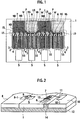
- Fig. 1 shows a plan view of an electrode structure of a semiconductor device according to a first embodiment of the present invention.
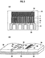
- Fig. 2 shows a perspective view for explaining a configuration of a part of the semiconductor device according to the first embodiment of the present invention.
- the semiconductor device includes: a main substrate 1; a plurality of source finger electrodes 3 disposed by determined direction on the main substrate 1; a plurality of drain finger electrodes 4 which are placed and are disposed a predetermined interval to a plurality of source finger electrodes 3, respectively; a plurality of gate finger electrodes 2 disposed between a plurality of source finger electrodes 3 and a plurality of drain finger electrodes 4; a plurality of source pads 6 which are placed and are disposed a predetermined interval at one side of a plurality of finger electrode array; a plurality of drain pads 7 disposed between a plurality of source pads 6; a plurality of gate pads 5 which are placed and are disposed a predetermined interval at the another side of a plurality of finger electrode arrays; source electrode wirings (source bus-line LS, source bridge-line NS and source bridge-line M), which connect the source finger electrode 3 of a prescribed number to a plurality
- the source bus-line LS, the source bridge-line NS and the source bridge-line M, and the drain bus-line LD, drain bridge-line ND, and drain bridge-line P have an overlay or an air bridge wiring part 15 over another side in one side.
- the semiconductor device includes: a input side matching circuit substrate 8 by which adjacent disposition is performed to the array side of a plurality of gate pads 5 placed on the main substrate 1; a wire 9 for connecting an output terminal 8-1 and the gate pad 5 on the input side matching circuit substrate 8; an output side matching circuit substrate 10 which is placed a predetermined interval at the array side of a plurality of source pads 6 and a plurality of drain pads 7 which are placed on the main substrate 1; a wire 11 for connecting an input terminal 10-1 and the drain pad 7 on the output side matching circuit substrate 10; a ground plate 12 which is placed in common with a backside of the main substrate 1, the input side matching circuit substrate 8, and the output side matching circuit substrate 10, and a part has an exposed part 14 exposed to the surface of the main substrate 1 through between the main substrate 1 and the output side matching circuit substrate 10; and a wire 13 for connecting the source pad 6 to the exposed part 14.
- the semiconductor device is a multi-finger type FET, and as shown in Fig. 1 , a plurality of source finger electrodes 3 and a plurality of drain finger electrodes 4 are disposed by turns on the main substrate 1. And, the one gate finger electrode 2 is placed between the arbitrary adjoining source finger electrode 3 and drain finger electrode 4 of a pair.
- the rectangular source pad 6 and drain pad 7 are disposed by turns along with the finger electrode array at one side of these each finger electrode array side, for example, the upper side of Fig. 1 .
- the rectangular gate pad 5 is disposed at another side of the finger electrode array, for example, the lower side of Fig. 1 .
- each of these gate pads 5, the source pads 6 and the drain pads 7, and each of the gate finger electrodes 2, the source finger electrodes 3 and the drain finger electrodes 4 are as follows.
- drain finger electrode 4 is also placed besides the source finger electrode 3 on the lower part of the source pad 6.
- source finger electrode 3 is also placed besides the drain finger electrode 4 on the lower part of the drain pad 7.
- connection between the source pad 6 and the source finger electrode 3 is performed as follows. That is, for example, the four source finger electrodes 3 disposed with the down side of the drain pad 7 within the limits of pad width in the direction of the finger electrode array are connected with those top ends in common through the source bus-line LS, and are connected to the source pads 6 of both sides of the drain pads 7 through the source electrode wirings M formed on the surface of the main substrate 1, in both of the right and left ends part of the source bus-line LS.
- the two source finger electrodes 3, disposed with the down side of the source pad 6 within the limits of pad width in the direction of the finger electrode array, are connected to the source pads 6 through the overlay source electrode wirings NS, respectively.
- connection between the drain pad 7 and the drain finger electrode 4 is performed as follows. That is, for example, three drain finger electrodes 4, disposed with the down side of the source pad 6 within the limits of pad width in the direction of the finger electrode array, are connected with those top ends in common through the drain bus-line LD extended and formed in the direction of the finger electrode array, and are connected to the drain pads 7 of both sides of the source pads 6 through the overlay drain bridge-line P, in both of the right and left ends part of the drain bus-line LD.
- three drain finger electrodes 4 disposed with the down side of the drain pads 7 within the limits of the pad width in the direction of the finger electrode array are connected to the drain pads 7 through the overlay drain bridge-lines ND, respectively.
- connection between the gate pad 5 and the gate finger electrode 2 is performed as follows. That is, the six continuous gate finger electrodes 2 are connected with those bottom ends in common through the gate bus-lines LG extended and formed in the direction of the finger electrode array, and are connected to the gate pads 5 in which the central part of the gate bus-lines LG is placed in the neighborhood.
- the metal ground plates 12 are formed on those backs with the substrate 1. And, between the substrate 1 and the output side substrate 10, the convex exposed part 14 exposed to those surfaces is formed on the ground plate 12.
- This ground plate 12 functions as common earth potentials for the circuit formed on the main substrate 1, the input side substrate 8, and the output side substrate 10.
- the gate pad 5 is provided on the input side of the main substrate 1, and is connected to the input matching circuit (output terminal 8-1) formed on the input side of the substrate 8 through the wire 9.
- the source pad 6 is connected to the exposed part 14 of the ground plate 12 through the wire 13.
- the drain pad 7 is connected to the output matching circuit (input terminal 10-1) formed on the output side of the substrate 10 through the wire 11, respectively.
- the semiconductor device can provide the exposed part 14 of the ground plate 12 in the output side instead of the input side of the FET by placing the source pad 6 to the same side as the drain pad 7 in the substrate 1, and, as a result, the length of the wire 9 which connects the gate pad 5 and the circuit on the input side of the substrate 8 can be shortened.
- the semiconductor device a part to which the wiringmember as the drain bus-line LD, the drain bridge-line ND, and the drain bridge-line P for connecting the drain pad 7 and the drain finger electrode 4 intersects the wiring member as the source bus-line LS, the source bridge-line NS and the source bridge-line M for connecting the source pad 6 and the source finger electrode 3, i. e. , the overlay or the air bridge wiring part 15 are placed near the source pad 6 and the drain pad 7.
- the overlay between the gate bus-lines LG and the drain bus-line LD, the drain bridge-line ND, and the drain bridge-line P, or the overlay between the gate bus-lines LG and the source bus-line LS, the source bridge-line NS and the source bridge-line M is not occurred.
- the stray capacity resulting from the overlap between the gate bus-lines LG and the drain bus-line LD, the drain bridge-line ND, and the drain bridge-line P, or the stray capacity resulting from the overlap between the gate bus-lines LG and the source bus-line LS, the source bridge-line NS and the source bridge-line M is not occurred.
- the semiconductor device also in a semiconductor element with difficult formation of the via hole, such as GaN (gallium nitride) and SiC (silicon carbide), it can form the grounding electrode.
- a semiconductor element with difficult formation of the via hole such as GaN (gallium nitride) and SiC (silicon carbide)
- the semiconductor device of low input inductance can be provided.
- Fig. 3 shows a plan view showing an electrode structure of a semiconductor device according to a second embodiment of the present invention.
- Fig. 4 shows a perspective view for explaining a configuration of a part of the semiconductor devices according to the second embodiment of the present invention.
- the semiconductor device includes: a main substrate 17; a plurality of source finger electrodes 3 disposed by determined direction on the main substrate 17; a plurality of drain finger electrodes 4 which are placed and are disposed a predetermined interval to a plurality of source finger electrodes 3, respectively; a plurality of gate finger electrodes 2 disposed between a plurality of source finger electrodes 3 and a plurality of drain finger electrodes 4; a plurality of source pads 6 which are placed and are disposed a predetermined interval at one side of a plurality of finger electrode array; a plurality of drain pads 7 disposed between a plurality of source pads 6; a plurality of gate pads 5 which are placed and are disposed a predetermined interval at the another side of a plurality of finger electrode arrays; source bus-line LS, source bridge-line NS and source bridge-line M which connect the source finger electrode 3 of a prescribed number to a plurality of source pads 6; drain
- the source bus-line LS, the source bridge-line NS and the source bridge-line M and the drain bus-line LD, the drain bridge-line ND, and the drain bridge-line P have an overlay or an air bridge wiring part 15 over another side in one side.
- the semiconductor device includes: an input side matching circuit substrate 8 by which adjacent disposition is performed to the array side of a plurality of gate pads 5 placed on the main substrate 17; a wire 9 which connects an output terminal 8-1 and the gate pad 5 on the input side matching circuit substrate 8; an output side matching circuit substrate 10 by which adjacent disposition is performed to the array side of a plurality of source pads 6 and a plurality of drain pads 7 which are placed on the main substrate 17; a wire 11 which connects an input terminal 10-1 and the drain pad 7 on the output side matching circuit substrate 10; a plurality of via holes 16 which pass through the main substrate 17 and are connected with a plurality of source pads 6, respectively; and a ground plate 12 which is placed common to a backside of the main substrate 17, the input side matching circuit substrate 8, and the output side matching circuit substrate 10, and is connected with a plurality of source pads 6 through a plurality of via holes 16.
- the source pad 6 is grounded by the exposed part 14 of the ground plate 12 through the wire 13 for bonding.
- the source pad 6 is connected to the ground plate 12 and is grounded, through the via hole 16 formed in the main substrate 17 under the source pad 6.
- Other configurations are the same as that of Fig. 1 and Fig. 2 .
- the wire length between the gate pad 5 and the gate finger electrode 2 can be shortened.
- the overlay with other source electrodes 3 and drain electrode 4 does not occur in the gate electrode 2, and therefore the stray capacity of the gate finger electrode 2 can also be made small, the influence on the frequency characteristic of the FET can be made small.
- the semiconductor device of low input inductance can be provided.
- the present invention is not limited to the above-mentioned embodiments as they are, and therefore shape can be taken by modifying components in an implementation phase in the scope which does not deviate from the gist.
- the order of the source pad 6 and the drain pad 7 may be replaced, and in this case, the order of the source finger 3 and the drain finger 4 is also replaced.
- Various values such as the length of the side of the main substrates 1 and 17, the length of each finger and the interval of arrangement, the length of the side of each pad and the interval of arrangement, the structure of the overlap of the wiring member in the overlay or the air bridge wiring part 15, and the diameter of the via hole 16, in the above-mentioned explanation, can be changed.
- various inventions can be formed with a proper combination of a plurality of components currently disclosed by the above-mentioned embodiment. For example, some components may be eliminated from all the components shown in the embodiments. Furthermore, the component covering a different embodiment may be combined suitably.
- the SiC substrate is mentioned as the main substrates 1 and 17 used for the semiconductor element, it is not limited to this.
- a satisfactory substrate of heat radiation characteristics such as a GaN/SiC substrate, an AlGaN/GaN/SiC substrate, and a diamond substrate, it is possible to ground by formation of the via hole 16.
- processing for formation of the via hole is easy, but it is also effective to apply also when processing for formation of via hole, such as a SiC substrate and a sapphire substrate, uses a difficult substrate.
Landscapes
- Junction Field-Effect Transistors (AREA)
Claims (4)
- Dispositif semi-conducteur comprenant :une pluralité d'électrodes sources digitées (3) agencées sur le substrat principal dans une direction prédéterminée ;une pluralité d'électrodes drains digitées (4), les électrodes drains digitées respectives et les électrodes sources digitées respectives étant agencées de manière alternée les unes par rapport aux autres, dans la direction prédéterminée ;une pluralité d'électrodes de grille digitées (2), les électrodes de grille digitées respectives étant agencées entre les électrodes sources digitées respectives et les électrodes drains digitées respectives, dans la direction prédéterminée ;ladite pluralité d'électrodes sources, drains et de grille digitées formant un réseau d'électrodes digitées ;une pluralité de pastilles de source (6) agencées au niveau de seulement un côté dudit réseau d'électrodes digitées ;une pluralité de pastilles de drain (7) agencées seulement sur ledit un côté et entre la pluralité de pastilles de source ;une pluralité de pastilles de grille (5) agencées au niveau de seulement le côté opposé dudit réseau d'électrodes digitées ;pour chaque pastille de source, un câblage d'électrode source raccordant un nombre prédéterminé des électrodes sources digitées à la pastille de source respective ;
pour chaque pastille de drain, un câblage d'électrode drain raccordant un nombre prédéterminé des électrodes drains digitées à la pastille de drain respective ; et
pour chaque pastille de grille, un câblage d'électrode de grille raccordant un nombre prédéterminé des électrodes de grille digitées à la pastille de grille respective,
dans lequel le câblage d'électrode source comprend un premier câblage d'électrode source (LS, M) et un second câblage d'électrode source (NS), et le câblage d'électrode drain comprend un premier câblage d'électrode drain (LD, P) et un second câblage d'électrode drain (ND),
dans lequel le second câblage d'électrode source (NS) et le second câblage d'électrode drain (ND) présentent un câblage de revêtement ou de pont aérien configuré de telle manière que le second câblage d'électrode source (NS) chevauche un premier câblage d'électrode drain (LD) et le second câblage d'électrode drain (ND) chevauche un premier câblage d'électrode source (LS),
dans lequel le premier câblage d'électrode source (LS) est agencé au niveau d'une position correspondant à chaque pastille de drain (7), les électrodes sources digitées (3) en réseau dans une plage correspondant à une largeur de chaque pastille de drain (7) dans une direction de réseau des électrodes sources digitées (3) sont raccordées en commun avec le premier câblage d'électrode source (LS) agencé au niveau de la position correspondant à chaque pastille de drain (7), et les deux extrémités du premier câblage d'électrode source (LS) sont raccordées aux pastilles de source (6) agencées au niveau des deux côtés de la pastille de drain (7) correspondante,
dans lequel le premier câblage d'électrode drain (LD) est agencé au niveau d'une position correspondant à chaque pastille de source (6), les électrodes drains digitées (4) en réseau dans une plage correspondant à une largeur de chaque pastille de source (6) dans une direction de réseau des électrodes drains digitées (4) sont raccordées en commun avec le premier câblage d'électrode drain (LD) agencé au niveau de la position correspondant à chaque pastille de source (6), les deux extrémités du premier câblage d'électrode drain (LD) sont raccordées aux pastilles de drain agencées au niveau des deux côtés de la pastille de source (6) correspondante,
dans lequel les électrodes sources digitées (3) en réseau dans la plage correspondant à la largeur de chaque pastille de source (6) dans la direction de réseau des électrodes sources digitées (3) sont raccordées aux pastilles de source (6) avec le câblage de revêtement ou de pont aérien du second câblage d'électrode source (NS), et
les électrodes drains digitées (4) en réseau dans la plage correspondant à la largeur de chaque pastille de drain (7) dans la direction de réseau des électrodes drains digitées (4) sont raccordées aux pastilles de drain (7) avec le câblage de revêtement ou de pont aérien du second câblage d'électrode drain (ND). - Dispositif semi-conducteur selon la revendication 1, comprenant en outre :un substrat de circuit d'adaptation côté entrée (8) agencé adjacent au substrat principal sur le côté présentant les pastilles de grille ;un premier câble (9) qui raccorde une borne de sortie (8-1) sur le substrat de circuit d'adaptation côté entrée à la pastille de grille respective ;un substrat de circuit d'adaptation côté sortie (10) agencé adjacent au substrat principal sur le côté opposé présentant les pastilles de source et de drain de manière à laisser un espace prédéterminé (14) entre les substrats ;un deuxième câble (11) qui raccorde une entrée (10-1) sur le substrat de circuit d'adaptation côté sortie à la pastille de drain respective ;une plaque de terre (12) agencée sur des côtés arrière respectifs du substrat principal, du substrat de circuit d'adaptation côté entrée et du substrat de circuit d'adaptation côté sortie, et présentant une partie exposée (14) de la plaque de terre exposée entre le substrat principal et le substrat de circuit d'adaptation côté sortie ; etun troisième câble (13) qui raccorde la pastille de source respective à la partie exposée.
- Dispositif semi-conducteur selon la revendication 1, comprenant en outre :un substrat de circuit d'adaptation côté entrée (8) agencé adjacent au substrat principal sur le côté présentant les pastilles de grille ;un premier câble (9) qui raccorde une borne de sortie (8-1) sur le substrat de circuit d'adaptation côté entrée à la pastille de grille respective ;un substrat de circuit d'adaptation côté sortie (10) agencé adjacent au substrat principal sur le côté opposé présentant les pastilles de source et de drain ;un deuxième câble (11) qui raccorde une borne d'entrée (10-1) sur le substrat de circuit d'adaptation côté sortie à la pastille de drain respective ;une pluralité de trous traversants (16) qui passent à travers le substrat principal et sont raccordés à la pluralité de pastilles de source, respectivement ; etune plaque de terre (12) agencée sur un côté arrière respectif du substrat principal, du substrat de circuit d'adaptation côté entrée et du substrat de circuit d'adaptation côté sortie, et raccordée à la pluralité de pastilles de source à travers la pluralité de trous traversants, respectivement.
- Dispositif semi-conducteur selon la revendication 1, dans lequel le substrat principal est un substrat sélectionné parmi un substrat SiC, un substrat GaN/SiC, un substrat AlGaN/GaN/SiC, un substrat au diamant, et un substrat au saphir.
Applications Claiming Priority (2)
| Application Number | Priority Date | Filing Date | Title |
|---|---|---|---|
| JP2006298820 | 2006-11-02 | ||
| PCT/JP2007/070640 WO2008053748A1 (fr) | 2006-11-02 | 2007-10-23 | Dispositif semiconducteur |
Publications (3)
| Publication Number | Publication Date |
|---|---|
| EP2088620A1 EP2088620A1 (fr) | 2009-08-12 |
| EP2088620A4 EP2088620A4 (fr) | 2011-11-30 |
| EP2088620B1 true EP2088620B1 (fr) | 2016-03-16 |
Family
ID=39344091
Family Applications (1)
| Application Number | Title | Priority Date | Filing Date |
|---|---|---|---|
| EP07830374.0A Not-in-force EP2088620B1 (fr) | 2006-11-02 | 2007-10-23 | Dispositif semiconducteur |
Country Status (6)
| Country | Link |
|---|---|
| US (1) | US8097906B2 (fr) |
| EP (1) | EP2088620B1 (fr) |
| JP (1) | JP5127721B2 (fr) |
| KR (1) | KR20090004978A (fr) |
| TW (1) | TW200830549A (fr) |
| WO (1) | WO2008053748A1 (fr) |
Families Citing this family (27)
| Publication number | Priority date | Publication date | Assignee | Title |
|---|---|---|---|---|
| JP4995890B2 (ja) * | 2009-12-25 | 2012-08-08 | 株式会社東芝 | 半導体装置及びdc−dcコンバータ |
| US8319256B2 (en) * | 2010-06-23 | 2012-11-27 | Power Integrations, Inc. | Layout design for a high power, GaN-based FET |
| US9236378B2 (en) | 2010-08-11 | 2016-01-12 | Sarda Technologies, Inc. | Integrated switch devices |
| US8896034B1 (en) | 2010-08-11 | 2014-11-25 | Sarda Technologies, Inc. | Radio frequency and microwave devices and methods of use |
| US8519916B2 (en) * | 2010-08-11 | 2013-08-27 | Sarda Technologies, Inc. | Low interconnect resistance integrated switches |
| JP2012175070A (ja) * | 2011-02-24 | 2012-09-10 | Panasonic Corp | 半導体パッケージ |
| JP5361934B2 (ja) * | 2011-04-19 | 2013-12-04 | 株式会社東芝 | 電力増幅器 |
| CN102270659B (zh) * | 2011-08-11 | 2012-09-26 | 中国科学院微电子研究所 | 一种多栅指GaN HEMTs |
| JP5443519B2 (ja) * | 2012-01-16 | 2014-03-19 | 株式会社東芝 | 半導体装置及びdc−dcコンバータ |
| JP5443520B2 (ja) * | 2012-01-16 | 2014-03-19 | 株式会社東芝 | 半導体装置及びdc−dcコンバータ |
| JP5444383B2 (ja) * | 2012-01-16 | 2014-03-19 | 株式会社東芝 | 半導体装置及びdc−dcコンバータ |
| JP2013183061A (ja) * | 2012-03-02 | 2013-09-12 | Toshiba Corp | 半導体装置 |
| JP5985282B2 (ja) * | 2012-07-12 | 2016-09-06 | ルネサスエレクトロニクス株式会社 | 半導体装置 |
| CN103633046B (zh) * | 2013-12-13 | 2017-03-15 | 苏州能讯高能半导体有限公司 | 半导体器件及其制造方法 |
| CN103928525A (zh) * | 2014-04-25 | 2014-07-16 | 中国科学院微电子研究所 | 场效应晶体管液体传感器及其制备方法 |
| US9774322B1 (en) | 2016-06-22 | 2017-09-26 | Sarda Technologies, Inc. | Gate driver for depletion-mode transistors |
| EP3474316B1 (fr) * | 2016-07-25 | 2021-03-03 | Mitsubishi Electric Corporation | Dispositif à semi-conducteurs |
| US10545055B2 (en) | 2017-06-13 | 2020-01-28 | Semiconductor Components Industries, Llc | Electronic device including a temperature sensor |
| CN107083994B (zh) | 2017-06-16 | 2023-03-24 | 传孚科技(厦门)有限公司 | 气压发动机 |
| US10629526B1 (en) * | 2018-10-11 | 2020-04-21 | Nxp Usa, Inc. | Transistor with non-circular via connections in two orientations |
| WO2020202600A1 (fr) * | 2019-03-29 | 2020-10-08 | 株式会社 東芝 | Dispositif à semi-conducteur et procédé de fabrication de dispositif à semi-conducteur |
| CA3114695A1 (fr) | 2020-04-08 | 2021-10-08 | National Research Council Of Canada | Structure de transistor a effet de champ integree a inductance distribuee |
| WO2022021164A1 (fr) * | 2020-07-29 | 2022-02-03 | 华为技术有限公司 | Structure semi-conductrice, dispositif électronique et procédé de préparation de structure semi-conductrice |
| US11145579B1 (en) | 2020-09-11 | 2021-10-12 | Navitas Semiconductor Limited | Thermally enhanced electronic packages for GaN power integrated circuits |
| US11715720B2 (en) * | 2020-09-11 | 2023-08-01 | Navitas Semiconductor Limited | Integrated half-bridge power converter |
| EP4264666A1 (fr) * | 2021-01-11 | 2023-10-25 | Huawei Technologies Co., Ltd. | Transistor de puissance multi-terminal au nitrure de gallium |
| JP7596868B2 (ja) * | 2021-03-15 | 2024-12-10 | 住友電気工業株式会社 | 半導体装置および電力増幅器 |
Family Cites Families (11)
| Publication number | Priority date | Publication date | Assignee | Title |
|---|---|---|---|---|
| JP2554672B2 (ja) | 1987-10-09 | 1996-11-13 | 株式会社東芝 | 電界効果型半導体装置 |
| JPH03150851A (ja) * | 1989-11-08 | 1991-06-27 | Hitachi Ltd | 高利得半導体素子電極構造 |
| JPH06209015A (ja) | 1992-10-26 | 1994-07-26 | Kobe Steel Ltd | ダイヤモンド接合型電界効果トランジスタ及びその製造方法 |
| JPH07226489A (ja) | 1994-02-15 | 1995-08-22 | Toshiba Corp | マイクロ波半導体装置 |
| JP3150851B2 (ja) | 1994-07-08 | 2001-03-26 | 三晃金属工業株式会社 | 彎曲状外囲体 |
| DE19522364C1 (de) * | 1995-06-20 | 1996-07-04 | Siemens Ag | Halbleiter-Bauelement |
| JP3499103B2 (ja) * | 1997-02-21 | 2004-02-23 | 三菱電機株式会社 | 半導体装置 |
| JP3147048B2 (ja) | 1997-09-12 | 2001-03-19 | 日本電気株式会社 | 半導体装置 |
| JP3114687B2 (ja) | 1998-03-30 | 2000-12-04 | 日本電気株式会社 | 半導体装置 |
| JP2002319593A (ja) | 2001-04-19 | 2002-10-31 | Furukawa Electric Co Ltd:The | 半導体デバイスおよび電極形成方法 |
| JP4439358B2 (ja) * | 2003-09-05 | 2010-03-24 | 株式会社東芝 | 電界効果トランジスタ及びその製造方法 |
-
2007
- 2007-10-23 US US12/294,620 patent/US8097906B2/en not_active Expired - Fee Related
- 2007-10-23 JP JP2008542057A patent/JP5127721B2/ja not_active Expired - Fee Related
- 2007-10-23 WO PCT/JP2007/070640 patent/WO2008053748A1/fr not_active Ceased
- 2007-10-23 KR KR1020087025180A patent/KR20090004978A/ko not_active Ceased
- 2007-10-23 EP EP07830374.0A patent/EP2088620B1/fr not_active Not-in-force
- 2007-11-01 TW TW096141191A patent/TW200830549A/zh not_active IP Right Cessation
Also Published As
| Publication number | Publication date |
|---|---|
| WO2008053748A1 (fr) | 2008-05-08 |
| TW200830549A (en) | 2008-07-16 |
| US20100237437A1 (en) | 2010-09-23 |
| EP2088620A4 (fr) | 2011-11-30 |
| US8097906B2 (en) | 2012-01-17 |
| JP5127721B2 (ja) | 2013-01-23 |
| JPWO2008053748A1 (ja) | 2010-02-25 |
| TWI355741B (fr) | 2012-01-01 |
| KR20090004978A (ko) | 2009-01-12 |
| EP2088620A1 (fr) | 2009-08-12 |
Similar Documents
| Publication | Publication Date | Title |
|---|---|---|
| EP2088620B1 (fr) | Dispositif semiconducteur | |
| JP3712111B2 (ja) | 電力増幅用半導体装置 | |
| JP2005183770A (ja) | 高周波用半導体装置 | |
| JP2001028425A (ja) | 半導体装置及びその製造方法 | |
| KR20200062938A (ko) | 스택된 전계효과트랜지스터(fet)를 갖는 반도체 디바이스 | |
| CN116646350A (zh) | 半导体装置 | |
| US6727559B2 (en) | Compound semiconductor device | |
| CN101371345B (zh) | 高频用半导体器件 | |
| JP4133600B2 (ja) | 半導体装置 | |
| US9472497B2 (en) | Semiconductor device | |
| KR100742067B1 (ko) | 반도체 장치 | |
| US9786640B2 (en) | Transistor arrangement | |
| JP2010245351A (ja) | 半導体装置 | |
| CN106024891B (zh) | 包括辅助沟槽结构的半导体器件和集成电路 | |
| US12464800B2 (en) | Semiconductor device | |
| JP2022135898A (ja) | 半導体装置 | |
| US10290583B2 (en) | Semiconductor device | |
| JP3171155B2 (ja) | 半導体装置及びその製造方法 | |
| CN115036309A (zh) | 半导体装置 | |
| CN120642594A (zh) | 半导体装置 | |
| JPH06342813A (ja) | 電界効果トランジスタ | |
| JP2014175408A (ja) | 半導体装置 | |
| KR20180103470A (ko) | 반도체 소자 및 반도체 소자를 이용한 장치 | |
| JP2015002330A (ja) | 窒化物半導体装置 |
Legal Events
| Date | Code | Title | Description |
|---|---|---|---|
| PUAI | Public reference made under article 153(3) epc to a published international application that has entered the european phase |
Free format text: ORIGINAL CODE: 0009012 |
|
| 17P | Request for examination filed |
Effective date: 20081010 |
|
| AK | Designated contracting states |
Kind code of ref document: A1 Designated state(s): AT BE BG CH CY CZ DE DK EE ES FI FR GB GR HU IE IS IT LI LT LU LV MC MT NL PL PT RO SE SI SK TR |
|
| DAX | Request for extension of the european patent (deleted) | ||
| A4 | Supplementary search report drawn up and despatched |
Effective date: 20111102 |
|
| RIC1 | Information provided on ipc code assigned before grant |
Ipc: H01L 23/66 20060101ALI20111026BHEP Ipc: H01L 21/338 20060101AFI20111026BHEP Ipc: H01L 23/482 20060101ALI20111026BHEP Ipc: H01L 29/812 20060101ALI20111026BHEP |
|
| 17Q | First examination report despatched |
Effective date: 20120928 |
|
| REG | Reference to a national code |
Ref country code: DE Ref legal event code: R079 Ref document number: 602007045336 Country of ref document: DE Free format text: PREVIOUS MAIN CLASS: H01L0021338000 Ipc: H01L0023490000 |
|
| RIC1 | Information provided on ipc code assigned before grant |
Ipc: H01L 29/812 20060101ALI20150703BHEP Ipc: H01L 23/482 20060101ALI20150703BHEP Ipc: H01L 23/66 20060101ALI20150703BHEP Ipc: H01L 21/338 20060101ALI20150703BHEP Ipc: H01L 23/49 20060101AFI20150703BHEP |
|
| GRAP | Despatch of communication of intention to grant a patent |
Free format text: ORIGINAL CODE: EPIDOSNIGR1 |
|
| INTG | Intention to grant announced |
Effective date: 20151007 |
|
| RIN1 | Information on inventor provided before grant (corrected) |
Inventor name: TAKAGI, KAZUTAKA |
|
| GRAS | Grant fee paid |
Free format text: ORIGINAL CODE: EPIDOSNIGR3 |
|
| GRAA | (expected) grant |
Free format text: ORIGINAL CODE: 0009210 |
|
| AK | Designated contracting states |
Kind code of ref document: B1 Designated state(s): AT BE BG CH CY CZ DE DK EE ES FI FR GB GR HU IE IS IT LI LT LU LV MC MT NL PL PT RO SE SI SK TR |
|
| REG | Reference to a national code |
Ref country code: GB Ref legal event code: FG4D |
|
| REG | Reference to a national code |
Ref country code: CH Ref legal event code: EP |
|
| REG | Reference to a national code |
Ref country code: IE Ref legal event code: FG4D |
|
| REG | Reference to a national code |
Ref country code: AT Ref legal event code: REF Ref document number: 781887 Country of ref document: AT Kind code of ref document: T Effective date: 20160415 |
|
| REG | Reference to a national code |
Ref country code: DE Ref legal event code: R096 Ref document number: 602007045336 Country of ref document: DE |
|
| REG | Reference to a national code |
Ref country code: NL Ref legal event code: MP Effective date: 20160316 |
|
| REG | Reference to a national code |
Ref country code: LT Ref legal event code: MG4D |
|
| PG25 | Lapsed in a contracting state [announced via postgrant information from national office to epo] |
Ref country code: FI Free format text: LAPSE BECAUSE OF FAILURE TO SUBMIT A TRANSLATION OF THE DESCRIPTION OR TO PAY THE FEE WITHIN THE PRESCRIBED TIME-LIMIT Effective date: 20160316 Ref country code: GR Free format text: LAPSE BECAUSE OF FAILURE TO SUBMIT A TRANSLATION OF THE DESCRIPTION OR TO PAY THE FEE WITHIN THE PRESCRIBED TIME-LIMIT Effective date: 20160617 |
|
| REG | Reference to a national code |
Ref country code: AT Ref legal event code: MK05 Ref document number: 781887 Country of ref document: AT Kind code of ref document: T Effective date: 20160316 |
|
| PG25 | Lapsed in a contracting state [announced via postgrant information from national office to epo] |
Ref country code: NL Free format text: LAPSE BECAUSE OF FAILURE TO SUBMIT A TRANSLATION OF THE DESCRIPTION OR TO PAY THE FEE WITHIN THE PRESCRIBED TIME-LIMIT Effective date: 20160316 Ref country code: LT Free format text: LAPSE BECAUSE OF FAILURE TO SUBMIT A TRANSLATION OF THE DESCRIPTION OR TO PAY THE FEE WITHIN THE PRESCRIBED TIME-LIMIT Effective date: 20160316 Ref country code: SE Free format text: LAPSE BECAUSE OF FAILURE TO SUBMIT A TRANSLATION OF THE DESCRIPTION OR TO PAY THE FEE WITHIN THE PRESCRIBED TIME-LIMIT Effective date: 20160316 Ref country code: LV Free format text: LAPSE BECAUSE OF FAILURE TO SUBMIT A TRANSLATION OF THE DESCRIPTION OR TO PAY THE FEE WITHIN THE PRESCRIBED TIME-LIMIT Effective date: 20160316 |
|
| REG | Reference to a national code |
Ref country code: FR Ref legal event code: PLFP Year of fee payment: 10 |
|
| PG25 | Lapsed in a contracting state [announced via postgrant information from national office to epo] |
Ref country code: EE Free format text: LAPSE BECAUSE OF FAILURE TO SUBMIT A TRANSLATION OF THE DESCRIPTION OR TO PAY THE FEE WITHIN THE PRESCRIBED TIME-LIMIT Effective date: 20160316 Ref country code: IS Free format text: LAPSE BECAUSE OF FAILURE TO SUBMIT A TRANSLATION OF THE DESCRIPTION OR TO PAY THE FEE WITHIN THE PRESCRIBED TIME-LIMIT Effective date: 20160716 Ref country code: PL Free format text: LAPSE BECAUSE OF FAILURE TO SUBMIT A TRANSLATION OF THE DESCRIPTION OR TO PAY THE FEE WITHIN THE PRESCRIBED TIME-LIMIT Effective date: 20160316 |
|
| PG25 | Lapsed in a contracting state [announced via postgrant information from national office to epo] |
Ref country code: CZ Free format text: LAPSE BECAUSE OF FAILURE TO SUBMIT A TRANSLATION OF THE DESCRIPTION OR TO PAY THE FEE WITHIN THE PRESCRIBED TIME-LIMIT Effective date: 20160316 Ref country code: AT Free format text: LAPSE BECAUSE OF FAILURE TO SUBMIT A TRANSLATION OF THE DESCRIPTION OR TO PAY THE FEE WITHIN THE PRESCRIBED TIME-LIMIT Effective date: 20160316 Ref country code: SK Free format text: LAPSE BECAUSE OF FAILURE TO SUBMIT A TRANSLATION OF THE DESCRIPTION OR TO PAY THE FEE WITHIN THE PRESCRIBED TIME-LIMIT Effective date: 20160316 Ref country code: RO Free format text: LAPSE BECAUSE OF FAILURE TO SUBMIT A TRANSLATION OF THE DESCRIPTION OR TO PAY THE FEE WITHIN THE PRESCRIBED TIME-LIMIT Effective date: 20160316 Ref country code: ES Free format text: LAPSE BECAUSE OF FAILURE TO SUBMIT A TRANSLATION OF THE DESCRIPTION OR TO PAY THE FEE WITHIN THE PRESCRIBED TIME-LIMIT Effective date: 20160316 Ref country code: PT Free format text: LAPSE BECAUSE OF FAILURE TO SUBMIT A TRANSLATION OF THE DESCRIPTION OR TO PAY THE FEE WITHIN THE PRESCRIBED TIME-LIMIT Effective date: 20160718 |
|
| PGFP | Annual fee paid to national office [announced via postgrant information from national office to epo] |
Ref country code: FR Payment date: 20160919 Year of fee payment: 10 |
|
| REG | Reference to a national code |
Ref country code: DE Ref legal event code: R097 Ref document number: 602007045336 Country of ref document: DE |
|
| PG25 | Lapsed in a contracting state [announced via postgrant information from national office to epo] |
Ref country code: BE Free format text: LAPSE BECAUSE OF FAILURE TO SUBMIT A TRANSLATION OF THE DESCRIPTION OR TO PAY THE FEE WITHIN THE PRESCRIBED TIME-LIMIT Effective date: 20160316 Ref country code: IT Free format text: LAPSE BECAUSE OF FAILURE TO SUBMIT A TRANSLATION OF THE DESCRIPTION OR TO PAY THE FEE WITHIN THE PRESCRIBED TIME-LIMIT Effective date: 20160316 |
|
| PLBE | No opposition filed within time limit |
Free format text: ORIGINAL CODE: 0009261 |
|
| STAA | Information on the status of an ep patent application or granted ep patent |
Free format text: STATUS: NO OPPOSITION FILED WITHIN TIME LIMIT |
|
| PG25 | Lapsed in a contracting state [announced via postgrant information from national office to epo] |
Ref country code: DK Free format text: LAPSE BECAUSE OF FAILURE TO SUBMIT A TRANSLATION OF THE DESCRIPTION OR TO PAY THE FEE WITHIN THE PRESCRIBED TIME-LIMIT Effective date: 20160316 |
|
| 26N | No opposition filed |
Effective date: 20161219 |
|
| PG25 | Lapsed in a contracting state [announced via postgrant information from national office to epo] |
Ref country code: BG Free format text: LAPSE BECAUSE OF FAILURE TO SUBMIT A TRANSLATION OF THE DESCRIPTION OR TO PAY THE FEE WITHIN THE PRESCRIBED TIME-LIMIT Effective date: 20160616 |
|
| REG | Reference to a national code |
Ref country code: DE Ref legal event code: R119 Ref document number: 602007045336 Country of ref document: DE |
|
| PG25 | Lapsed in a contracting state [announced via postgrant information from national office to epo] |
Ref country code: SI Free format text: LAPSE BECAUSE OF FAILURE TO SUBMIT A TRANSLATION OF THE DESCRIPTION OR TO PAY THE FEE WITHIN THE PRESCRIBED TIME-LIMIT Effective date: 20160316 |
|
| REG | Reference to a national code |
Ref country code: CH Ref legal event code: PL |
|
| GBPC | Gb: european patent ceased through non-payment of renewal fee |
Effective date: 20161023 |
|
| REG | Reference to a national code |
Ref country code: IE Ref legal event code: MM4A |
|
| PG25 | Lapsed in a contracting state [announced via postgrant information from national office to epo] |
Ref country code: DE Free format text: LAPSE BECAUSE OF NON-PAYMENT OF DUE FEES Effective date: 20170503 Ref country code: GB Free format text: LAPSE BECAUSE OF NON-PAYMENT OF DUE FEES Effective date: 20161023 Ref country code: CH Free format text: LAPSE BECAUSE OF NON-PAYMENT OF DUE FEES Effective date: 20161031 Ref country code: LI Free format text: LAPSE BECAUSE OF NON-PAYMENT OF DUE FEES Effective date: 20161031 |
|
| PG25 | Lapsed in a contracting state [announced via postgrant information from national office to epo] |
Ref country code: LU Free format text: LAPSE BECAUSE OF NON-PAYMENT OF DUE FEES Effective date: 20161023 |
|
| PG25 | Lapsed in a contracting state [announced via postgrant information from national office to epo] |
Ref country code: IE Free format text: LAPSE BECAUSE OF NON-PAYMENT OF DUE FEES Effective date: 20161023 |
|
| PG25 | Lapsed in a contracting state [announced via postgrant information from national office to epo] |
Ref country code: CY Free format text: LAPSE BECAUSE OF FAILURE TO SUBMIT A TRANSLATION OF THE DESCRIPTION OR TO PAY THE FEE WITHIN THE PRESCRIBED TIME-LIMIT Effective date: 20160316 Ref country code: HU Free format text: LAPSE BECAUSE OF FAILURE TO SUBMIT A TRANSLATION OF THE DESCRIPTION OR TO PAY THE FEE WITHIN THE PRESCRIBED TIME-LIMIT; INVALID AB INITIO Effective date: 20071023 |
|
| PG25 | Lapsed in a contracting state [announced via postgrant information from national office to epo] |
Ref country code: TR Free format text: LAPSE BECAUSE OF FAILURE TO SUBMIT A TRANSLATION OF THE DESCRIPTION OR TO PAY THE FEE WITHIN THE PRESCRIBED TIME-LIMIT Effective date: 20160316 Ref country code: MT Free format text: LAPSE BECAUSE OF NON-PAYMENT OF DUE FEES Effective date: 20161031 Ref country code: MC Free format text: LAPSE BECAUSE OF FAILURE TO SUBMIT A TRANSLATION OF THE DESCRIPTION OR TO PAY THE FEE WITHIN THE PRESCRIBED TIME-LIMIT Effective date: 20160316 |
|
| REG | Reference to a national code |
Ref country code: FR Ref legal event code: ST Effective date: 20180629 |
|
| PG25 | Lapsed in a contracting state [announced via postgrant information from national office to epo] |
Ref country code: FR Free format text: LAPSE BECAUSE OF NON-PAYMENT OF DUE FEES Effective date: 20171031 |