EP2090966B1 - Kapazitiver Berührungsbildschirm - Google Patents
Kapazitiver Berührungsbildschirm Download PDFInfo
- Publication number
- EP2090966B1 EP2090966B1 EP08155297A EP08155297A EP2090966B1 EP 2090966 B1 EP2090966 B1 EP 2090966B1 EP 08155297 A EP08155297 A EP 08155297A EP 08155297 A EP08155297 A EP 08155297A EP 2090966 B1 EP2090966 B1 EP 2090966B1
- Authority
- EP
- European Patent Office
- Prior art keywords
- layer
- sensing circuit
- touch panel
- circuit layer
- lens
- Prior art date
- Legal status (The legal status is an assumption and is not a legal conclusion. Google has not performed a legal analysis and makes no representation as to the accuracy of the status listed.)
- Active
Links
Images


Classifications
-
- G—PHYSICS
- G06—COMPUTING OR CALCULATING; COUNTING
- G06F—ELECTRIC DIGITAL DATA PROCESSING
- G06F3/00—Input arrangements for transferring data to be processed into a form capable of being handled by the computer; Output arrangements for transferring data from processing unit to output unit, e.g. interface arrangements
- G06F3/01—Input arrangements or combined input and output arrangements for interaction between user and computer
- G06F3/03—Arrangements for converting the position or the displacement of a member into a coded form
- G06F3/041—Digitisers, e.g. for touch screens or touch pads, characterised by the transducing means
- G06F3/044—Digitisers, e.g. for touch screens or touch pads, characterised by the transducing means by capacitive means
- G06F3/0443—Digitisers, e.g. for touch screens or touch pads, characterised by the transducing means by capacitive means using a single layer of sensing electrodes
-
- G—PHYSICS
- G06—COMPUTING OR CALCULATING; COUNTING
- G06F—ELECTRIC DIGITAL DATA PROCESSING
- G06F3/00—Input arrangements for transferring data to be processed into a form capable of being handled by the computer; Output arrangements for transferring data from processing unit to output unit, e.g. interface arrangements
- G06F3/01—Input arrangements or combined input and output arrangements for interaction between user and computer
- G06F3/03—Arrangements for converting the position or the displacement of a member into a coded form
- G06F3/041—Digitisers, e.g. for touch screens or touch pads, characterised by the transducing means
- G06F3/0412—Digitisers structurally integrated in a display
-
- G—PHYSICS
- G02—OPTICS
- G02F—OPTICAL DEVICES OR ARRANGEMENTS FOR THE CONTROL OF LIGHT BY MODIFICATION OF THE OPTICAL PROPERTIES OF THE MEDIA OF THE ELEMENTS INVOLVED THEREIN; NON-LINEAR OPTICS; FREQUENCY-CHANGING OF LIGHT; OPTICAL LOGIC ELEMENTS; OPTICAL ANALOGUE/DIGITAL CONVERTERS
- G02F1/00—Devices or arrangements for the control of the intensity, colour, phase, polarisation or direction of light arriving from an independent light source, e.g. switching, gating or modulating; Non-linear optics
- G02F1/01—Devices or arrangements for the control of the intensity, colour, phase, polarisation or direction of light arriving from an independent light source, e.g. switching, gating or modulating; Non-linear optics for the control of the intensity, phase, polarisation or colour
- G02F1/13—Devices or arrangements for the control of the intensity, colour, phase, polarisation or direction of light arriving from an independent light source, e.g. switching, gating or modulating; Non-linear optics for the control of the intensity, phase, polarisation or colour based on liquid crystals, e.g. single liquid crystal display cells
- G02F1/133—Constructional arrangements; Operation of liquid crystal cells; Circuit arrangements
- G02F1/1333—Constructional arrangements; Manufacturing methods
- G02F1/13338—Input devices, e.g. touch panels
-
- G—PHYSICS
- G06—COMPUTING OR CALCULATING; COUNTING
- G06F—ELECTRIC DIGITAL DATA PROCESSING
- G06F1/00—Details not covered by groups G06F3/00 - G06F13/00 and G06F21/00
- G06F1/16—Constructional details or arrangements
- G06F1/1613—Constructional details or arrangements for portable computers
- G06F1/1633—Constructional details or arrangements of portable computers not specific to the type of enclosures covered by groups G06F1/1615 - G06F1/1626
- G06F1/1637—Details related to the display arrangement, including those related to the mounting of the display in the housing
- G06F1/1643—Details related to the display arrangement, including those related to the mounting of the display in the housing the display being associated to a digitizer, e.g. laptops that can be used as penpads
-
- G—PHYSICS
- G06—COMPUTING OR CALCULATING; COUNTING
- G06F—ELECTRIC DIGITAL DATA PROCESSING
- G06F3/00—Input arrangements for transferring data to be processed into a form capable of being handled by the computer; Output arrangements for transferring data from processing unit to output unit, e.g. interface arrangements
- G06F3/01—Input arrangements or combined input and output arrangements for interaction between user and computer
- G06F3/03—Arrangements for converting the position or the displacement of a member into a coded form
- G06F3/041—Digitisers, e.g. for touch screens or touch pads, characterised by the transducing means
-
- G—PHYSICS
- G06—COMPUTING OR CALCULATING; COUNTING
- G06F—ELECTRIC DIGITAL DATA PROCESSING
- G06F3/00—Input arrangements for transferring data to be processed into a form capable of being handled by the computer; Output arrangements for transferring data from processing unit to output unit, e.g. interface arrangements
- G06F3/01—Input arrangements or combined input and output arrangements for interaction between user and computer
- G06F3/03—Arrangements for converting the position or the displacement of a member into a coded form
- G06F3/041—Digitisers, e.g. for touch screens or touch pads, characterised by the transducing means
- G06F3/044—Digitisers, e.g. for touch screens or touch pads, characterised by the transducing means by capacitive means
- G06F3/0445—Digitisers, e.g. for touch screens or touch pads, characterised by the transducing means by capacitive means using two or more layers of sensing electrodes, e.g. using two layers of electrodes separated by a dielectric layer
-
- G—PHYSICS
- G06—COMPUTING OR CALCULATING; COUNTING
- G06F—ELECTRIC DIGITAL DATA PROCESSING
- G06F2203/00—Indexing scheme relating to G06F3/00 - G06F3/048
- G06F2203/041—Indexing scheme relating to G06F3/041 - G06F3/045
- G06F2203/04111—Cross over in capacitive digitiser, i.e. details of structures for connecting electrodes of the sensing pattern where the connections cross each other, e.g. bridge structures comprising an insulating layer, or vias through substrate
-
- G—PHYSICS
- G06—COMPUTING OR CALCULATING; COUNTING
- G06F—ELECTRIC DIGITAL DATA PROCESSING
- G06F2203/00—Indexing scheme relating to G06F3/00 - G06F3/048
- G06F2203/041—Indexing scheme relating to G06F3/041 - G06F3/045
- G06F2203/04112—Electrode mesh in capacitive digitiser: electrode for touch sensing is formed of a mesh of very fine, normally metallic, interconnected lines that are almost invisible to see. This provides a quite large but transparent electrode surface, without need for ITO or similar transparent conductive material
-
- G—PHYSICS
- G06—COMPUTING OR CALCULATING; COUNTING
- G06F—ELECTRIC DIGITAL DATA PROCESSING
- G06F3/00—Input arrangements for transferring data to be processed into a form capable of being handled by the computer; Output arrangements for transferring data from processing unit to output unit, e.g. interface arrangements
- G06F3/01—Input arrangements or combined input and output arrangements for interaction between user and computer
- G06F3/03—Arrangements for converting the position or the displacement of a member into a coded form
- G06F3/041—Digitisers, e.g. for touch screens or touch pads, characterised by the transducing means
- G06F3/0416—Control or interface arrangements specially adapted for digitisers
- G06F3/04164—Connections between sensors and controllers, e.g. routing lines between electrodes and connection pads
Definitions
- the invention relates to a touch panel, especially to a capacitive touch panel assembled with a display panel.
- the touch display panel includes a lens, a display panel and a touch panel arranged between the lens and the display panel.
- a user can use a finger or a touch pen to touch the objects displayed on the display panel for inputting information or performing an operation.
- a black matrix 51 is provided on the periphery of a lower surface of the lens 5.
- the black matrix 51 is stick to the periphery of the upper surface of a glass substrate 61 of the touch panel 6.
- Conductive layers are formed on the lower surface of the glass substrate 61.
- the Conductive layers include at least an upper transparent conductive layer 62 (such as an ITO conductive layer) and a lower transparent conductive layer 65.
- a transparent insulation layer 64 is formed between the upper transparent conductive layer 62 and the lower transparent conductive layer 65.
- a metal trace 63 is formed respectively for transmitting signals.
- the black matrix 51 is arranged to cover the metal trace 63 so that the metal trace 63 can't be exposed from the lens 5 for prettifying the appearance of the lens 5.
- a transparent over coat 66 made of insulation material (such as silicon nitride, silicon dioxide and so on) is formed under the lower transparent conductive layer 65 to prevent the lower transparent conductive layer 65 from being scraped and damaged.
- the touch position of the touch panel 6 is detected according to an induced current corresponding to a capacitive generated between the transparent conductive layers 62, 65 and the human body.
- the display panel 2b may be a liquid crystal display (LCD) formed by providing a liquid crystal layer 24b between an upper glass substrate 22b and a lower glass substrate 26b.
- An upper polarizing plate 21 b is provided on a top surface of the upper glass substrate 22b, and a transparent conductive layer 23b is provided between the liquid crystal layer 24b and a bottom surface of the upper glass substrate 22b.
- a lower polarizing plate 27b is provided on a bottom surface of the lower glass substrate 26b.
- Another transparent conductive layer 25b is provided between the liquid crystal layer 24b and a bottom surface of the lower glass substrate 26b.
- the upper glass substrate 22b and the transparent conductive layer 23b form an upper glass electrode substrate.
- the lower glass substrate 26b and the transparent conductive layer 25b form a lower glass electrode substrate.
- the display theory of the LCD is the liquid crystal layer 24b sandwiched in between the upper glass electrode substrate and the lower glass electrode substrate. Driven by an electric field between the upper glass electrode substrate and the lower glass electrode substrate, the liquid crystal molecules are twisted to control whether the light from a light source can pass through. Further, the liquid crystal display displays a colorful image using a color filer of the upper glass substrate 22b. Thus, a user can touch an indicative position of the image through the lens 5 and the touch panel 6 to perform an operation or input information.
- the lens 5 and the substrate 61 of the touch panel 6 are made of a same glass material, much more glass materials are consumed for producing the touch display panel.
- the lens 5 and touch panel 6 are produced individually and then assembled together in sequence. Therefore, the assembling process is very complex and wastes time, and further it is easy to generate defective products.
- it is difficult to design a thin electronic device with the touch display panel because the thickness of the touch display panel increases for its overlapping structure.
- WO2005/114369 A2 discloses a multipoint touch screen.
- a touch panel having a transparent capacitive sensing medium configured to detect multiple touches or near touches that occur at the same time and at distinct locations in the plane of the touch panel and to produce distinct signals representative of the location of the touches on the plane of the touch panel for each of the multiple touches.
- One object of the invention is to provide a capacitive touch panel which has a low cost, a high yield rate and a simple assembling process.
- Another object of the invention is to provide a capacitive touch panel which can be form of slim type design.
- the invention provides inter alia a capacitive touch panel according to claim 1.
- the capacitive touch panel is assembled on a display panel so that a glass substrate of the touch panel conventionally arranged between the lens and the display panel can be omitted.
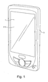
- Fig. 1 is a perspective view showing a capacitive touch panel of the invention assembled in a shell of an electronic device
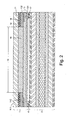
- Fig. 2 is a sectional view of the capacitive touch panel of Fig. 1 according to one embodiment of the invention
- Fig. 3 is a sectional view of the capacitive touch panel according to a transformation of Fig. 2 ;
- Fig. 4 is a sectional view of the capacitive touch panel of the Fig. 1 according to another embodiment of the invention.
- Fig. 5 is a sectional view of the capacitive touch panel according to a transformation of Fig. 4 ;
- Fig. 6 is a sectional view of a touch display panel of the applicant according to a prior not prepublished embodiment.
- Fig. 1 is a perspective view showing a capacitive touch panel 1 of the invention assembled in a shell 3 of an electronic device.
- Fig. 2 is a sectional view showing the capacitive touch panel 1 assembled on an upper surface of a display plane 2 according to one embodiment of the invention.
- the capacitive touch panel 1 includes a lens 11, a mask layer 12 and a sensing circuit layer 13.
- the lens 11 may be made of glass, rubber or ebonite, and the lens 11 includes an upper surface 111 for touching and a lower surface 112 for bonding.
- the mask layer 12 is provided on the periphery of the lower surface 112, and the mask layer 12 may be a block matrix or other opaque coating layer.
- the sensing circuit layer 13 is provided under the lens 11, and the mask layer 12 covers the periphery of the sensing circuit layer 13 so that a sensing region 14 is exposed.
- a smooth layer 15 made of transparent organic or inorganic material is provided to be sandwiched in between the lens 11 and the sensing circuit layer 13.
- the touch range of the sensing region 14 includes the area of the lens 11 that is formed on the smooth layer but not formed on the mask layer 12.
- the sensing circuit layer 13 is provided on a lower surface of the mask layer 12 and a lower surface of the smooth layer 15.
- the smooth layer 15 can smooth the lower surface of the mask layer 12 so that the yield rate can be enhanced.
- a shielding layer 16 is provided between the 11 and the mask layer 12 to prevent noise signals.
- the width of the shielding layer 16 may be the same as that of the mask layer 12.
- the sensing circuit layer 13 may be formed by coating, exposing, developing and etching.
- the sensing circuit layer 13 includes a single conductive film 131.
- the sensing circuit layer 13 also includes a metal trace arranged on the periphery of the single conductive film 131.
- the metal trace (metal trace 132 as shown in Fig. 2 ) can be arranged on the periphery of the upper surface of the single conductive film 131.
- the metal trace (metal trace 133 as shown in Fig. 3 ) also can be arranged on the periphery of the lower surface of the single conductive film 131.
- the mask layer 12 covers the metal trace 132, 133 to prevent the metal trace 132, 133 from being exposed on the lens 11. Thus, the appearance of the lens 11 is prettified.
- the single conductive film 131 is made of transparent conductive material (such as ITO).
- An over coat 17 (as shown in Fig. 2 ) is coated on the lower surface of the sensing circuit layer 13.
- An adhesive layer 4 is provided between the periphery of the over coat 17 and the periphery of the display panel 2. As shown in Fig. 3 , the over coat 17 can be omitted, and the adhesive layer 4 is directly bonded to an upper polarizing plate 21 of the display panel 2.
- the display panel 2 can display images and letters through the lens 11, the single conductive film 131 and the smooth layer 15.
- the single conductive film 131 in the sensing region will output a capacitive sensing signal corresponding to the touched position because of a capacitive effect produced by a user finger touch sensing of the upper surface 111.
- the capacitive sensing signal is transmitted to a processor for detecting the touched position (not shown) through the metal trace 132 (shown in Fig. 2 ), the metal trace 133 (shown in Fig. 3 ).
- the sensing circuit layer 13 is provided on the inner side of the lens 11 to form a capacitive touch circuit of a touch panel, so the capacitive touch panel 1 has a touch sensing ability.
- a glass substrate conventionally arranged between a lens and a display panel can be omitted, and the capacitive touch panel 1 of the invention can be directly arranged on the upper surface of the display panel 2. Therefore, the glass substrate used in conventional touch panel can be omitted, and the conventional panel bonding process can be simplified. The cost and time for producing the touch panel can be reduced and the touch panel can be also form of slim type design.
- Fig. 4 is a sectional view showing the capacitive touch panel 1a assembled on an upper surface of a display device 2a according to another embodiment of the invention.
- the capacitive touch panel 1a includes a lens 11a, a mask layer 12a, a first sensing circuit layer 13a, a transparent insulation layer 18a and a second sensing circuit layer 19a.
- the lens 11 a is made of glass, rubber or ebonite, and includes an upper surface 111 a for touching and a lower surface 112a for bonding.
- the mask layer 12a is provided on the periphery of the lower surface 112a, and the mask layer 12a may be a black matrix or other opaque coating layer.
- the first sensing circuit layer 13a is provided under the lens 11a, and the mask layer 12 covers the periphery of the first sensing circuit layer 13a so that a sensing region 14a is exposed.
- the transparent insulation layer 18a is provided to at least cover the lower surface of the first sensing circuit layer 13a of the sensing region 14a.
- the second sensing circuit layer 19a is provided on the lower surface of the transparent insulation layer 18a.
- first sensing circuit layer 13a and the second sensing circuit layer 19a would effect the distribution area of transparent insulation layer 18a.
- the insulation layer 18a would be fully distributed between the two sensing layers; but when the two sensing layers are in the form of non-parallel structure and existing an intersection area between them. In these cases, the insulation layer 18a is used to electrically insulate the first sensing circuit layer 13a and the second sensing circuit layer 19a. But in the later structure, the insulation layer 18a would be fully distributed between the two sensing layers or just only be distributed on that intersection area.
- the touch range of the sensing region 14a includes areas that are not covered by the mask layer 12a.
- a smooth layer 15a (as shown in Fig. 4 ) made of transparent organic or inorganic material is provided in the sensing region 14a to fill up the space between the lens 11a and the first sensing circuit layer 13a.
- the first sensing circuit layer 13a is provided on the lower surface of the mask layer 12a and the lower surface of the smooth layer 15a.
- a shielding layer 16a is provided between the lens 11 a and the mask layer 12a to prevent noise signals. The width of the shielding layer 16a can be the same as that of the mask layer 12a.
- the first sensing circuit layer 13a includes a first (upper) conductive film 134a.
- the first sensing circuit layer 13a also includes a metal trace arranged on the periphery of the upper conductive film 134a.
- the metal trace metal trace 132a as shown in Fig. 4
- the metal trace metal trace 133a as shown in Fig. 5
- the mask layer 12a covers the metal trace 132a, 133a to prevent the metal trace 132a, 133a from being exposed on the lens 11a.
- the appearance of the lens 11a is prettified.
- the second sensing circuit layer 19a includes a second (lower) conductive film 134b. Besides the lower conductive film 134b, the second sensing circuit layer 19a also includes a metal trace arranged on the periphery of the lower conductive film 134b.
- the metal trace (metal trace 132b as shown in Fig. 4 ) can be arranged on the periphery of the upper surface of the lower conductive film 134b.
- the metal trace (metal trace 133b as shown in Fig. 5 ) also can be arranged on the periphery of the lower surface of the lower conductive film 134b.
- the mask layer 12a covers the metal trace 132b, 133b to prevent the metal trace 132b, 133b from being exposed on the lens 11a. Thus, the appearance of the lens 11a is prettified.
- an over coat 17a (as shown in Fig. 4 ) is coated on the lower surface of the second sensing circuit layer 19a.
- An adhesive layer 4a is provided between the periphery of the over coat 17a and the periphery of the display panel 2a. As shown in Fig. 5 , the over coat 17a can be omitted, and the adhesive layer 4a is directly bonded to an upper polarizing plate 21a of the display panel 2a.
- the upper conductive film 134a and the lower conductive film 134b in the sensing region 14a will respectively output a capacitive sensing signal corresponding to the touched position because of a capacitive effect produced by a user finger touch sensing of the upper surface 111a.
- the capacitive sensing signals are transmitted to a processor (not shown) through the corresponding metal traces for detecting the touched position.
- the capacitive sensing signal also can be transmitted to the processor through corresponding conductive films for detecting the touched position.
Landscapes
- Engineering & Computer Science (AREA)
- Theoretical Computer Science (AREA)
- General Engineering & Computer Science (AREA)
- Physics & Mathematics (AREA)
- General Physics & Mathematics (AREA)
- Human Computer Interaction (AREA)
- Computer Hardware Design (AREA)
- Nonlinear Science (AREA)
- Mathematical Physics (AREA)
- Chemical & Material Sciences (AREA)
- Crystallography & Structural Chemistry (AREA)
- Optics & Photonics (AREA)
- Position Input By Displaying (AREA)
Claims (15)
- Kapazitives Berührungsbedienfeld (1, 1a), umfassend:eine Linse (11, 11a), die eine obere Oberfläche (111, 111a) zum Berühren und eine untere Oberfläche (112, 112a) zum Verbinden aufweist;eine unter der Linse (11, 11a) ausgebildete Sensierschaltungsschicht (13, 13a); und eine an einer Peripherie der unteren Oberfläche (112, 112a) der Linse (11, 11a) ausgebildete Maskierungsschicht (12, 12a);die Maskierungsschicht (12, 12a) bedeckt eine Peripherie der Sensierschaltungsschicht (13, 13a) um eine Sensierregion (14, 14a) darzubieten;die Sensierschaltungsschicht (13, 13a) weist eine transparente, leitfähige Schicht (131, 134a) und eine auf einer Peripherie der transparenten, leitfähigen Schicht (131, 134a) angeordnete Metallleiterbahn (133, 132a) auf;die Maskierungsschicht (12, 12a) bedeckt die Metallleiterbahn (133, 132a) und/oder ist auf einer Metallleiterbahn (132, 132a) angeordnet;die Sensierschaltungsschicht (13, 13a) ist zur Ausgabe eines Sensiersignals für einen durch eine Berührungssensierung der oberen Oberfläche (111, 111a) der Linse (11, 11a) erzeugten kapazitiven Effekt in der Lage, das über die Metallleiterbahn (132, 132a) zu einem Prozessor zur Erkennung der berührten Position übertragen wird, und das kapazitive Berührungsbedienfeld (1, 1a) ist geeignet, um auf der oberen Oberfläche eines Anzeigefelds (2, 2a) angeordnet zu werden, wobei das kapazitive Berührungsbedienfeld weiterhin eine zwischen der Linse (11, 11a) und der Sensierschaltungsschicht (13, 13a) angeordnete Ebnungsschicht (15, 15a) zum Auffüllen des Raumes zwischen der Linse (11, 11a) und der Sensierschaltungsschicht (13, 13a) aufweist, wobei ein Berührungsbereich der Sensierregion (14, 14a) einen Bereich der Linse (11, 11a) aufweist, der mit der Ebnungsschicht (15, 15a) kontaktiert ist, und/oder die Sensierschaltungsschicht (13, 13a) auf einer unteren Oberfläche der Maskierungsschicht (12, 12a) und einer unteren Oberfläche der Ebungsschicht (15, 15a) angeordnet ist.
- Kapazitives Berührungsbedienfeld nach Anspruch 1, dadurch gekennzeichnet, dass
die Ebnungsschicht (15, 15a) aus transparentem organischem oder anorganischem Material gefertigt ist. - Kapazitives Berührungsbedienfeld nach Anspruch 1, dadurch gekennzeichnet, dass
die Linse (11, 11a) aus Glas, Gummi oder Ebonit gefertigt ist. - Kapazitives Berührungsbedienfeld nach Anspruch 1, dadurch gekennzeichnet, dass
die Maskierungsschicht (12, 12a) aus opakem Beschichtungsmaterial gefertigt ist. - Kapazitives Berührungsbedienfeld nach Anspruch 1, weiterhin aufweisend
eine zwischen der Linse (11, 11a) und der Maskierungsschicht (12, 12a) vorgesehene Abschirmschicht (16, 16a) zur Verhinderung von Störsignalen. - Kapazitives Berührungsbedienfeld nach Anspruch 1, dadurch gekennzeichnet, dass
die Metallleiterbahn (133, 132a) auf einer Peripherie einer oberen Oberfläche oder einer unteren Oberfläche der leitfähigen Schicht (131, 134a) ausgebildet ist. - Kapazitives Berührungsbedienfeld nach Anspruch 1, weiterhin aufweisend
eine auf einer unteren Oberfläche der Sensierschaltungsschicht (13, 19a) vorgesehene Bedeckung (17, 17a) und
eine unter der Bedeckung (17, 17a) zum Verbinden mit dem Anzeigefeld (2, 2a) vorgesehene Adhäsionsschicht (4, 4a). - Kapazitives Berührungsbedienfeld nach Anspruch 1, weiterhin aufweisend
eine auf einer unteren Oberfläche der Sensierschaltungsschicht (13, 19a) zum Verbinden mit einer polarisierenden Scheibe des Anzeigefelds (2, 2a) vorgesehene Adhäsionsschicht (4, 4a). - Kapazitives Berührungsbedienfeld nach Anspruch 1, wobei
die Sensierschaltungsschicht eine erste Sensierschaltungsschicht (13a) aufweist, die zur Ausgabe eines ersten Sensiersignals für einen durch Berührungssensierung der oberen Oberfläche (111a) der Linse (11a) erzeugten kapazitiven Effekt geeignet ist;
eine zweite Sensierschaltungsschicht (19a) aufweist, die zur Ausgabe eines zweiten Messsignals für einen durch die Berührungssensierung erzeugten kapazitiven Effekt geeignet ist; und
eine Isolierungsschicht (18a) aufweist, die zumindest eine untere Oberfläche der ersten Sensierschaltungsschicht (13a) bedeckt, wobei die Ebnungsschicht (15a) zum Auffüllen des Raumes zwischen der Linse (11a) und der ersten Sensierschaltungsschicht (13a) zwischen der Linse (11a) und der ersten Sensierschaltungsschicht (13a) angeordnet ist, wobei ferner ein Berührungsbereich der Sensierregion (14a) einen Bereich der Linse (11a) aufweist, der mit der Ebnungsschicht (15a) kontaktiert ist, und dass die erste Sensierschaltungsschicht (13a) auf einer unteren Oberfläche der Maskierungsschicht (12a) und einer unteren Oberfläche der Ebnungsschicht (15a) angeordnet ist. - Kapazitives Berührungsbedienfeld nach Anspruch 9, dadurch gekennzeichnet, dass
die Isolierungsschicht (18a) aus einem transparenten Isoliermaterial gefertigt ist. - Kapazitives Berührungsbedienfeld nach Anspruch 9, dadurch gekennzeichnet, dass
die erste Sensierschaltungsschicht (13a) unter der Linse (11a) ausgebildet ist, dass die Maskierungsschicht (12a) eine Peripherie der ersten Sensierschaltungsschicht (13a) bedeckt, um die Sensierregion (14a) darzubieten, die zweite Sensierschaltungsschicht (19a) auf einer unteren Oberfläche der Isolierungsschicht (18a) ausgebildet ist, das zweite Sensiersignal durch Berührungserkennung der Sensierregion (14a) erzeugt wird und/oder die zweite Sensierschaltungsschicht (19a) auf einer unteren Oberfläche der Isolierungsschicht (18a) vorgesehen ist. - Kapazitives Berührungsbedienfeld nach Anspruch 9 oder 11, weiterhin aufweisend
eine Abschirmschicht (16a) zwischen der Linse (11a) und der Maskierungsschicht (12a) zur Verhinderung von Störsignalen oder wobei die erste Sensierschaltungsschicht (13a) eine erste leitfähige Schicht (134a) und die zweite Sensierschaltungsschicht (19) eine zweite leitfähige Schicht (134b) aufweist. - Kapazitives Berührungsbedienfeld nach Anspruch 9 oder 11, dadurch gekennzeichnet, dass
die transparente leitfähige Schicht eine erste leitfähige Schicht (134a) und eine zweite leitfähige Schicht (134b) aufweist und die Metallleiterbahn eine erste Metallleiterbahn (132a, 133a) und eine zweite Metallleiterbahn (132b, 133b) aufweist, wobei die erste Sensierschaltungsschicht (13a) die erste leitfähige Schicht (134b) und die auf einer Peripherie oder einer oberen Oberfläche oder einer unteren Oberfläche der ersten leitfähigen Schicht (134a) ausgebildete erste Metallleiterbahn (132a, 133a) aufweist und/oder die zweite Sensierschaltungsschicht (19a) die zweite leitfähige Schicht (134b) und die auf einer Peripherie oder einer oberen Oberfläche oder einer unteren Oberfläche der zweiten leitfähigen Schicht (134b) ausgebildete zweite Metallleiterbahn (132b, 133b) aufweist, wobei die Maskierungsschicht (12a) die Peripherie der ersten Sensierschaltungsschicht bedeckt (13a), die Metallleiterbahn (132a) bedeckt und/oder auf der Metallleiterbahn (132a) angeordnet ist. - Kapazitives Berührungsbedienfeld nach Anspruch 9 oder 11, weiterhin aufweisend
eine auf einer unteren Oberfläche der zweiten Sensierschaltungsschicht (19a) vorgesehene Bedeckung (17a) und eine unter der Bedeckung (17a) zum Verbinden mit dem Anzeigefeld (2a) vorgesehene Adhäsionsschicht (4a) oder eine auf einer unteren Oberfläche der zweiten Sensierschaltungsschicht (19a) zum Verbinden mit einer polarisierenden Scheibe des Anzeigefelds (2a) vorgesehene Adhäsionsschicht (2a). - Anordnung, die ein kapazitives Berührungsbedienfeld (1, 1a) nach einem der vorhergehenden Ansprüche und ein Anzeigefeld (2, 2a) aufweist, dadurch gekennzeichnet, dass das kapazitive Berührungsbedienfeld (1, 1a) auf einer oberen Oberfläche des Anzeigefelds (2, 2a) montiert ist.
Priority Applications (3)
| Application Number | Priority Date | Filing Date | Title |
|---|---|---|---|
| EP14162989.9A EP2752743B1 (de) | 2008-02-18 | 2009-02-17 | Kapazitiver Berührungsbildschirm |
| DE09002202T DE09002202T1 (de) | 2008-02-18 | 2009-02-17 | Kapazitiver Berührungsbildschirm |
| EP09002202.1A EP2090967B1 (de) | 2008-02-18 | 2009-02-17 | Kapazitiver Berührungsbildschirm |
Applications Claiming Priority (1)
| Application Number | Priority Date | Filing Date | Title |
|---|---|---|---|
| TW097202841U TWM348999U (en) | 2008-02-18 | 2008-02-18 | Capacitive touch panel |
Publications (2)
| Publication Number | Publication Date |
|---|---|
| EP2090966A1 EP2090966A1 (de) | 2009-08-19 |
| EP2090966B1 true EP2090966B1 (de) | 2012-12-19 |
Family
ID=39865244
Family Applications (3)
| Application Number | Title | Priority Date | Filing Date |
|---|---|---|---|
| EP08155297A Active EP2090966B1 (de) | 2008-02-18 | 2008-04-28 | Kapazitiver Berührungsbildschirm |
| EP09002202.1A Active EP2090967B1 (de) | 2008-02-18 | 2009-02-17 | Kapazitiver Berührungsbildschirm |
| EP14162989.9A Active EP2752743B1 (de) | 2008-02-18 | 2009-02-17 | Kapazitiver Berührungsbildschirm |
Family Applications After (2)
| Application Number | Title | Priority Date | Filing Date |
|---|---|---|---|
| EP09002202.1A Active EP2090967B1 (de) | 2008-02-18 | 2009-02-17 | Kapazitiver Berührungsbildschirm |
| EP14162989.9A Active EP2752743B1 (de) | 2008-02-18 | 2009-02-17 | Kapazitiver Berührungsbildschirm |
Country Status (6)
| Country | Link |
|---|---|
| US (4) | US8665226B2 (de) |
| EP (3) | EP2090966B1 (de) |
| JP (3) | JP5199913B2 (de) |
| KR (1) | KR101141253B1 (de) |
| DE (2) | DE09002202T1 (de) |
| TW (1) | TWM348999U (de) |
Cited By (1)
| Publication number | Priority date | Publication date | Assignee | Title |
|---|---|---|---|---|
| EP3508962A1 (de) * | 2010-11-09 | 2019-07-10 | TPK Touch Solutions Inc. | Berührungsbildschirmstapel |
Families Citing this family (75)
| Publication number | Priority date | Publication date | Assignee | Title |
|---|---|---|---|---|
| TWI374379B (en) | 2007-12-24 | 2012-10-11 | Wintek Corp | Transparent capacitive touch panel and manufacturing method thereof |
| TWM348999U (en) * | 2008-02-18 | 2009-01-11 | Tpk Touch Solutions Inc | Capacitive touch panel |
| KR100894710B1 (ko) * | 2008-06-27 | 2009-04-24 | (주) 월드비젼 | 윈도우 일체형 터치스크린 및 이의 제조방법 |
| KR20100053349A (ko) * | 2008-11-12 | 2010-05-20 | 엘지전자 주식회사 | 터치 모듈, 그 터치 모듈의 제조 방법 및 그 터치 모듈을 갖는 휴대 단말기 |
| TWI412817B (zh) * | 2009-06-02 | 2013-10-21 | Wintek Corp | 觸控顯示裝置 |
| TWI451313B (zh) * | 2009-06-26 | 2014-09-01 | Ritfast Corp | 電容式觸控面板 |
| TW201120712A (en) * | 2009-12-09 | 2011-06-16 | J Touch Corp | Capacitive touch device structure. |
| US9019233B2 (en) | 2010-01-26 | 2015-04-28 | Tpk Touch Solutions Inc. | Projected capacitive touch panel and method of manufacturing the same |
| TW201102698A (en) | 2010-01-26 | 2011-01-16 | Mastouch Optoelectronics Technologies Co Ltd | Single-layer projected capacitive touch panel and fabricating method thereof |
| JP5606093B2 (ja) * | 2010-02-17 | 2014-10-15 | アルプス電気株式会社 | 入力装置 |
| KR101113467B1 (ko) | 2010-04-01 | 2012-02-29 | 삼성모바일디스플레이주식회사 | 터치 스크린 패널 |
| KR101113471B1 (ko) * | 2010-04-01 | 2012-02-29 | 삼성모바일디스플레이주식회사 | 터치 스크린 패널 |
| TW201102702A (en) | 2010-05-11 | 2011-01-16 | Mastouch Optoelectronics Technologies Co Ltd | Capacitive touch panel |
| US8947399B2 (en) | 2010-05-11 | 2015-02-03 | Tpk Touch Solutions Inc. | Dual-substrate capacitive touch panel |
| US9471826B2 (en) * | 2010-05-21 | 2016-10-18 | Blackberry Limited | Determining fingerprint scanning mode from capacitive touch sensor proximate to lens |
| TWI472834B (zh) * | 2010-05-27 | 2015-02-11 | 宸鴻科技(廈門)有限公司 | A stacked structure for enhancing the bonding strength of a touch panel and a method of manufacturing the same |
| TW201205383A (en) * | 2010-05-31 | 2012-02-01 | Wintek Corp | Touch-sensitive device |
| TW201145125A (en) * | 2010-06-03 | 2011-12-16 | J Touch Corp | Touch panel manufacturing method and structure thereof |
| TWI456443B (zh) * | 2010-06-07 | 2014-10-11 | Wintek Corp | 觸控裝置及觸控顯示裝置 |
| CN102279658A (zh) * | 2010-06-11 | 2011-12-14 | 介面光电股份有限公司 | 触控面板制造方法及其结构 |
| US9652088B2 (en) * | 2010-07-30 | 2017-05-16 | Apple Inc. | Fabrication of touch sensor panel using laser ablation |
| KR101438484B1 (ko) * | 2010-10-07 | 2014-11-04 | 주식회사 에스에스디 | 블랭크 터치 제조방법 |
| CN102446040B (zh) * | 2010-10-11 | 2015-02-18 | 联建(中国)科技有限公司 | 电容式触控面板 |
| KR101455014B1 (ko) * | 2010-11-02 | 2014-10-27 | 쇼와 덴코 가부시키가이샤 | 정전 용량 터치 패널용 입력 디바이스, 입력 방법 및 집합체 |
| US9563315B2 (en) * | 2010-11-09 | 2017-02-07 | Tpk Touch Solutions Inc. | Capacitive touch panel and method for producing the same |
| EP2638453A4 (de) | 2010-11-09 | 2015-11-25 | Tpk Touch Solutions Inc | Berührungsbildschirmvorrichtung |
| KR101793073B1 (ko) * | 2010-12-06 | 2017-11-03 | 삼성디스플레이 주식회사 | 터치 스크린 패널 |
| KR101773514B1 (ko) | 2010-12-15 | 2017-09-01 | 삼성디스플레이 주식회사 | 터치스크린 일체형 평판표시장치 |
| KR101722229B1 (ko) | 2010-12-15 | 2017-04-03 | 삼성디스플레이 주식회사 | 터치 스크린 일체형 평판 표시 장치 |
| KR101181342B1 (ko) * | 2011-02-16 | 2012-09-11 | 에쓰이에이치에프코리아 (주) | 터치스크린 |
| CN102654798A (zh) * | 2011-03-03 | 2012-09-05 | 宸鸿光电科技股份有限公司 | 触控感测装置及其制造方法 |
| CN102681709B (zh) * | 2011-03-17 | 2016-01-27 | 宸鸿光电科技股份有限公司 | 触控显示设备及其制造方法 |
| CN102681712B (zh) | 2011-03-18 | 2016-08-24 | 宸鸿科技(厦门)有限公司 | 触控装置及其制造方法 |
| JP5066272B2 (ja) * | 2011-03-29 | 2012-11-07 | アルプス電気株式会社 | 入力装置及びその製造方法 |
| JP5244938B2 (ja) | 2011-03-29 | 2013-07-24 | アルプス電気株式会社 | 入力装置及びその製造方法 |
| JP5097840B2 (ja) | 2011-03-29 | 2012-12-12 | アルプス電気株式会社 | 入力装置及びその製造方法 |
| CN102736760B (zh) * | 2011-04-11 | 2015-12-02 | 富创得科技股份有限公司 | 触控面板单面结构及其制作方法 |
| KR101330757B1 (ko) * | 2011-07-28 | 2013-11-18 | 엘지이노텍 주식회사 | 터치윈도우 및 이를 포함하는 액정표시장치 |
| CN102929454A (zh) * | 2011-08-12 | 2013-02-13 | 宸鸿科技(厦门)有限公司 | 电容式触控面板及降低其金属导体可见度的方法 |
| JP5825055B2 (ja) * | 2011-09-29 | 2015-12-02 | 王子ホールディングス株式会社 | 反射防止体、静電容量式タッチパネルおよび静電容量式タッチパネル付き表示装置 |
| TWI471774B (zh) * | 2011-09-30 | 2015-02-01 | Wintek Corp | 觸控裝置及觸控顯示裝置 |
| KR101501907B1 (ko) | 2011-11-07 | 2015-03-12 | 오지 홀딩스 가부시키가이샤 | 정전 용량식 터치 패널이 형성된 표시 장치, 정전 용량식 터치 패널 |
| CN103176641A (zh) * | 2011-12-25 | 2013-06-26 | 宸鸿科技(厦门)有限公司 | 触控面板及其制作方法 |
| JP5234868B1 (ja) * | 2011-12-28 | 2013-07-10 | 日本写真印刷株式会社 | 光学機能付き静電容量方式タッチセンサー |
| CN104137038B (zh) * | 2012-01-09 | 2017-08-25 | 谷歌公司 | 具有手指鉴别的智能触摸屏键盘 |
| CN114089600B (zh) | 2012-03-15 | 2024-12-03 | 富士胶片株式会社 | 静电电容型输入装置及其制造方法、图像显示装置 |
| JP5949029B2 (ja) * | 2012-03-26 | 2016-07-06 | 大日本印刷株式会社 | 表示装置用前面保護板、及び表示装置 |
| CN104246611B (zh) | 2012-03-30 | 2018-12-04 | 富士胶片株式会社 | 黑色树脂膜、静电电容型输入装置及它们的制造方法及具备其的图像显示装置 |
| FR2990020B1 (fr) * | 2012-04-25 | 2014-05-16 | Fogale Nanotech | Dispositif de detection capacitive avec arrangement de pistes de liaison, et procede mettant en oeuvre un tel dispositif. |
| JP5926128B2 (ja) * | 2012-06-19 | 2016-05-25 | 富士フイルム株式会社 | 光硬化性樹脂層を有する積層体の製造方法並びに静電容量型入力装置とその製造方法及びそれを備えた画像表示装置 |
| JP5955787B2 (ja) | 2012-06-20 | 2016-07-20 | 富士フイルム株式会社 | 転写フィルム、静電容量型入力装置の製造方法および静電容量型入力装置、並びに、これを備えた画像表示装置 |
| CN102778987A (zh) * | 2012-06-29 | 2012-11-14 | 华为终端有限公司 | 投射式电容触摸屏及其制备方法 |
| CN103576949B (zh) * | 2012-07-24 | 2017-02-15 | 宸鸿科技(厦门)有限公司 | 触控面板及其制造方法 |
| US9244558B2 (en) * | 2012-08-16 | 2016-01-26 | Eastman Kodak Company | Pixel-aligned electrode device |
| CN103631409B (zh) * | 2012-08-21 | 2017-01-11 | 宸鸿科技(厦门)有限公司 | 触控装置及其制造方法 |
| TWI448942B (zh) * | 2012-08-28 | 2014-08-11 | 恆顥科技股份有限公司 | 觸控面板 |
| US9323365B2 (en) * | 2012-10-29 | 2016-04-26 | Google Inc. | Masking an outer perimeter of a touch screen |
| WO2014115646A1 (ja) * | 2013-01-25 | 2014-07-31 | 富士フイルム株式会社 | 透明樹脂膜、転写フィルム、導電膜積層体、静電容量型入力装置および画像表示装置 |
| TWI492163B (zh) * | 2013-02-20 | 2015-07-11 | Smartdisplayer Technology Co Ltd | Electronic card and its capacitive touch sensing method |
| WO2014175312A1 (ja) * | 2013-04-26 | 2014-10-30 | 富士フイルム株式会社 | 転写材料、転写層付き基材及びタッチパネル、それらの製造方法、並びに情報表示装置 |
| JP6221427B2 (ja) * | 2013-07-05 | 2017-11-01 | 大日本印刷株式会社 | 表示装置用前面保護板及び表示装置 |
| US20150022729A1 (en) * | 2013-07-22 | 2015-01-22 | Teh-Zheng Lin | Layered assembly of touch panel |
| JP6286912B2 (ja) * | 2013-07-26 | 2018-03-07 | 大日本印刷株式会社 | 表示装置用前面保護板及び表示装置 |
| TWI488088B (zh) * | 2013-08-08 | 2015-06-11 | Univ Nat Taiwan | 具觸控功能的電子裝置 |
| JP5848736B2 (ja) | 2013-09-06 | 2016-01-27 | デクセリアルズ株式会社 | 静電容量型タッチパネル |
| CN104635969A (zh) * | 2013-11-14 | 2015-05-20 | 索尼公司 | 触摸屏、电子设备以及防止触摸屏漏光的方法 |
| US9921672B2 (en) * | 2014-01-28 | 2018-03-20 | Mediatek Inc. | Electronic devices, near field communication methods and near field communication systems |
| TWI549027B (zh) * | 2014-04-22 | 2016-09-11 | 群創光電股份有限公司 | 觸控面板及觸控顯示裝置 |
| JP6416668B2 (ja) * | 2014-08-20 | 2018-10-31 | 株式会社ジャパンディスプレイ | 表示装置 |
| JP2016051477A (ja) * | 2014-08-29 | 2016-04-11 | デクセリアルズ株式会社 | タッチパネルおよびタッチパネル付き表示装置 |
| CN104765518B (zh) * | 2015-04-20 | 2017-11-07 | 合肥鑫晟光电科技有限公司 | 一种触摸基板及其制造方法、显示装置 |
| JP2017021346A (ja) | 2015-07-10 | 2017-01-26 | Jsr株式会社 | 硬化性組成物、硬化膜、ベゼル及び表示装置 |
| JP6411389B2 (ja) * | 2016-02-04 | 2018-10-24 | 大日本印刷株式会社 | 表示装置用前面保護板、及び表示装置 |
| JP6323594B2 (ja) * | 2017-04-26 | 2018-05-16 | 大日本印刷株式会社 | 表示装置用前面保護板及び表示装置 |
| US20220320475A1 (en) * | 2019-08-19 | 2022-10-06 | Boe Technology Group Co., Ltd. | Flexible display apparatus and fabrication method thereof |
Citations (7)
| Publication number | Priority date | Publication date | Assignee | Title |
|---|---|---|---|---|
| US20030234770A1 (en) * | 2002-06-25 | 2003-12-25 | Mackey Bob Lee | Capacitive sensing device |
| US20040238835A1 (en) * | 2003-03-12 | 2004-12-02 | Asulab S. A. | Substrate with transparent electrodes and devices incorporating it |
| WO2004114265A2 (en) * | 2003-06-20 | 2004-12-29 | Cirque Corporation | Single-layer touchpad and methods of use |
| US20050126831A1 (en) * | 2003-12-15 | 2005-06-16 | Richter Paul J. | Wiring harness and touch sensor incorporating same |
| WO2005114369A2 (en) * | 2004-05-06 | 2005-12-01 | Apple Computer, Inc. | Multipoint touchscreen |
| US20060114374A1 (en) * | 2004-11-30 | 2006-06-01 | Yasuo Segawa | Liquid crystal display device |
| US20060146033A1 (en) * | 2005-01-04 | 2006-07-06 | Toppoly Optoelectronics Corp. | Display devices and methods forming the same |
Family Cites Families (78)
| Publication number | Priority date | Publication date | Assignee | Title |
|---|---|---|---|---|
| JPS6075927A (ja) | 1983-09-30 | 1985-04-30 | Fujitsu Ltd | 座標入力装置 |
| US5457289A (en) * | 1994-03-16 | 1995-10-10 | Microtouch Systems, Inc. | Frontally shielded capacitive touch sensor system |
| JPH09258893A (ja) | 1996-03-25 | 1997-10-03 | Toshiba Corp | 座標入力装置、およびこれを備えた入力表示装置 |
| KR100293435B1 (ko) * | 1997-10-31 | 2001-08-07 | 구본준, 론 위라하디락사 | 위치검출액정디스플레이장치(pslcd)및이의제조방법 |
| EP1046946B1 (de) * | 1998-01-09 | 2008-05-28 | Nissha Printing Co., Ltd. | Flüssigkristallanzeige mit berührungseingabe und herstellungsverfahren |
| US6259491B1 (en) * | 1998-02-06 | 2001-07-10 | Motorola, Inc. | Double sided laminated liquid crystal display touchscreen and method of making same for use in a wireless communication device |
| US6933991B2 (en) * | 1999-01-22 | 2005-08-23 | White Electronic Designs Corp. | Super bright low reflectance liquid crystal display |
| JP2001282454A (ja) * | 2000-03-31 | 2001-10-12 | Nissha Printing Co Ltd | 周縁部に遮光性を有するタッチパネル |
| US6876355B1 (en) * | 2000-05-18 | 2005-04-05 | Lg. Philips Lcd Co., Ltd. | Touch screen structure to prevent image distortion |
| JP2002366302A (ja) | 2001-06-05 | 2002-12-20 | Mitsubishi Electric Corp | タッチパネル付き設定表示装置 |
| JP2003173238A (ja) | 2001-12-05 | 2003-06-20 | Sharp Corp | タッチセンサおよびタッチセンサ付き表示装置 |
| CN1301510C (zh) | 2001-10-05 | 2007-02-21 | 普利司通股份有限公司 | 透明导电性薄膜、其制造方法以及触摸面板 |
| US7126589B2 (en) * | 2002-05-29 | 2006-10-24 | Au Optronics Corporation | Touch control panel |
| EP1387246A1 (de) * | 2002-07-30 | 2004-02-04 | Motorola, Inc. | Benutzerschnittstelle und Verfahren zur Anzeige von Informationen auf mehreren Anzeigevorrichtungen |
| US6879319B2 (en) * | 2002-10-25 | 2005-04-12 | Eastman Kodak Company | Integrated OLED display and touch screen |
| US6970160B2 (en) | 2002-12-19 | 2005-11-29 | 3M Innovative Properties Company | Lattice touch-sensing system |
| US20050030048A1 (en) * | 2003-08-05 | 2005-02-10 | Bolender Robert J. | Capacitive sensing device for use in a keypad assembly |
| US8068186B2 (en) * | 2003-10-15 | 2011-11-29 | 3M Innovative Properties Company | Patterned conductor touch screen having improved optics |
| KR20070017296A (ko) | 2003-10-15 | 2007-02-09 | 쓰리엠 이노베이티브 프로퍼티즈 컴파니 | 개선된 광학 특성을 갖는 패턴화된 도체 터치 스크린 |
| US20050110766A1 (en) * | 2003-11-24 | 2005-05-26 | Elo Touchsystems, Inc. | Touch sensor with conductive polymer switches |
| JP4545424B2 (ja) * | 2003-12-11 | 2010-09-15 | アルプス電気株式会社 | 座標入力装置及びそれを備えた画像表示装置と電子機器 |
| CA2551595C (en) | 2003-12-26 | 2011-02-08 | Nissha Printing Co., Ltd. | Electronic device with protection panel, protection panel, and method offabricating protection panels |
| US20050260338A1 (en) * | 2004-05-19 | 2005-11-24 | Trendon Touch Technology Corp. | Method of manufacturing circuit layout on touch panel by utilizing metal plating technology |
| JP4435622B2 (ja) * | 2004-05-25 | 2010-03-24 | アルプス電気株式会社 | 静電容量式の検出装置 |
| US7358741B2 (en) * | 2004-05-25 | 2008-04-15 | Alps Electric Co., Ltd | Electrostatic detection apparatus and method, and coordinate detection program |
| US7164293B2 (en) * | 2004-07-29 | 2007-01-16 | Freescale Semiconductor, Inc. | Dynamic latch having integral logic function and method therefor |
| US20060227114A1 (en) * | 2005-03-30 | 2006-10-12 | Geaghan Bernard O | Touch location determination with error correction for sensor movement |
| US8354143B2 (en) * | 2005-05-26 | 2013-01-15 | Tpk Touch Solutions Inc. | Capacitive touch screen and method of making same |
| JP4610416B2 (ja) * | 2005-06-10 | 2011-01-12 | 日本写真印刷株式会社 | 静電容量型タッチパネル |
| EP1746485A2 (de) * | 2005-07-21 | 2007-01-24 | TPO Displays Corp. | Verfahren zur Integration eines Digitalisiereingabegeräts in eine Anzeige |
| JP2007034644A (ja) * | 2005-07-27 | 2007-02-08 | Central Glass Co Ltd | 可視光透過型平面コイル素子 |
| US7486280B2 (en) * | 2005-08-04 | 2009-02-03 | Uniplas Enterprises Pte, Ltd. | Contoured capacitive touch control panel |
| US7839392B2 (en) * | 2005-08-05 | 2010-11-23 | Samsung Electronics Co., Ltd. | Sensing circuit and display device having the same |
| JP4797504B2 (ja) * | 2005-08-09 | 2011-10-19 | ソニー株式会社 | 入力装置及びこれを用いた表示装置 |
| KR101152136B1 (ko) * | 2005-10-26 | 2012-06-15 | 삼성전자주식회사 | 접촉 감지 기능이 있는 표시 장치 |
| JP4539533B2 (ja) * | 2005-11-01 | 2010-09-08 | エプソンイメージングデバイス株式会社 | 電気光学装置及び電子機器 |
| JP4777121B2 (ja) | 2005-11-30 | 2011-09-21 | 日本写真印刷株式会社 | 静電容量方式の擬似タッチスクリーン |
| KR20070088008A (ko) * | 2006-02-24 | 2007-08-29 | 삼성전자주식회사 | 표시 장치 및 전압 조정 방법 |
| JP4007390B2 (ja) * | 2006-03-01 | 2007-11-14 | エプソンイメージングデバイス株式会社 | 電気光学装置及び電子機器 |
| JP4624462B2 (ja) | 2006-03-08 | 2011-02-02 | シャープ株式会社 | 表示装置 |
| JP2007274669A (ja) * | 2006-03-10 | 2007-10-18 | Ricoh Co Ltd | 撮像装置 |
| JP2007264688A (ja) * | 2006-03-27 | 2007-10-11 | Epson Imaging Devices Corp | タッチパネル、電気光学装置及び電子機器 |
| US7595788B2 (en) * | 2006-04-14 | 2009-09-29 | Pressure Profile Systems, Inc. | Electronic device housing with integrated user input capability |
| TWI317086B (en) * | 2006-04-14 | 2009-11-11 | Ritdisplay Corp | Top-emitting organic led display having transparent touch panel |
| TWI313431B (en) * | 2006-04-14 | 2009-08-11 | Ritdisplay Corporatio | Transparent touch panel |
| CN100530065C (zh) | 2006-04-20 | 2009-08-19 | 铼宝科技股份有限公司 | 透明触控面板结构 |
| JP4432937B2 (ja) * | 2006-06-06 | 2010-03-17 | セイコーエプソン株式会社 | 電気光学装置、及びこれを備えた電子機器 |
| EP2259172A3 (de) * | 2006-06-09 | 2011-04-13 | Apple Inc. | Touchscreen-Flüssigkristallanzeige |
| KR101128543B1 (ko) * | 2006-06-09 | 2012-03-23 | 애플 인크. | 터치 스크린 액정 디스플레이 |
| JP4733184B2 (ja) * | 2006-06-12 | 2011-07-27 | シャープ株式会社 | タッチパネル、表示装置及びタッチパネルの製造方法 |
| DE102006027739B4 (de) * | 2006-06-16 | 2008-05-29 | Schott Ag | Kochfeld mit einer Glaskeramikplatte als Kochfläche |
| DE102006046202A1 (de) * | 2006-09-29 | 2008-04-03 | Siemens Ag | Eingabeeinheit für elektrotechnische Geräte |
| KR100837738B1 (ko) * | 2006-10-16 | 2008-06-13 | 주식회사 애트랩 | 전자 장치 및 이 장치의 터치패널 배치 방법 |
| US20080117186A1 (en) * | 2006-11-09 | 2008-05-22 | Wintek Corporation | Touch panel module and method of fabricating the same |
| US20100033354A1 (en) * | 2006-12-15 | 2010-02-11 | Bang & Olufsen A/S | Touch sensitive device |
| US20080150901A1 (en) * | 2006-12-22 | 2008-06-26 | Robert Lowles | Integrated Liquid Crystal Display And Touchscreen For An Electronic Device |
| US9710095B2 (en) * | 2007-01-05 | 2017-07-18 | Apple Inc. | Touch screen stack-ups |
| CN101051256A (zh) | 2007-04-25 | 2007-10-10 | 信利半导体有限公司 | 一种触摸式显示屏及其制作方法 |
| TW200842681A (en) | 2007-04-27 | 2008-11-01 | Tpk Touch Solutions Inc | Touch pattern structure of a capacitive touch panel |
| US20090016078A1 (en) * | 2007-07-09 | 2009-01-15 | Motorola, Inc. | Light valve to enhance display brightness |
| US20090015563A1 (en) * | 2007-07-11 | 2009-01-15 | John Thomas Sadler | Stylized interactive icon for portable mobile communications device |
| US8610690B2 (en) * | 2007-07-27 | 2013-12-17 | Tpk Touch Solutions Inc. | Capacitive sensor and method for manufacturing same |
| JP2009034975A (ja) * | 2007-08-01 | 2009-02-19 | Tsugio Hamamura | はがせる絵画 |
| US8212792B2 (en) | 2007-08-14 | 2012-07-03 | Tyco Electronics Corporation | Touchscreen using oriented microscopic linear conductive elements |
| US8153016B2 (en) * | 2007-10-03 | 2012-04-10 | Apple Inc. | Shaping a cover glass |
| US8633915B2 (en) * | 2007-10-04 | 2014-01-21 | Apple Inc. | Single-layer touch-sensitive display |
| US8134540B2 (en) * | 2007-10-16 | 2012-03-13 | Wintek Corporation | Touch panel and liquid crystal display panel |
| TW200919140A (en) * | 2007-10-23 | 2009-05-01 | Tpk Touch Solutions Inc | In-mould molding touch module and method for manufacturing the same |
| US20090146970A1 (en) * | 2007-12-10 | 2009-06-11 | Research In Motion Limited | Electronic device and touch screen having discrete touch-sensitive areas |
| TWI374379B (en) * | 2007-12-24 | 2012-10-11 | Wintek Corp | Transparent capacitive touch panel and manufacturing method thereof |
| US20090194344A1 (en) * | 2008-01-31 | 2009-08-06 | Avago Technologies Ecbu Ip (Singapore) Pte. Ltd. | Single Layer Mutual Capacitance Sensing Systems, Device, Components and Methods |
| US20090201258A1 (en) * | 2008-02-13 | 2009-08-13 | Jason Griffin | Three-dimensional touch-sensitive display device |
| TWM348999U (en) * | 2008-02-18 | 2009-01-11 | Tpk Touch Solutions Inc | Capacitive touch panel |
| US8629842B2 (en) * | 2008-07-11 | 2014-01-14 | Samsung Display Co., Ltd. | Organic light emitting display device |
| JP5375536B2 (ja) * | 2008-12-26 | 2013-12-25 | 住友金属鉱山株式会社 | 静電容量式タッチパネルとその製造方法及び該タッチパネルを備えた液晶表示装置 |
| US8957874B2 (en) * | 2009-06-29 | 2015-02-17 | Apple Inc. | Touch sensor panel design |
| CN102681709B (zh) * | 2011-03-17 | 2016-01-27 | 宸鸿光电科技股份有限公司 | 触控显示设备及其制造方法 |
| US9259904B2 (en) * | 2011-10-20 | 2016-02-16 | Apple Inc. | Opaque thin film passivation |
-
2008
- 2008-02-18 TW TW097202841U patent/TWM348999U/zh not_active IP Right Cessation
- 2008-04-28 EP EP08155297A patent/EP2090966B1/de active Active
-
2009
- 2009-02-17 EP EP09002202.1A patent/EP2090967B1/de active Active
- 2009-02-17 US US12/371,983 patent/US8665226B2/en active Active
- 2009-02-17 DE DE09002202T patent/DE09002202T1/de active Pending
- 2009-02-17 EP EP14162989.9A patent/EP2752743B1/de active Active
- 2009-02-17 DE DE202009018020U patent/DE202009018020U1/de not_active Expired - Lifetime
- 2009-02-18 KR KR1020090013600A patent/KR101141253B1/ko active Active
- 2009-02-18 JP JP2009034975A patent/JP5199913B2/ja active Active
-
2012
- 2012-03-01 US US13/409,134 patent/US9606675B2/en active Active
- 2012-10-30 US US13/663,474 patent/US9569040B2/en active Active
- 2012-10-30 US US13/663,473 patent/US9569039B2/en active Active
-
2013
- 2013-02-08 JP JP2013023235A patent/JP5903056B2/ja active Active
-
2014
- 2014-09-12 JP JP2014186904A patent/JP6244282B2/ja active Active
Patent Citations (7)
| Publication number | Priority date | Publication date | Assignee | Title |
|---|---|---|---|---|
| US20030234770A1 (en) * | 2002-06-25 | 2003-12-25 | Mackey Bob Lee | Capacitive sensing device |
| US20040238835A1 (en) * | 2003-03-12 | 2004-12-02 | Asulab S. A. | Substrate with transparent electrodes and devices incorporating it |
| WO2004114265A2 (en) * | 2003-06-20 | 2004-12-29 | Cirque Corporation | Single-layer touchpad and methods of use |
| US20050126831A1 (en) * | 2003-12-15 | 2005-06-16 | Richter Paul J. | Wiring harness and touch sensor incorporating same |
| WO2005114369A2 (en) * | 2004-05-06 | 2005-12-01 | Apple Computer, Inc. | Multipoint touchscreen |
| US20060114374A1 (en) * | 2004-11-30 | 2006-06-01 | Yasuo Segawa | Liquid crystal display device |
| US20060146033A1 (en) * | 2005-01-04 | 2006-07-06 | Toppoly Optoelectronics Corp. | Display devices and methods forming the same |
Cited By (1)
| Publication number | Priority date | Publication date | Assignee | Title |
|---|---|---|---|---|
| EP3508962A1 (de) * | 2010-11-09 | 2019-07-10 | TPK Touch Solutions Inc. | Berührungsbildschirmstapel |
Also Published As
| Publication number | Publication date |
|---|---|
| JP6244282B2 (ja) | 2017-12-06 |
| EP2090967B1 (de) | 2014-05-07 |
| KR101141253B1 (ko) | 2012-05-15 |
| JP2015015042A (ja) | 2015-01-22 |
| US20130141385A1 (en) | 2013-06-06 |
| DE09002202T1 (de) | 2010-02-18 |
| JP2013122783A (ja) | 2013-06-20 |
| EP2752743B1 (de) | 2016-11-16 |
| TWM348999U (en) | 2009-01-11 |
| US20120162130A1 (en) | 2012-06-28 |
| US20130141386A1 (en) | 2013-06-06 |
| EP2090966A1 (de) | 2009-08-19 |
| US20090207151A1 (en) | 2009-08-20 |
| KR20090089273A (ko) | 2009-08-21 |
| JP5199913B2 (ja) | 2013-05-15 |
| US8665226B2 (en) | 2014-03-04 |
| EP2752743A1 (de) | 2014-07-09 |
| JP5903056B2 (ja) | 2016-04-13 |
| JP2009193587A (ja) | 2009-08-27 |
| US9569040B2 (en) | 2017-02-14 |
| US9569039B2 (en) | 2017-02-14 |
| EP2090967A1 (de) | 2009-08-19 |
| US9606675B2 (en) | 2017-03-28 |
| DE202009018020U1 (de) | 2010-12-16 |
Similar Documents
| Publication | Publication Date | Title |
|---|---|---|
| EP2090966B1 (de) | Kapazitiver Berührungsbildschirm | |
| CN201174007Y (zh) | 电容式触控面板 | |
| US8363030B2 (en) | Touch panel with mesh-shaped sensor and method for making the same | |
| KR100991802B1 (ko) | 터치 제어 구조를 가진 디스플레이 패널 | |
| KR100991801B1 (ko) | 정전용량 터치 스크린 | |
| KR101048931B1 (ko) | 터치 스크린 패널 | |
| JP6419329B2 (ja) | ディスプレイスクリーン、ディスプレイスクリーンアセンブリー及び端末 | |
| JP4175472B2 (ja) | 電磁誘導型タッチパネルを備えた液晶表示装置 | |
| TWI408451B (zh) | 觸控顯示面板 | |
| CN101910987B (zh) | 显示装置和具备其的电子设备以及触摸面板 | |
| US10198123B2 (en) | Mitigating noise in capacitive sensor | |
| US20150042908A1 (en) | Touch panel and touch display apparatus | |
| JP2010164938A (ja) | タッチスクリーンパネル | |
| KR20150080228A (ko) | 터치패널 | |
| KR20150095449A (ko) | 터치센서 및 제조방법 | |
| US8681091B2 (en) | Bistable display device | |
| US9285622B2 (en) | Touch panel and manufacturing method | |
| KR20160018894A (ko) | 압력 감지가 가능한 터치 스크린 패널 | |
| CN106155385B (zh) | 电子设备及其触摸屏 | |
| JP2012243261A (ja) | 入力機能付き表示装置、および機器 | |
| JP2012181563A (ja) | 座標入力装置とそれを備えた表示装置及び電子機器 |
Legal Events
| Date | Code | Title | Description |
|---|---|---|---|
| PUAI | Public reference made under article 153(3) epc to a published international application that has entered the european phase |
Free format text: ORIGINAL CODE: 0009012 |
|
| AK | Designated contracting states |
Kind code of ref document: A1 Designated state(s): AT BE BG CH CY CZ DE DK EE ES FI FR GB GR HR HU IE IS IT LI LT LU LV MC MT NL NO PL PT RO SE SI SK TR |
|
| AX | Request for extension of the european patent |
Extension state: AL BA MK RS |
|
| 17P | Request for examination filed |
Effective date: 20090724 |
|
| 17Q | First examination report despatched |
Effective date: 20091116 |
|
| AKX | Designation fees paid |
Designated state(s): DE FR GB IT |
|
| RIC1 | Information provided on ipc code assigned before grant |
Ipc: G06F 3/044 20060101ALI20120613BHEP Ipc: G02F 1/1333 20060101ALI20120613BHEP Ipc: G06F 3/041 20060101AFI20120613BHEP |
|
| GRAP | Despatch of communication of intention to grant a patent |
Free format text: ORIGINAL CODE: EPIDOSNIGR1 |
|
| GRAS | Grant fee paid |
Free format text: ORIGINAL CODE: EPIDOSNIGR3 |
|
| GRAA | (expected) grant |
Free format text: ORIGINAL CODE: 0009210 |
|
| AK | Designated contracting states |
Kind code of ref document: B1 Designated state(s): DE FR GB IT |
|
| REG | Reference to a national code |
Ref country code: GB Ref legal event code: FG4D |
|
| REG | Reference to a national code |
Ref country code: DE Ref legal event code: R096 Ref document number: 602008020912 Country of ref document: DE Effective date: 20130228 |
|
| PLBE | No opposition filed within time limit |
Free format text: ORIGINAL CODE: 0009261 |
|
| STAA | Information on the status of an ep patent application or granted ep patent |
Free format text: STATUS: NO OPPOSITION FILED WITHIN TIME LIMIT |
|
| 26N | No opposition filed |
Effective date: 20130920 |
|
| REG | Reference to a national code |
Ref country code: DE Ref legal event code: R097 Ref document number: 602008020912 Country of ref document: DE Effective date: 20130920 |
|
| REG | Reference to a national code |
Ref country code: DE Ref legal event code: R082 Ref document number: 602008020912 Country of ref document: DE Representative=s name: BOEHMERT & BOEHMERT ANWALTSPARTNERSCHAFT MBB -, DE Ref country code: DE Ref legal event code: R082 Ref document number: 602008020912 Country of ref document: DE |
|
| REG | Reference to a national code |
Ref country code: FR Ref legal event code: PLFP Year of fee payment: 9 |
|
| REG | Reference to a national code |
Ref country code: FR Ref legal event code: PLFP Year of fee payment: 10 |
|
| PGFP | Annual fee paid to national office [announced via postgrant information from national office to epo] |
Ref country code: IT Payment date: 20170420 Year of fee payment: 10 |
|
| REG | Reference to a national code |
Ref country code: FR Ref legal event code: PLFP Year of fee payment: 11 |
|
| PG25 | Lapsed in a contracting state [announced via postgrant information from national office to epo] |
Ref country code: IT Free format text: LAPSE BECAUSE OF NON-PAYMENT OF DUE FEES Effective date: 20180428 |
|
| PGFP | Annual fee paid to national office [announced via postgrant information from national office to epo] |
Ref country code: FR Payment date: 20250310 Year of fee payment: 18 |
|
| PGFP | Annual fee paid to national office [announced via postgrant information from national office to epo] |
Ref country code: GB Payment date: 20250306 Year of fee payment: 18 |
|
| PGFP | Annual fee paid to national office [announced via postgrant information from national office to epo] |
Ref country code: DE Payment date: 20250305 Year of fee payment: 18 |