EP2091116A2 - Procédé destiné à la fabrication d'un laser semi-conducteur, ainsi que laser semi-conducteur - Google Patents
Procédé destiné à la fabrication d'un laser semi-conducteur, ainsi que laser semi-conducteur Download PDFInfo
- Publication number
- EP2091116A2 EP2091116A2 EP09151143A EP09151143A EP2091116A2 EP 2091116 A2 EP2091116 A2 EP 2091116A2 EP 09151143 A EP09151143 A EP 09151143A EP 09151143 A EP09151143 A EP 09151143A EP 2091116 A2 EP2091116 A2 EP 2091116A2
- Authority
- EP
- European Patent Office
- Prior art keywords
- semiconductor laser
- mounting block
- semiconductor
- carrier
- composite
- Prior art date
- Legal status (The legal status is an assumption and is not a legal conclusion. Google has not performed a legal analysis and makes no representation as to the accuracy of the status listed.)
- Granted
Links
Images


Classifications
-
- H—ELECTRICITY
- H01—ELECTRIC ELEMENTS
- H01S—DEVICES USING THE PROCESS OF LIGHT AMPLIFICATION BY STIMULATED EMISSION OF RADIATION [LASER] TO AMPLIFY OR GENERATE LIGHT; DEVICES USING STIMULATED EMISSION OF ELECTROMAGNETIC RADIATION IN WAVE RANGES OTHER THAN OPTICAL
- H01S5/00—Semiconductor lasers
- H01S5/02—Structural details or components not essential to laser action
- H01S5/0201—Separation of the wafer into individual elements, e.g. by dicing, cleaving, etching or directly during growth
Definitions
- a method of manufacturing a plurality of semiconductor lasers is disclosed.
- An object to be solved is to specify a method with which particularly compact semiconductor lasers can be produced in large numbers. Another object to be solved is to specify a particularly compact semiconductor laser.
- the method comprises a method step in which a carrier disk is provided.
- the carrier disk is a disk which serves as a carrier for components to be applied to the disk.
- the carrier disk has an upper side and a lower side. Top and bottom are formed by main extension planes of the carrier disk.
- the carrier disc is characterized in that the top and bottom are substantially parallel to each other. “Substantially parallel to one another" means that the deviation from a plane-parallel course is at most 0.5 degrees, preferably at most 0.3 degrees, particularly preferably at most 0.1 degrees.
- the method has a method step in which a composite is produced by the application of a multiplicity of semiconductor laser chips to the top side of the carrier disk.
- the plurality of semiconductor laser chips is preferably mechanically firmly connected to the carrier disk.
- the semiconductor laser chips are preferably optically pumpable semiconductor laser chips. That is, in the operation of the semiconductor laser chips, they are optically pumped by an external or internal pump source, so that electromagnetic radiation is generated by the semiconductor laser chips.
- the semiconductor laser chips preferably have at least one reflective layer sequence, preferably a Bragg mirror, which serves as a resonator mirror.
- the publication WO 02/067393 describes a surface emitting semiconductor laser chip with integrated pump beam source.
- the method has a method step, after which the composite of semiconductor laser chips and carrier wafer is singulated into a plurality of semiconductor lasers.
- the separation of the composite can be carried out by a separation method such as a laser separation method or a wafer saw.
- Each of the plurality of semiconductor lasers includes a mounting block and at least one semiconductor laser chip mounted on the mounting block.
- the mounting block is formed from a part of the original carrier disk, which is produced by the separation of the composite. That is, the mounting block is characterized by the fact that its top and bottom are substantially plane-parallel to each other.
- the top of the mounting block is the side on which the one or more semiconductor laser chips are applied. For example, exactly one semiconductor laser chip is applied to each mounting block.
- each mounting block has a mounting surface.
- the mounting surface is substantially perpendicular to the top of the mounting block.
- “Substantially perpendicular” means that the angle between the upper side and the mounting surface has an angle error of at most 0.5 degrees, preferably at most 0.4 degrees, particularly preferably at most 0.3 degrees.
- Such a small angular error is realized by the fact that the mounting surface is generated during separation of the composite carrier disk and a plurality of semiconductor laser chips. That is, the mounting surface of the mounting block is given by a surface along which the carrier disk has been singulated. The mounting surface may therefore have singling tracks. With the mounting surface of the mounting bracket can be mounted for example on a module rack.
- the semiconductor chips may then be, for example, light-emitting diode chips or photodiode chips.
- the carrier disk or the carrier disk comprises one of the following materials: semiconductor material, ceramic material.
- the carrier disc is made of a non-metallic material.
- the carrier disk made of silicon or aluminum nitride (AlN).
- AlN aluminum nitride
- the support disk consists of a semiconductor material and / or of a ceramic material, since such materials can be separated particularly well in semiconductor processes. In this way, a plurality of semiconductor lasers can be generated in a simple manner by separating the carrier disk.
- the described materials for the carrier disk prove in the manufacture of a Variety of semiconductor lasers over, for example, a support disk, which consists of metal, as particularly advantageous since such a metal disc can be separated only with difficulty or not at all in the manner described.
- angular separation techniques such as laser cutting or wafer sawing for the described materials.
- polishing of the mounting surfaces of the assembly block produced may be made to produce as accurate as possible an accurate 90 degree angle between the top of the mounting block and the mounting surface.
- large carrier disks can be produced which have a high plane parallelism between their top and bottom sides.
- the use of a carrier disc also allows the method to be used to advantage. Manufacturing "in use” means that a large number of identical semiconductor lasers are manufactured on one and the same carrier disk.
- the semiconductor laser chips are individually applied to the upper side of the carrier disk in the production of the composite of the multiplicity of semiconductor laser chips and the carrier disk. That is, the semiconductor laser chips are already isolated before application to the carrier disk and are applied to designated locations on the carrier disk.
- the semiconductor laser chips are preferably placed at grid points of a regular grid, so that a regular pattern of semiconductor laser chips is formed on the upper side of the carrier wafer.
- the Semiconductor laser chips placed at the grid points of an imaginary rectangular grid, so that the semiconductor laser chips are arranged in the manner of a matrix in rows and columns on the upper side of the carrier disk.
- the semiconductor laser chips are applied in the manufacture of the composite of the plurality of semiconductor laser chips and the carrier wafer in the wafer composite on the upper side of the carrier wafer.
- “In wafer composite” means that the semiconductor laser chips are not yet isolated, but for example, still in the wafer composite in which they were produced.
- the wafer composite may comprise, for example, a substrate wafer, on which a layer sequence comprising the laser-active layer is epitaxially deposited.
- the wafer composite of semiconductor laser chips preferably has approximately the same shape and size as the carrier disk. In this way, the composite of the plurality of semiconductor laser chips and the carrier disk can be produced by superimposing and connecting carrier disk and wafer composite.
- the growth substrate is removed from the semiconductor laser chips.
- the semiconductor laser chips are so-called "bottom emitter” structures.
- the growth substrate is removed so that the semiconductor laser chips are in the form of thin-film semiconductor laser chips.
- the growth substrate is thinned or only partially removed. Will the growth substrate only In places, it is preferably removed where laser radiation emerges from the semiconductor laser chips during operation.
- a contact metallization is applied to the upper side of the carrier wafer for each semiconductor laser chip prior to the production of the composite.
- the contact metallization can be, for example, rectangular TiPtAu contact surfaces. It is also possible that a contact metallization is applied over the entire surface of the top of the carrier disk and structuring the contact metallization in individual contact surfaces only by separating the composite into a plurality of semiconductor lasers.
- a heat sink is applied to the top side of the carrier wafer for each semiconductor laser chip prior to the production of the composite.
- the heat sink contains or consists for example of one of the following materials: AlN, SiC, diamond, copper.
- the heat sink improves the removal of the heat generated during operation of the semiconductor laser chip.
- the semiconductor laser chip is then applied to the carrier disc facing away from the surface of the heat sink. It is also possible that a heat sink disc is applied over a large area on the top of the carrier disk and individual heat sinks are generated only with the separation of the composite to individual semiconductor laser chips.
- the semiconductor laser comprises a mounting block.
- the mounting block is a carrier on which at least one semiconductor laser chip is applied.
- the mounting block includes a top and a mounting surface. At least one semiconductor laser chip is applied to the upper side of the mounting block.
- the mounting surface is substantially perpendicular to the top of the mounting block. “Substantially perpendicular” means that the angle between the upper side and the mounting surface has an angle error of at most 0.5 degrees, preferably at most 0.4 degrees, particularly preferably at most 0.3 degrees.
- the mounting surface is produced by a dicing process. That is, the mounting surface is produced by separating a larger structure - such as a carrier disk - to the mounting block.
- the mounting surface therefore has signs of separation. That is, the mounting surface is not made by another molding process such as epitaxial growth, injection molding or transfer molding, but is produced by a dicing process such as sawing or laser cutting.
- the semiconductor laser comprises a mounting block having an upper side and a mounting surface. Furthermore, the semiconductor laser comprises at least one semiconductor laser chip which is arranged on the upper side of the mounting block. In this case, the mounting surface is substantially perpendicular to the top of the mounting block and the mounting surface is produced by a dicing process.
- the semiconductor laser can be produced or produced by a method as described in connection with at least one embodiment of the method for producing a multiplicity of semiconductor lasers described here.
- the mounting block comprises or consists of a non-metallic material, such as one of the following materials: semiconductor material, ceramic material.
- the mounting block consists for example of silicon or aluminum nitride.
- the mounting block has a substantially uniform thickness.
- the thickness of the mounting block is the distance from its top, on which the semiconductor laser chip is applied to its underside, which is arranged opposite to the top.
- the top and bottom preferably run parallel or substantially parallel, such that the deviation from a parallel course is at most 0.5 degrees, preferably at most 0.3 degrees, particularly preferably at most 0.1 degrees.
- the thickness is preferably at least 0.5 mm and at most 1.7 mm, more preferably at least 0.6 mm and at most 1.5 mm.
- FIGS. 1A to 1D show in schematic perspective views a first embodiment of a method described here for producing a plurality of semiconductor lasers.
- the Figure 1A shows a schematic perspective view of a first method step for producing a plurality of semiconductor lasers.
- a carrier disk 30 is first provided.
- the carrier disk 30 is made of silicon or aluminum nitride.
- the carrier disk 30 has a uniform thickness D. The thickness is preferably between 0.6 mm and 1.5 mm.
- the carrier disk comprises an upper side 31 and a lower side 32.
- the upper side 31 and the lower side 32 of the carrier disk 30 are substantially plane-parallel to one another. That is, the deviation from the plan parallelism is preferably less than 0.1 degrees.
- the Figure 1A shows on the left the entire carrier disc and on the right an enlarged detail of the carrier disc.
- a contact metallization 14 is applied, which is formed by rectangular TiPtAu contact surfaces.
- the contact metallization serves for later mechanical fastening of semiconductor laser chips.
- a further process step for producing a plurality of semiconductor lasers according to the first embodiment.
- a wafer composite 40 of semiconductor laser chips 4 is applied to the carrier wafer 30.
- the wafer composite 40 has, on its side facing the carrier disk 30, a solder metallization, which is not shown in the figures.
- solder metallization for example, an AuSn solder can be used. But there are also other solder materials conceivable. Further, alternative bonding techniques such as bonding for bonding semiconductor laser chips 4 and carrier wafer 30 are possible.
- the wafer composite 40 of semiconductor laser chips consists, for example, of a growth substrate 41, to which epitaxially deposited layers 42 are applied.
- the epitaxially deposited layers 42 include, inter alia, active layers which are suitable for generating laser radiation.
- the wafer composite is applied to the carrier wafer 30 with an accuracy of a few micrometers. Subsequently, the solder metallization of the wafer composite is soldered to the contact metallization 14, so that a mechanically strong connection, ie a composite 70 of wafer composite 40 and carrier wafer 30 is generated.
- an adhesive sawing foil is applied, which is clamped in a frame.
- FIG. 1C is a schematic perspective view of a further method step of the method according to the first embodiment described.
- the composite of wafer composite 40 and carrier wafer 30 is singulated into individual semiconductor lasers 100 comprising a mounting block and a semiconductor laser chip 4.
- the separation can be done for example by a laser separation process or wafer saws. After sawing, the sawing foil on which the composite 70 is applied is expanded. In this way, the individual chips separate from each other along the separation lines.
- mounting surfaces 13 of individual mounting block 3 are generated. Due to the material used for the support disk 30 and the separation process used, the mounting surfaces 13 are very flat and have at most a small angle error against the vertical to the top of the mounting block 3. The angle error is less than 0.3 degrees.
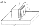
- FIG. 1D shows a schematic perspective view of a semiconductor laser 100 produced according to the first embodiment, which is mounted with its mounting surface 13 on a module carrier 15. Like from the FIG. 1D can be seen - due to the small angle error - the module carrier 3 facing away from the top of the semiconductor laser chip 4 and the mounting surface of the module carrier 15 at a right angle to each other.
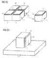
- FIG. 2A shows a schematic perspective view of a first method step of this method.
- a wafer composite 40 of semiconductor laser chips 4 is applied in this embodiment, with its surface facing away from the growth substrate 41 on the provided with Maismetallmaschineen 14 top 31 of a support disk 30.
- the semiconductor laser chips 4 are so-called "bottom-emitter” structures.
- the wafer composite 40 is provided on its surface facing the carrier wafer 30 with a solder metallization, which is soldered or bonded to the contact metallization 14 of the carrier wafer.
- the contact metallization 14, as well as from the FIG. 2A can be seen, have a structuring with separation areas between contact surfaces to the subsequent Separating the composite 70 of wafer composite 40 and carrier plate 30 to facilitate.
- the growth substrate 41 is removed, for example, by selective wet or dry etching. Furthermore, a mesa etching to generate separating regions is carried out between the individual semiconductor laser chips 4 and subsequently an anti-reflective passivation layer is applied to the side of the semiconductor laser chips 4 facing away from the carrier wafer 30, FIG. 2B , In this case, the generation of the mesa structures can alternatively take place prior to the joining of wafer composite 40 and carrier wafer 30 to form a composite 70.
- FIG. 3A shows a schematic sectional view
- FIG. 3B shows a schematic plan view of the semiconductor laser.
- a heat sink 11 is arranged in this embodiment between the mounting block 3 and the semiconductor laser chip 4, which improves the heat dissipation from the semiconductor laser chip 4 to the mounting block 3 in the operation of the semiconductor laser 100.
- the heat sink is applied before the application of the semiconductor laser chips 4 on the support plate 30 and fixed there.
- the heat sinks 11 can be used as Washer in the composite on the support plate 30 or individually applied.
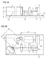
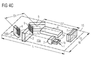
- FIG. 4A shows the semiconductor laser module according to the first embodiment in a schematic side view.
- the FIG. 4B shows the semiconductor laser module in a schematic plan view.
- the FIG. 4C shows the semiconductor laser module in a schematic perspective view.
- the semiconductor laser module comprises a module carrier 15.
- the module carrier 15 is a plate, which consists for example of Direct Bonded Copper (DBC).
- DBC Direct Bonded Copper
- the module carrier can have a base body made of a ceramic material, such as aluminum nitride (AlN), which has metallizations on top and bottom, which consist for example of copper and a thickness of between 0.1 and 0.3, preferably 0.2 mm exhibit.
- the module carrier can contain or consist of silicon.
- the module carrier 15 has a mounting surface 15 a, which is formed by the top of the module carrier 15.
- the base of the mounting surface and thus the base of the module carrier 15 is preferably at most 150 mm 2 , more preferably at most 100 mm 2 .
- the mounting surface 15a has a length L of 11 mm and a width W of 6 mm.
- the pumping device 1 comprises a pumping source 1a and a heat sink 1b.
- the pump source 1a is fixed on the side of the heat sink 1b which is remote from the mounting surface 15a.
- the heat sink 1b is applied with its side facing away from the pump source 1a on the mounting surface 15a, for example, soldered or glued.
- the pump source 1a produces highly divergent pump light.
- the pump source 1a is, for example, an edge-emitting semiconductor laser such as a wide-band laser having at least one emitter region. Pump radiation generated by the pump source during operation is focused onto the semiconductor laser chip 4 by the pump optics 2.
- the semiconductor laser chip 4 is part of the semiconductor laser 100 as in connection with the Figures 1A to 1D . 2A to 2C or 3A, 3B is explained in more detail.
- the semiconductor laser 100 comprises a mounting block 3, which is fastened with its mounting surfaces 13 on the mounting surface 15a of the module carrier 15, for example, soldered or glued.
- the pump radiation 1c is focused on the semiconductor laser chip 4 by the pump optics 2 in such a way that a pump spot with a radius between approximately 25 ⁇ m and at most 60 ⁇ m is generated there.
- the semiconductor laser chip 4 is a surface emitting semiconductor laser chip (VECSEL) which is optically pumped by the pumping source 1a. During operation of the semiconductor laser chip 4, the heat flow through the mounting block 3 takes place through a 90 ° angle to the module carrier 15.
- VECSEL surface emitting semiconductor laser chip
- the resonator of the semiconductor laser module is defined by a Bragg mirror 43 of the semiconductor laser chip 4 and the end mirror 7.
- the reflective surface of the end mirror 7 in this case comprises a coating which is highly reflective for the electromagnetic radiation of the fundamental wavelength generated by the semiconductor laser chip and a coating which is highly reflective for the wavelength-converted by the frequency conversion device 6 electromagnetic radiation.
- the semiconductor laser chip 4 generates, for example, electromagnetic radiation in the spectral range for infrared radiation, which is converted by the frequency conversion device 6 to electromagnetic radiation in the spectral range of green light.
- the pumping light has a wavelength of 808 nm
- the semiconductor laser chip 4 generates radiation of wavelength 1060 nm
- the frequency conversion device 6 generates radiation of the wavelength 530 nm.
- the semiconductor laser module has a height H of at most 3.5 mm, preferably at most 3 mm, particularly preferably at most 2.5 mm.
- the height H is the distance from the underside of the module carrier 15 facing away from the mounting surface 15a to the highest point of the semiconductor laser module which is formed, for example, by a component of the semiconductor laser module such as the semiconductor laser 100.
- the resonator has a length D1 plus D2 which is at most 10 mm.
- a wavelength-selective element for example an etalon 9, is arranged in the resonator. Furthermore, in the resonator, the frequency conversion device 6 is arranged, which comprises an optically non-linear crystal. Moreover, the frequency conversion device 6 may include a heater 6a disposed between the optically nonlinear crystal and the module carrier 15 on mounting surface 15a.
- the decoupling of the frequency-converted laser radiation 8 - for example, the green laser radiation - is performed by the output coupler 5, which also serves as a folding mirror for polarization selection.
- the output coupler 5 has a coating which is highly reflective for electromagnetic radiation of the fundamental wavelength.
- the output coupler 5 has a coating which is designed to be antireflective for frequency-converted radiation. In this way, electromagnetic radiation of the fundamental wavelength is held in the resonator, whereas frequency-converted radiation 8 can leave the semiconductor laser module through the output coupler 5.
- the output coupler 5 is designed in the present embodiment as a plane mirror for the electromagnetic radiation of the fundamental wavelength.
- the end mirror 7 is when in conjunction with the FIGS. 4A to 4C described embodiment, arranged on a mirror mounting block 10, which may for example consist of silicon, glass or aluminum nitride.
- the mirror mounting block is optional.
Landscapes
- Physics & Mathematics (AREA)
- Condensed Matter Physics & Semiconductors (AREA)
- General Physics & Mathematics (AREA)
- Electromagnetism (AREA)
- Optics & Photonics (AREA)
- Semiconductor Lasers (AREA)
Applications Claiming Priority (1)
| Application Number | Priority Date | Filing Date | Title |
|---|---|---|---|
| DE102008009108A DE102008009108A1 (de) | 2008-02-14 | 2008-02-14 | Verfahren zur Herstellung eines Halbleiterlasers sowie Halbleiterlaser |
Publications (3)
| Publication Number | Publication Date |
|---|---|
| EP2091116A2 true EP2091116A2 (fr) | 2009-08-19 |
| EP2091116A3 EP2091116A3 (fr) | 2013-10-02 |
| EP2091116B1 EP2091116B1 (fr) | 2020-04-08 |
Family
ID=40428207
Family Applications (1)
| Application Number | Title | Priority Date | Filing Date |
|---|---|---|---|
| EP09151143.6A Active EP2091116B1 (fr) | 2008-02-14 | 2009-01-22 | Procédé destiné à la fabrication d'un laser semi-conducteur, ainsi que laser semi-conducteur |
Country Status (4)
| Country | Link |
|---|---|
| US (1) | US7995633B2 (fr) |
| EP (1) | EP2091116B1 (fr) |
| JP (1) | JP5517465B2 (fr) |
| DE (1) | DE102008009108A1 (fr) |
Cited By (2)
| Publication number | Priority date | Publication date | Assignee | Title |
|---|---|---|---|---|
| EP2091117A3 (fr) * | 2008-02-14 | 2014-02-19 | OSRAM Opto Semiconductors GmbH | Module laser semi-conducteur |
| WO2014026951A1 (fr) * | 2012-08-13 | 2014-02-20 | Osram Opto Semiconductors Gmbh | Procédé pour fabriquer un élément laser à semi-conducteurs et élément laser à semi-conducteurs |
Families Citing this family (3)
| Publication number | Priority date | Publication date | Assignee | Title |
|---|---|---|---|---|
| KR101715761B1 (ko) | 2010-12-31 | 2017-03-14 | 삼성전자주식회사 | 반도체 패키지 및 그 제조방법 |
| DE102013224420A1 (de) * | 2013-05-13 | 2014-11-13 | Osram Gmbh | Laserbauelement und Verfahren zur seiner Herstellung |
| DE102016101942B4 (de) * | 2016-02-04 | 2022-07-21 | OSRAM Opto Semiconductors Gesellschaft mit beschränkter Haftung | Verfahren zum Herstellen einer optoelektronischen Leuchtvorrichtung |
Citations (1)
| Publication number | Priority date | Publication date | Assignee | Title |
|---|---|---|---|---|
| WO2002067393A1 (fr) | 2001-02-20 | 2002-08-29 | Osram Opto Semiconductors Gmbh | Systeme laser a semi-conducteur a pompage optique a emission par surface et procede permettant de le produire |
Family Cites Families (24)
| Publication number | Priority date | Publication date | Assignee | Title |
|---|---|---|---|---|
| JPH03286547A (ja) * | 1990-04-02 | 1991-12-17 | Mitsubishi Electric Corp | 半導体レーザ装置の製造方法 |
| JPH10335383A (ja) * | 1997-05-28 | 1998-12-18 | Matsushita Electric Ind Co Ltd | 半導体装置の製造方法 |
| JP3810529B2 (ja) * | 1997-09-05 | 2006-08-16 | 株式会社フジクラ | 光部品の組立方法 |
| JP4897133B2 (ja) * | 1999-12-09 | 2012-03-14 | ソニー株式会社 | 半導体発光素子、その製造方法および配設基板 |
| JP2001230492A (ja) * | 2000-02-21 | 2001-08-24 | Fuji Photo Film Co Ltd | 半導体発光装置 |
| EP1277240B1 (fr) * | 2000-04-26 | 2015-05-20 | OSRAM Opto Semiconductors GmbH | Procédé de fabrication d'un composant semi-conducteur emetteur de lumière |
| US6680959B2 (en) * | 2000-07-18 | 2004-01-20 | Rohm Co., Ltd. | Semiconductor light emitting device and semiconductor laser |
| US20030099273A1 (en) * | 2001-01-09 | 2003-05-29 | Murry Stefan J. | Method and apparatus for coupling a surface-emitting laser to an external device |
| JP4242599B2 (ja) * | 2002-04-08 | 2009-03-25 | パナソニック株式会社 | 窒化物半導体装置の製造方法及び窒化物半導体基板の製造方法 |
| US6936929B1 (en) * | 2003-03-17 | 2005-08-30 | National Semiconductor Corporation | Multichip packages with exposed dice |
| JP3794489B2 (ja) * | 2003-06-18 | 2006-07-05 | セイコーエプソン株式会社 | 光通信モジュール及びその製造方法、光通信装置、電子機器 |
| TWI240434B (en) * | 2003-06-24 | 2005-09-21 | Osram Opto Semiconductors Gmbh | Method to produce semiconductor-chips |
| US7164702B1 (en) * | 2003-08-29 | 2007-01-16 | The United States Of America As Represented By The Secretary Of The Army | Optical transmitters and interconnects using surface-emitting lasers and micro-optical elements |
| JP4439313B2 (ja) * | 2004-03-31 | 2010-03-24 | 三洋電機株式会社 | 光学モジュールの製造方法 |
| ATE418806T1 (de) * | 2004-04-02 | 2009-01-15 | Nichia Corp | Nitrid-halbleiterlaservorrichtung |
| JP4614715B2 (ja) * | 2004-08-31 | 2011-01-19 | 三洋電機株式会社 | 半導体レーザ装置およびその製造方法 |
| KR101217590B1 (ko) * | 2004-09-22 | 2013-01-03 | 오스람 옵토 세미컨덕터스 게엠베하 | 히트 싱크 상에서 측면으로 광학적으로 펌핑된 표면발광반도체 레이저 |
| US7932111B2 (en) * | 2005-02-23 | 2011-04-26 | Cree, Inc. | Substrate removal process for high light extraction LEDs |
| DE102005053274A1 (de) * | 2005-09-30 | 2007-04-12 | Osram Opto Semiconductors Gmbh | Verfahren zum Herstellen einer Mehrzahl von Halbleiterchips und Halbleiterbauelement |
| DE102006017293A1 (de) | 2005-12-30 | 2007-07-05 | Osram Opto Semiconductors Gmbh | Verfahren zur Herstellung einer optisch pumpbaren Halbleitervorrichtung |
| DE102006017294A1 (de) * | 2005-12-30 | 2007-07-05 | Osram Opto Semiconductors Gmbh | Optisch pumpbare Halbleitervorrichtung |
| DE102006033502A1 (de) * | 2006-05-03 | 2007-11-15 | Osram Opto Semiconductors Gmbh | Strahlungsemittierender Halbleiterkörper mit Trägersubstrat und Verfahren zur Herstellung eines solchen |
| DE102006042196A1 (de) * | 2006-06-30 | 2008-01-03 | Osram Opto Semiconductors Gmbh | Oberflächenemittierender Halbleiterkörper mit vertikaler Emissionsrichtung und stabilisierter Emissionswellenlänge |
| JP4948307B2 (ja) * | 2006-07-31 | 2012-06-06 | 三洋電機株式会社 | 半導体レーザ素子およびその製造方法 |
-
2008
- 2008-02-14 DE DE102008009108A patent/DE102008009108A1/de not_active Withdrawn
-
2009
- 2009-01-22 EP EP09151143.6A patent/EP2091116B1/fr active Active
- 2009-02-13 US US12/371,292 patent/US7995633B2/en active Active
- 2009-02-13 JP JP2009031414A patent/JP5517465B2/ja not_active Expired - Fee Related
Patent Citations (1)
| Publication number | Priority date | Publication date | Assignee | Title |
|---|---|---|---|---|
| WO2002067393A1 (fr) | 2001-02-20 | 2002-08-29 | Osram Opto Semiconductors Gmbh | Systeme laser a semi-conducteur a pompage optique a emission par surface et procede permettant de le produire |
Cited By (3)
| Publication number | Priority date | Publication date | Assignee | Title |
|---|---|---|---|---|
| EP2091117A3 (fr) * | 2008-02-14 | 2014-02-19 | OSRAM Opto Semiconductors GmbH | Module laser semi-conducteur |
| WO2014026951A1 (fr) * | 2012-08-13 | 2014-02-20 | Osram Opto Semiconductors Gmbh | Procédé pour fabriquer un élément laser à semi-conducteurs et élément laser à semi-conducteurs |
| US9450376B2 (en) | 2012-08-13 | 2016-09-20 | Osram Opto Semiconductors Gmbh | Method of producing a semiconductor laser element, and semiconductor laser element |
Also Published As
| Publication number | Publication date |
|---|---|
| US20090232177A1 (en) | 2009-09-17 |
| JP5517465B2 (ja) | 2014-06-11 |
| EP2091116B1 (fr) | 2020-04-08 |
| EP2091116A3 (fr) | 2013-10-02 |
| DE102008009108A1 (de) | 2009-08-20 |
| US7995633B2 (en) | 2011-08-09 |
| JP2009194388A (ja) | 2009-08-27 |
Similar Documents
| Publication | Publication Date | Title |
|---|---|---|
| EP0905797B1 (fr) | Source lumineuse à semi-conducteur et méthode de fabricaton | |
| EP2149160B1 (fr) | Composant optoélectronique et procédé de fabrication d'une pluralité de composants optoélectroniques | |
| DE19527026C2 (de) | Optoelektronischer Wandler und Herstellverfahren | |
| DE102013112549B4 (de) | Verfahren zur Herstellung von optoelektronischen Halbleiterbauelementen und optoelektronisches Halbleiterbauelement | |
| EP2483937B1 (fr) | Composant optoélectronique | |
| EP2612372B1 (fr) | Puce de diode électroluminescente | |
| DE112013006065B4 (de) | Verfahren zur Herstellung von Halbleiter-Laserelementen und Halbleiter-Laserelement | |
| EP0731509A1 (fr) | Convertisseur optoélectronique et procédé de fabrication | |
| DE112017002426B4 (de) | Verfahren zur Herstellung eines optoelektronischen Bauelements und optoelektronisches Bauelement | |
| EP1299910A1 (fr) | Module del, son procede de production et son utilisation | |
| WO2018134086A1 (fr) | Laser à semi-conducteurs et procédé de fabrication d'un tel laser à semi-conducteurs | |
| WO2014173590A1 (fr) | Procédé de fabrication d'une puce de semi-conducteur optoélectronique et puce de semi-conducteur optoélectronique | |
| DE102005053274A1 (de) | Verfahren zum Herstellen einer Mehrzahl von Halbleiterchips und Halbleiterbauelement | |
| WO2014128003A1 (fr) | Composant optoélectronique | |
| WO2013120646A1 (fr) | Procédé de fabrication d'un composant à semi-conducteur optoélectronique et composant à semi-conducteur optoélectronique | |
| EP2091116B1 (fr) | Procédé destiné à la fabrication d'un laser semi-conducteur, ainsi que laser semi-conducteur | |
| EP2308105B1 (fr) | Élément semi-conducteur optoélectronique | |
| WO1998014818A1 (fr) | Procede pour produire un corps façonne separateur de faisceaux et utilisation de ce dernier dans un module optoelectronique | |
| DE112018005496B4 (de) | Strahlungsemittierendes halbleiterbauelement und verfahren zur herstellung von strahlungsemittierenden halbleiterbauelementen | |
| DE102019131502A1 (de) | Verfahren zur herstellung strahlungsemittierender halbleiterchips, strahlungsemittierender halbleiterchip und strahlungsemittierendes bauelement | |
| DE102008048903B4 (de) | Optoelektronisches Bauteil | |
| DE102012107409B4 (de) | Verfahren zur Herstellung eines Halbleiter-Laserelements | |
| WO2009079982A2 (fr) | Procédé pour produire des puces semi-conductrices et puce semi-conductrice | |
| EP2091117A2 (fr) | Module laser semi-conducteur | |
| WO2025242266A1 (fr) | Procédé de fabrication d'un réseau comprenant des diodes électroluminescentes uv, et réseau |
Legal Events
| Date | Code | Title | Description |
|---|---|---|---|
| PUAI | Public reference made under article 153(3) epc to a published international application that has entered the european phase |
Free format text: ORIGINAL CODE: 0009012 |
|
| AK | Designated contracting states |
Kind code of ref document: A2 Designated state(s): AT BE BG CH CY CZ DE DK EE ES FI FR GB GR HR HU IE IS IT LI LT LU LV MC MK MT NL NO PL PT RO SE SI SK TR |
|
| AX | Request for extension of the european patent |
Extension state: AL BA RS |
|
| RAP1 | Party data changed (applicant data changed or rights of an application transferred) |
Owner name: OSRAM OPTO SEMICONDUCTORS GMBH |
|
| RIN1 | Information on inventor provided before grant (corrected) |
Inventor name: UNOLD, HEIKO Inventor name: DACHS, JUERGEN Inventor name: SCHWARZ, THOMAS Inventor name: SINGER, FRANK Inventor name: ILLEK, STEFAN Inventor name: SCHULZ, ROLAND |
|
| PUAL | Search report despatched |
Free format text: ORIGINAL CODE: 0009013 |
|
| AK | Designated contracting states |
Kind code of ref document: A3 Designated state(s): AT BE BG CH CY CZ DE DK EE ES FI FR GB GR HR HU IE IS IT LI LT LU LV MC MK MT NL NO PL PT RO SE SI SK TR |
|
| AX | Request for extension of the european patent |
Extension state: AL BA RS |
|
| RIC1 | Information provided on ipc code assigned before grant |
Ipc: H01L 33/00 20100101ALI20130828BHEP Ipc: H01S 5/02 20060101AFI20130828BHEP Ipc: H01L 21/78 20060101ALI20130828BHEP |
|
| 17P | Request for examination filed |
Effective date: 20140312 |
|
| RBV | Designated contracting states (corrected) |
Designated state(s): AT BE BG CH CY CZ DE DK EE ES FI FR GB GR HR HU IE IS IT LI LT LU LV MC MK MT NL NO PL PT RO SE SI SK TR |
|
| AKX | Designation fees paid |
Designated state(s): DE |
|
| RBV | Designated contracting states (corrected) |
Designated state(s): AT BE BG CH CY CZ DE DK EE ES FI FR GB GR HR HU IE IS IT LI LT LU LV MC MK MT NL NO PL PT RO SE SI SK TR |
|
| STAA | Information on the status of an ep patent application or granted ep patent |
Free format text: STATUS: EXAMINATION IS IN PROGRESS |
|
| 17Q | First examination report despatched |
Effective date: 20171124 |
|
| RAP1 | Party data changed (applicant data changed or rights of an application transferred) |
Owner name: OSRAM OPTO SEMICONDUCTORS GMBH |
|
| GRAP | Despatch of communication of intention to grant a patent |
Free format text: ORIGINAL CODE: EPIDOSNIGR1 |
|
| STAA | Information on the status of an ep patent application or granted ep patent |
Free format text: STATUS: GRANT OF PATENT IS INTENDED |
|
| INTG | Intention to grant announced |
Effective date: 20191028 |
|
| GRAS | Grant fee paid |
Free format text: ORIGINAL CODE: EPIDOSNIGR3 |
|
| GRAA | (expected) grant |
Free format text: ORIGINAL CODE: 0009210 |
|
| STAA | Information on the status of an ep patent application or granted ep patent |
Free format text: STATUS: THE PATENT HAS BEEN GRANTED |
|
| AK | Designated contracting states |
Kind code of ref document: B1 Designated state(s): AT BE BG CH CY CZ DE DK EE ES FI FR GB GR HR HU IE IS IT LI LT LU LV MC MK MT NL NO PL PT RO SE SI SK TR |
|
| REG | Reference to a national code |
Ref country code: GB Ref legal event code: FG4D Free format text: NOT ENGLISH |
|
| REG | Reference to a national code |
Ref country code: AT Ref legal event code: REF Ref document number: 1255628 Country of ref document: AT Kind code of ref document: T Effective date: 20200415 Ref country code: CH Ref legal event code: EP |
|
| REG | Reference to a national code |
Ref country code: IE Ref legal event code: FG4D Free format text: LANGUAGE OF EP DOCUMENT: GERMAN |
|
| REG | Reference to a national code |
Ref country code: DE Ref legal event code: R096 Ref document number: 502009016157 Country of ref document: DE |
|
| REG | Reference to a national code |
Ref country code: NL Ref legal event code: MP Effective date: 20200408 |
|
| REG | Reference to a national code |
Ref country code: LT Ref legal event code: MG4D |
|
| PG25 | Lapsed in a contracting state [announced via postgrant information from national office to epo] |
Ref country code: NL Free format text: LAPSE BECAUSE OF FAILURE TO SUBMIT A TRANSLATION OF THE DESCRIPTION OR TO PAY THE FEE WITHIN THE PRESCRIBED TIME-LIMIT Effective date: 20200408 Ref country code: PT Free format text: LAPSE BECAUSE OF FAILURE TO SUBMIT A TRANSLATION OF THE DESCRIPTION OR TO PAY THE FEE WITHIN THE PRESCRIBED TIME-LIMIT Effective date: 20200817 Ref country code: FI Free format text: LAPSE BECAUSE OF FAILURE TO SUBMIT A TRANSLATION OF THE DESCRIPTION OR TO PAY THE FEE WITHIN THE PRESCRIBED TIME-LIMIT Effective date: 20200408 Ref country code: IS Free format text: LAPSE BECAUSE OF FAILURE TO SUBMIT A TRANSLATION OF THE DESCRIPTION OR TO PAY THE FEE WITHIN THE PRESCRIBED TIME-LIMIT Effective date: 20200808 Ref country code: SE Free format text: LAPSE BECAUSE OF FAILURE TO SUBMIT A TRANSLATION OF THE DESCRIPTION OR TO PAY THE FEE WITHIN THE PRESCRIBED TIME-LIMIT Effective date: 20200408 Ref country code: GR Free format text: LAPSE BECAUSE OF FAILURE TO SUBMIT A TRANSLATION OF THE DESCRIPTION OR TO PAY THE FEE WITHIN THE PRESCRIBED TIME-LIMIT Effective date: 20200709 Ref country code: NO Free format text: LAPSE BECAUSE OF FAILURE TO SUBMIT A TRANSLATION OF THE DESCRIPTION OR TO PAY THE FEE WITHIN THE PRESCRIBED TIME-LIMIT Effective date: 20200708 Ref country code: LT Free format text: LAPSE BECAUSE OF FAILURE TO SUBMIT A TRANSLATION OF THE DESCRIPTION OR TO PAY THE FEE WITHIN THE PRESCRIBED TIME-LIMIT Effective date: 20200408 |
|
| PG25 | Lapsed in a contracting state [announced via postgrant information from national office to epo] |
Ref country code: LV Free format text: LAPSE BECAUSE OF FAILURE TO SUBMIT A TRANSLATION OF THE DESCRIPTION OR TO PAY THE FEE WITHIN THE PRESCRIBED TIME-LIMIT Effective date: 20200408 Ref country code: BG Free format text: LAPSE BECAUSE OF FAILURE TO SUBMIT A TRANSLATION OF THE DESCRIPTION OR TO PAY THE FEE WITHIN THE PRESCRIBED TIME-LIMIT Effective date: 20200708 Ref country code: HR Free format text: LAPSE BECAUSE OF FAILURE TO SUBMIT A TRANSLATION OF THE DESCRIPTION OR TO PAY THE FEE WITHIN THE PRESCRIBED TIME-LIMIT Effective date: 20200408 |
|
| REG | Reference to a national code |
Ref country code: DE Ref legal event code: R097 Ref document number: 502009016157 Country of ref document: DE |
|
| PG25 | Lapsed in a contracting state [announced via postgrant information from national office to epo] |
Ref country code: ES Free format text: LAPSE BECAUSE OF FAILURE TO SUBMIT A TRANSLATION OF THE DESCRIPTION OR TO PAY THE FEE WITHIN THE PRESCRIBED TIME-LIMIT Effective date: 20200408 Ref country code: CZ Free format text: LAPSE BECAUSE OF FAILURE TO SUBMIT A TRANSLATION OF THE DESCRIPTION OR TO PAY THE FEE WITHIN THE PRESCRIBED TIME-LIMIT Effective date: 20200408 Ref country code: RO Free format text: LAPSE BECAUSE OF FAILURE TO SUBMIT A TRANSLATION OF THE DESCRIPTION OR TO PAY THE FEE WITHIN THE PRESCRIBED TIME-LIMIT Effective date: 20200408 Ref country code: EE Free format text: LAPSE BECAUSE OF FAILURE TO SUBMIT A TRANSLATION OF THE DESCRIPTION OR TO PAY THE FEE WITHIN THE PRESCRIBED TIME-LIMIT Effective date: 20200408 Ref country code: DK Free format text: LAPSE BECAUSE OF FAILURE TO SUBMIT A TRANSLATION OF THE DESCRIPTION OR TO PAY THE FEE WITHIN THE PRESCRIBED TIME-LIMIT Effective date: 20200408 Ref country code: IT Free format text: LAPSE BECAUSE OF FAILURE TO SUBMIT A TRANSLATION OF THE DESCRIPTION OR TO PAY THE FEE WITHIN THE PRESCRIBED TIME-LIMIT Effective date: 20200408 |
|
| PLBE | No opposition filed within time limit |
Free format text: ORIGINAL CODE: 0009261 |
|
| STAA | Information on the status of an ep patent application or granted ep patent |
Free format text: STATUS: NO OPPOSITION FILED WITHIN TIME LIMIT |
|
| PG25 | Lapsed in a contracting state [announced via postgrant information from national office to epo] |
Ref country code: PL Free format text: LAPSE BECAUSE OF FAILURE TO SUBMIT A TRANSLATION OF THE DESCRIPTION OR TO PAY THE FEE WITHIN THE PRESCRIBED TIME-LIMIT Effective date: 20200408 Ref country code: SK Free format text: LAPSE BECAUSE OF FAILURE TO SUBMIT A TRANSLATION OF THE DESCRIPTION OR TO PAY THE FEE WITHIN THE PRESCRIBED TIME-LIMIT Effective date: 20200408 |
|
| 26N | No opposition filed |
Effective date: 20210112 |
|
| PG25 | Lapsed in a contracting state [announced via postgrant information from national office to epo] |
Ref country code: SI Free format text: LAPSE BECAUSE OF FAILURE TO SUBMIT A TRANSLATION OF THE DESCRIPTION OR TO PAY THE FEE WITHIN THE PRESCRIBED TIME-LIMIT Effective date: 20200408 |
|
| PG25 | Lapsed in a contracting state [announced via postgrant information from national office to epo] |
Ref country code: MC Free format text: LAPSE BECAUSE OF FAILURE TO SUBMIT A TRANSLATION OF THE DESCRIPTION OR TO PAY THE FEE WITHIN THE PRESCRIBED TIME-LIMIT Effective date: 20200408 |
|
| REG | Reference to a national code |
Ref country code: CH Ref legal event code: PL |
|
| GBPC | Gb: european patent ceased through non-payment of renewal fee |
Effective date: 20210122 |
|
| PG25 | Lapsed in a contracting state [announced via postgrant information from national office to epo] |
Ref country code: LU Free format text: LAPSE BECAUSE OF NON-PAYMENT OF DUE FEES Effective date: 20210122 |
|
| REG | Reference to a national code |
Ref country code: BE Ref legal event code: MM Effective date: 20210131 |
|
| PG25 | Lapsed in a contracting state [announced via postgrant information from national office to epo] |
Ref country code: FR Free format text: LAPSE BECAUSE OF NON-PAYMENT OF DUE FEES Effective date: 20210131 |
|
| PG25 | Lapsed in a contracting state [announced via postgrant information from national office to epo] |
Ref country code: LI Free format text: LAPSE BECAUSE OF NON-PAYMENT OF DUE FEES Effective date: 20210131 Ref country code: CH Free format text: LAPSE BECAUSE OF NON-PAYMENT OF DUE FEES Effective date: 20210131 Ref country code: GB Free format text: LAPSE BECAUSE OF NON-PAYMENT OF DUE FEES Effective date: 20210122 |
|
| PG25 | Lapsed in a contracting state [announced via postgrant information from national office to epo] |
Ref country code: IE Free format text: LAPSE BECAUSE OF NON-PAYMENT OF DUE FEES Effective date: 20210122 |
|
| REG | Reference to a national code |
Ref country code: AT Ref legal event code: MM01 Ref document number: 1255628 Country of ref document: AT Kind code of ref document: T Effective date: 20210122 |
|
| PG25 | Lapsed in a contracting state [announced via postgrant information from national office to epo] |
Ref country code: AT Free format text: LAPSE BECAUSE OF NON-PAYMENT OF DUE FEES Effective date: 20210122 |
|
| PG25 | Lapsed in a contracting state [announced via postgrant information from national office to epo] |
Ref country code: BE Free format text: LAPSE BECAUSE OF NON-PAYMENT OF DUE FEES Effective date: 20210131 |
|
| PG25 | Lapsed in a contracting state [announced via postgrant information from national office to epo] |
Ref country code: HU Free format text: LAPSE BECAUSE OF FAILURE TO SUBMIT A TRANSLATION OF THE DESCRIPTION OR TO PAY THE FEE WITHIN THE PRESCRIBED TIME-LIMIT; INVALID AB INITIO Effective date: 20090122 Ref country code: CY Free format text: LAPSE BECAUSE OF FAILURE TO SUBMIT A TRANSLATION OF THE DESCRIPTION OR TO PAY THE FEE WITHIN THE PRESCRIBED TIME-LIMIT Effective date: 20200408 |
|
| P01 | Opt-out of the competence of the unified patent court (upc) registered |
Effective date: 20230825 |
|
| PG25 | Lapsed in a contracting state [announced via postgrant information from national office to epo] |
Ref country code: MK Free format text: LAPSE BECAUSE OF FAILURE TO SUBMIT A TRANSLATION OF THE DESCRIPTION OR TO PAY THE FEE WITHIN THE PRESCRIBED TIME-LIMIT Effective date: 20200408 |
|
| PG25 | Lapsed in a contracting state [announced via postgrant information from national office to epo] |
Ref country code: TR Free format text: LAPSE BECAUSE OF FAILURE TO SUBMIT A TRANSLATION OF THE DESCRIPTION OR TO PAY THE FEE WITHIN THE PRESCRIBED TIME-LIMIT Effective date: 20200408 |
|
| PG25 | Lapsed in a contracting state [announced via postgrant information from national office to epo] |
Ref country code: MT Free format text: LAPSE BECAUSE OF FAILURE TO SUBMIT A TRANSLATION OF THE DESCRIPTION OR TO PAY THE FEE WITHIN THE PRESCRIBED TIME-LIMIT Effective date: 20200408 |
|
| PGFP | Annual fee paid to national office [announced via postgrant information from national office to epo] |
Ref country code: DE Payment date: 20260121 Year of fee payment: 18 |