EP2096676A1 - Verfahren zur Herstellung einer Halbleitervorrichtung mit vergrabenem Gitter und entsprechende integrierte Halbleiterschaltung - Google Patents
Verfahren zur Herstellung einer Halbleitervorrichtung mit vergrabenem Gitter und entsprechende integrierte Halbleiterschaltung Download PDFInfo
- Publication number
- EP2096676A1 EP2096676A1 EP09153744A EP09153744A EP2096676A1 EP 2096676 A1 EP2096676 A1 EP 2096676A1 EP 09153744 A EP09153744 A EP 09153744A EP 09153744 A EP09153744 A EP 09153744A EP 2096676 A1 EP2096676 A1 EP 2096676A1
- Authority
- EP
- European Patent Office
- Prior art keywords
- semiconductor
- region
- gate
- aluminum
- layer
- Prior art date
- Legal status (The legal status is an assumption and is not a legal conclusion. Google has not performed a legal analysis and makes no representation as to the accuracy of the status listed.)
- Withdrawn
Links
Images








Classifications
-
- H—ELECTRICITY
- H10—SEMICONDUCTOR DEVICES; ELECTRIC SOLID-STATE DEVICES NOT OTHERWISE PROVIDED FOR
- H10D—INORGANIC ELECTRIC SEMICONDUCTOR DEVICES
- H10D30/00—Field-effect transistors [FET]
- H10D30/60—Insulated-gate field-effect transistors [IGFET]
- H10D30/67—Thin-film transistors [TFT]
- H10D30/6729—Thin-film transistors [TFT] characterised by the electrodes
- H10D30/6737—Thin-film transistors [TFT] characterised by the electrodes characterised by the electrode materials
- H10D30/6739—Conductor-insulator-semiconductor electrodes
-
- H—ELECTRICITY
- H10—SEMICONDUCTOR DEVICES; ELECTRIC SOLID-STATE DEVICES NOT OTHERWISE PROVIDED FOR
- H10D—INORGANIC ELECTRIC SEMICONDUCTOR DEVICES
- H10D30/00—Field-effect transistors [FET]
- H10D30/01—Manufacture or treatment
- H10D30/021—Manufacture or treatment of FETs having insulated gates [IGFET]
- H10D30/026—Manufacture or treatment of FETs having insulated gates [IGFET] having laterally-coplanar source and drain regions, a gate at the sides of the bulk channel, and both horizontal and vertical current flow
-
- H—ELECTRICITY
- H10—SEMICONDUCTOR DEVICES; ELECTRIC SOLID-STATE DEVICES NOT OTHERWISE PROVIDED FOR
- H10D—INORGANIC ELECTRIC SEMICONDUCTOR DEVICES
- H10D30/00—Field-effect transistors [FET]
- H10D30/60—Insulated-gate field-effect transistors [IGFET]
- H10D30/67—Thin-film transistors [TFT]
- H10D30/6729—Thin-film transistors [TFT] characterised by the electrodes
- H10D30/673—Thin-film transistors [TFT] characterised by the electrodes characterised by the shapes, relative sizes or dispositions of the gate electrodes
- H10D30/6735—Thin-film transistors [TFT] characterised by the electrodes characterised by the shapes, relative sizes or dispositions of the gate electrodes having gates fully surrounding the channels, e.g. gate-all-around
-
- H—ELECTRICITY
- H10—SEMICONDUCTOR DEVICES; ELECTRIC SOLID-STATE DEVICES NOT OTHERWISE PROVIDED FOR
- H10D—INORGANIC ELECTRIC SEMICONDUCTOR DEVICES
- H10D30/00—Field-effect transistors [FET]
- H10D30/60—Insulated-gate field-effect transistors [IGFET]
- H10D30/67—Thin-film transistors [TFT]
- H10D30/6757—Thin-film transistors [TFT] characterised by the structure of the channel, e.g. transverse or longitudinal shape or doping profile
Definitions
- Buried grid devices are particularly interesting for channel lengths of less than 50 nanometers, because they make it possible to suppress so-called short channel effects while at the same time making it possible to obtain a current intensity. Doubled or tripled compared to a conventional transistor. It is recalled here that a short channel has a very small distance (length) between the source and the drain, and that the "short channel” effect results in a decrease in the threshold voltage of the transistor, which can extreme limit lead to obtaining a transistor very difficult to control and lead to the mode "piercing".
- buried grid devices comprise a grid made from poly-silicon.
- a poly-silicon gate reveals numerous limitations such as poly-depletion, incompatibility with dielectrics with high permittivity, and too high gate resistivity.
- the cavity may thus have a high form factor, that is to say present, for example, a dimension much greater than the other two.
- the cavity may be accessible by a lateral surface whose sides are the two small dimensions, while the upper wall and the lower wall comprise the much larger dimension.
- the first material is, for example, poly-silicon or poly-silicon-germanium.
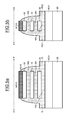
- the filling of the cavity with poly-silicon or poly-silicon-germanium can be carried out according to a method known to those skilled in the art, for example by atomic layer deposition ALD (in English: “Atomic Layer Deposition Or CVD chemical vapor deposition ("Chemical Vapor Deposition"). It is preferably deposited at the time of formation of the gate region, and is not already present before the gate material forming steps.
- ALD atomic layer deposition
- CVD chemical vapor deposition
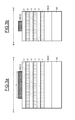
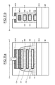
- the stack is itself surmounted by a hard mask layer MD1, for example a silicon nitride layer, conventionally produced by deposition.
- a hard mask layer MD1 for example a silicon nitride layer, conventionally produced by deposition.
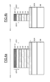
- oxidizing chemistry such as a 40 ml HNO 3 70% + 20 ml H 2 O 2 + 5 ml HF 0.5% solution, or an isotropic plasma etching.
- Si 1-x Ge x alloys are recommended because they are readily removable selectively by such oxidative chemistry or by isotropic plasma etching. These alloys also facilitate the epitaxial production of the initial thin layers of silicon 1, 3 and 5.
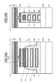
- This layer of insulating dielectric material OX can be obtained for example by a high temperature deposition of a TEOS oxide film.
- a TEOS oxide film can be obtained for example by a high temperature deposition of a TEOS oxide film.
- BSG Silicon Glass "in English language) which has a better etch selectivity with respect to the oxide of the BOX layer, than that of a TEOS oxide.
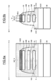
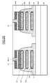
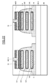
- the relative proportion of germanium with respect to the silicon in the gate region 10 makes it possible to adjust the output work of the alloy, and therefore the threshold voltage of the PMOS device.
- the duration of the annealing makes it possible to adjust the relative proportion of germanium in the gate alloy 13 and therefore the threshold voltage of the semiconductor device.
Landscapes
- Metal-Oxide And Bipolar Metal-Oxide Semiconductor Integrated Circuits (AREA)
- Insulated Gate Type Field-Effect Transistor (AREA)
- Electrodes Of Semiconductors (AREA)
Applications Claiming Priority (1)
| Application Number | Priority Date | Filing Date | Title |
|---|---|---|---|
| FR0851265A FR2928028B1 (fr) | 2008-02-27 | 2008-02-27 | Procede de fabrication d'un dispositif semi-conducteur a grille enterree et circuit integre correspondant. |
Publications (1)
| Publication Number | Publication Date |
|---|---|
| EP2096676A1 true EP2096676A1 (de) | 2009-09-02 |
Family
ID=39863134
Family Applications (1)
| Application Number | Title | Priority Date | Filing Date |
|---|---|---|---|
| EP09153744A Withdrawn EP2096676A1 (de) | 2008-02-27 | 2009-02-26 | Verfahren zur Herstellung einer Halbleitervorrichtung mit vergrabenem Gitter und entsprechende integrierte Halbleiterschaltung |
Country Status (3)
| Country | Link |
|---|---|
| US (1) | US8039332B2 (de) |
| EP (1) | EP2096676A1 (de) |
| FR (1) | FR2928028B1 (de) |
Families Citing this family (56)
| Publication number | Priority date | Publication date | Assignee | Title |
|---|---|---|---|---|
| US8273617B2 (en) | 2009-09-30 | 2012-09-25 | Suvolta, Inc. | Electronic devices and systems, and methods for making and using the same |
| US8421162B2 (en) | 2009-09-30 | 2013-04-16 | Suvolta, Inc. | Advanced transistors with punch through suppression |
| KR101460086B1 (ko) * | 2009-12-15 | 2014-11-10 | 소이텍 | 기판의 재활용 공정 |
| US8530286B2 (en) | 2010-04-12 | 2013-09-10 | Suvolta, Inc. | Low power semiconductor transistor structure and method of fabrication thereof |
| US8569128B2 (en) | 2010-06-21 | 2013-10-29 | Suvolta, Inc. | Semiconductor structure and method of fabrication thereof with mixed metal types |
| US8759872B2 (en) | 2010-06-22 | 2014-06-24 | Suvolta, Inc. | Transistor with threshold voltage set notch and method of fabrication thereof |
| US8377783B2 (en) | 2010-09-30 | 2013-02-19 | Suvolta, Inc. | Method for reducing punch-through in a transistor device |
| US8404551B2 (en) | 2010-12-03 | 2013-03-26 | Suvolta, Inc. | Source/drain extension control for advanced transistors |
| US8461875B1 (en) | 2011-02-18 | 2013-06-11 | Suvolta, Inc. | Digital circuits having improved transistors, and methods therefor |
| US8525271B2 (en) | 2011-03-03 | 2013-09-03 | Suvolta, Inc. | Semiconductor structure with improved channel stack and method for fabrication thereof |
| US8400219B2 (en) | 2011-03-24 | 2013-03-19 | Suvolta, Inc. | Analog circuits having improved transistors, and methods therefor |
| US8748270B1 (en) | 2011-03-30 | 2014-06-10 | Suvolta, Inc. | Process for manufacturing an improved analog transistor |
| US8796048B1 (en) | 2011-05-11 | 2014-08-05 | Suvolta, Inc. | Monitoring and measurement of thin film layers |
| US8999861B1 (en) | 2011-05-11 | 2015-04-07 | Suvolta, Inc. | Semiconductor structure with substitutional boron and method for fabrication thereof |
| US8811068B1 (en) | 2011-05-13 | 2014-08-19 | Suvolta, Inc. | Integrated circuit devices and methods |
| US8569156B1 (en) | 2011-05-16 | 2013-10-29 | Suvolta, Inc. | Reducing or eliminating pre-amorphization in transistor manufacture |
| US8735987B1 (en) | 2011-06-06 | 2014-05-27 | Suvolta, Inc. | CMOS gate stack structures and processes |
| US8995204B2 (en) | 2011-06-23 | 2015-03-31 | Suvolta, Inc. | Circuit devices and methods having adjustable transistor body bias |
| US8629016B1 (en) | 2011-07-26 | 2014-01-14 | Suvolta, Inc. | Multiple transistor types formed in a common epitaxial layer by differential out-diffusion from a doped underlayer |
| KR101891373B1 (ko) | 2011-08-05 | 2018-08-24 | 엠아이이 후지쯔 세미컨덕터 리미티드 | 핀 구조물을 갖는 반도체 디바이스 및 그 제조 방법 |
| US8748986B1 (en) | 2011-08-05 | 2014-06-10 | Suvolta, Inc. | Electronic device with controlled threshold voltage |
| US8645878B1 (en) | 2011-08-23 | 2014-02-04 | Suvolta, Inc. | Porting a circuit design from a first semiconductor process to a second semiconductor process |
| US8614128B1 (en) | 2011-08-23 | 2013-12-24 | Suvolta, Inc. | CMOS structures and processes based on selective thinning |
| US8713511B1 (en) | 2011-09-16 | 2014-04-29 | Suvolta, Inc. | Tools and methods for yield-aware semiconductor manufacturing process target generation |
| US9236466B1 (en) | 2011-10-07 | 2016-01-12 | Mie Fujitsu Semiconductor Limited | Analog circuits having improved insulated gate transistors, and methods therefor |
| US8895327B1 (en) | 2011-12-09 | 2014-11-25 | Suvolta, Inc. | Tipless transistors, short-tip transistors, and methods and circuits therefor |
| US8819603B1 (en) | 2011-12-15 | 2014-08-26 | Suvolta, Inc. | Memory circuits and methods of making and designing the same |
| US8883600B1 (en) | 2011-12-22 | 2014-11-11 | Suvolta, Inc. | Transistor having reduced junction leakage and methods of forming thereof |
| US8599623B1 (en) | 2011-12-23 | 2013-12-03 | Suvolta, Inc. | Circuits and methods for measuring circuit elements in an integrated circuit device |
| US8970289B1 (en) | 2012-01-23 | 2015-03-03 | Suvolta, Inc. | Circuits and devices for generating bi-directional body bias voltages, and methods therefor |
| US8877619B1 (en) | 2012-01-23 | 2014-11-04 | Suvolta, Inc. | Process for manufacture of integrated circuits with different channel doping transistor architectures and devices therefrom |
| US9093550B1 (en) | 2012-01-31 | 2015-07-28 | Mie Fujitsu Semiconductor Limited | Integrated circuits having a plurality of high-K metal gate FETs with various combinations of channel foundation structure and gate stack structure and methods of making same |
| US9406567B1 (en) | 2012-02-28 | 2016-08-02 | Mie Fujitsu Semiconductor Limited | Method for fabricating multiple transistor devices on a substrate with varying threshold voltages |
| US8863064B1 (en) | 2012-03-23 | 2014-10-14 | Suvolta, Inc. | SRAM cell layout structure and devices therefrom |
| US9299698B2 (en) | 2012-06-27 | 2016-03-29 | Mie Fujitsu Semiconductor Limited | Semiconductor structure with multiple transistors having various threshold voltages |
| US8637955B1 (en) | 2012-08-31 | 2014-01-28 | Suvolta, Inc. | Semiconductor structure with reduced junction leakage and method of fabrication thereof |
| US9112057B1 (en) | 2012-09-18 | 2015-08-18 | Mie Fujitsu Semiconductor Limited | Semiconductor devices with dopant migration suppression and method of fabrication thereof |
| US9041126B2 (en) | 2012-09-21 | 2015-05-26 | Mie Fujitsu Semiconductor Limited | Deeply depleted MOS transistors having a screening layer and methods thereof |
| WO2014071049A2 (en) | 2012-10-31 | 2014-05-08 | Suvolta, Inc. | Dram-type device with low variation transistor peripheral circuits, and related methods |
| US8816754B1 (en) | 2012-11-02 | 2014-08-26 | Suvolta, Inc. | Body bias circuits and methods |
| US9093997B1 (en) | 2012-11-15 | 2015-07-28 | Mie Fujitsu Semiconductor Limited | Slew based process and bias monitors and related methods |
| US9070477B1 (en) | 2012-12-12 | 2015-06-30 | Mie Fujitsu Semiconductor Limited | Bit interleaved low voltage static random access memory (SRAM) and related methods |
| US9112484B1 (en) | 2012-12-20 | 2015-08-18 | Mie Fujitsu Semiconductor Limited | Integrated circuit process and bias monitors and related methods |
| US9268885B1 (en) | 2013-02-28 | 2016-02-23 | Mie Fujitsu Semiconductor Limited | Integrated circuit device methods and models with predicted device metric variations |
| US8994415B1 (en) | 2013-03-01 | 2015-03-31 | Suvolta, Inc. | Multiple VDD clock buffer |
| US8988153B1 (en) | 2013-03-09 | 2015-03-24 | Suvolta, Inc. | Ring oscillator with NMOS or PMOS variation insensitivity |
| US9299801B1 (en) | 2013-03-14 | 2016-03-29 | Mie Fujitsu Semiconductor Limited | Method for fabricating a transistor device with a tuned dopant profile |
| US9449967B1 (en) | 2013-03-15 | 2016-09-20 | Fujitsu Semiconductor Limited | Transistor array structure |
| US9112495B1 (en) | 2013-03-15 | 2015-08-18 | Mie Fujitsu Semiconductor Limited | Integrated circuit device body bias circuits and methods |
| US9478571B1 (en) | 2013-05-24 | 2016-10-25 | Mie Fujitsu Semiconductor Limited | Buried channel deeply depleted channel transistor |
| US8976575B1 (en) | 2013-08-29 | 2015-03-10 | Suvolta, Inc. | SRAM performance monitor |
| US9710006B2 (en) | 2014-07-25 | 2017-07-18 | Mie Fujitsu Semiconductor Limited | Power up body bias circuits and methods |
| US9319013B2 (en) | 2014-08-19 | 2016-04-19 | Mie Fujitsu Semiconductor Limited | Operational amplifier input offset correction with transistor threshold voltage adjustment |
| US9391163B2 (en) | 2014-10-03 | 2016-07-12 | International Business Machines Corporation | Stacked planar double-gate lamellar field-effect transistor |
| TWI769245B (zh) * | 2017-04-27 | 2022-07-01 | 日商東京威力科創股份有限公司 | N型場效電晶體與p型場效電晶體奈米線裝置的製造方法 |
| KR102757508B1 (ko) | 2020-08-05 | 2025-01-20 | 삼성전자주식회사 | 반도체 메모리 소자 |
Citations (6)
| Publication number | Priority date | Publication date | Assignee | Title |
|---|---|---|---|---|
| FR2853454A1 (fr) * | 2003-04-03 | 2004-10-08 | St Microelectronics Sa | Transistor mos haute densite |
| US20050029603A1 (en) * | 2003-08-05 | 2005-02-10 | Bin Yu | Varying carrier mobility in semiconductor devices to achieve overall design goals |
| JP2005123404A (ja) * | 2003-10-16 | 2005-05-12 | Fujitsu Ltd | トランジスタ及びその製造方法 |
| US20050224889A1 (en) * | 2004-04-09 | 2005-10-13 | Chang-Woo Oh | Surrounded-channel transistors with directionally etched gate or insulator formation regions and methods of fabrication therefor |
| US20050266645A1 (en) * | 2004-05-25 | 2005-12-01 | Jin-Jun Park | Phosphorous doping methods of manufacturing field effect transistors having multiple stacked channels |
| US20060024874A1 (en) * | 2004-07-30 | 2006-02-02 | Eun-Jung Yun | Methods of forming a multi-bridge-channel MOSFET |
Family Cites Families (12)
| Publication number | Priority date | Publication date | Assignee | Title |
|---|---|---|---|---|
| US4803539A (en) | 1985-03-29 | 1989-02-07 | International Business Machines Corporation | Dopant control of metal silicide formation |
| US6315979B1 (en) * | 1998-06-02 | 2001-11-13 | The Dow Chemical Company | Radioiodinated sulfonated phenols for brachytherapy |
| DE19924571C2 (de) | 1999-05-28 | 2001-03-15 | Siemens Ag | Verfahren zur Herstellung eines Doppel-Gate-MOSFET-Transistors |
| DE19928564A1 (de) | 1999-06-22 | 2001-01-04 | Infineon Technologies Ag | Mehrkanal-MOSFET und Verfahren zu seiner Herstellung |
| US20030054637A1 (en) | 2001-09-20 | 2003-03-20 | Macronix International Co., Ltd. | Method for forming silicide |
| US6661044B2 (en) | 2001-10-22 | 2003-12-09 | Winbond Electronics Corp. | Method of manufacturing MOSEFT and structure thereof |
| FR2845201B1 (fr) | 2002-09-27 | 2005-08-05 | St Microelectronics Sa | Procede de formation de portions d'un materiau compose a l'interieur d'une cavite et circuit electrique incorporant des portions de materiau compose ainsi obtenues |
| JP3962009B2 (ja) | 2003-12-05 | 2007-08-22 | 株式会社東芝 | 半導体装置の製造方法 |
| KR100526887B1 (ko) | 2004-02-10 | 2005-11-09 | 삼성전자주식회사 | 전계효과 트랜지스터 및 그의 제조방법 |
| JP2006278369A (ja) | 2005-03-28 | 2006-10-12 | Fujitsu Ltd | 半導体装置の製造方法 |
| KR100718149B1 (ko) | 2006-02-07 | 2007-05-14 | 삼성전자주식회사 | 게이트-올-어라운드 구조의 반도체 소자 |
| US7749898B2 (en) | 2008-06-24 | 2010-07-06 | Globalfoundries Inc. | Silicide interconnect structure |
-
2008
- 2008-02-27 FR FR0851265A patent/FR2928028B1/fr active Active
-
2009
- 2009-02-12 US US12/370,304 patent/US8039332B2/en active Active
- 2009-02-26 EP EP09153744A patent/EP2096676A1/de not_active Withdrawn
Patent Citations (6)
| Publication number | Priority date | Publication date | Assignee | Title |
|---|---|---|---|---|
| FR2853454A1 (fr) * | 2003-04-03 | 2004-10-08 | St Microelectronics Sa | Transistor mos haute densite |
| US20050029603A1 (en) * | 2003-08-05 | 2005-02-10 | Bin Yu | Varying carrier mobility in semiconductor devices to achieve overall design goals |
| JP2005123404A (ja) * | 2003-10-16 | 2005-05-12 | Fujitsu Ltd | トランジスタ及びその製造方法 |
| US20050224889A1 (en) * | 2004-04-09 | 2005-10-13 | Chang-Woo Oh | Surrounded-channel transistors with directionally etched gate or insulator formation regions and methods of fabrication therefor |
| US20050266645A1 (en) * | 2004-05-25 | 2005-12-01 | Jin-Jun Park | Phosphorous doping methods of manufacturing field effect transistors having multiple stacked channels |
| US20060024874A1 (en) * | 2004-07-30 | 2006-02-02 | Eun-Jung Yun | Methods of forming a multi-bridge-channel MOSFET |
Non-Patent Citations (1)
| Title |
|---|
| "Characteristics of Aluminum Substitution Technology for Self-Aligned Full Metal Gate nMOSFETs", IEEE TRANSACTIONS ON ELECTRON DEVICES, vol. 52, no. 5, May 2005 (2005-05-01) |
Also Published As
| Publication number | Publication date |
|---|---|
| US20090212333A1 (en) | 2009-08-27 |
| US8039332B2 (en) | 2011-10-18 |
| FR2928028A1 (fr) | 2009-08-28 |
| FR2928028B1 (fr) | 2011-07-15 |
Similar Documents
| Publication | Publication Date | Title |
|---|---|---|
| EP2096676A1 (de) | Verfahren zur Herstellung einer Halbleitervorrichtung mit vergrabenem Gitter und entsprechende integrierte Halbleiterschaltung | |
| EP2643848B1 (de) | Verfahren zur herstellung eines feldeffekttransistors in einem netzwerk aus vertikalen nanodrähten | |
| EP1837916B1 (de) | Verfahren zum Herstellen eines Transistors mit einem Germanium enthaltenden Kanal | |
| FR2838238A1 (fr) | Dispositif semiconducteur a grille enveloppante encapsule dans un milieu isolant | |
| EP2323160A1 (de) | Verfahren zur Herstellung von Feldeffekttransistoren mit einer Gegenelektrode und Halbleitervorrichtung | |
| FR2823010A1 (fr) | Procede de fabrication d'un transistor vertical a grille isolee a quadruple canal de conduction, et circuit integre comportant un tel transistor | |
| FR2799305A1 (fr) | Procede de fabrication d'un dispositif semi-conducteur a grille enveloppante et dispositif obtenu | |
| FR2806832A1 (fr) | Transistor mos a source et drain metalliques, et procede de fabrication d'un tel transistor | |
| FR2757312A1 (fr) | Transistor mis a grille metallique auto-alignee et son procede de fabrication | |
| EP2562804B1 (de) | Herstellungsverfahren für ein Bauelement mit durch Silizidierung von Source- und Drain-Gebieten vorgespannten Transistoren, und Bauelement | |
| EP3654394A1 (de) | Transistor mit quellenblöcken und siliciden-drains in der nähe des kanals | |
| FR2928029A1 (fr) | Procede de fabrication d'un dispositif semi-conducteur a grille enterree et circuit integre correspondant. | |
| FR2891664A1 (fr) | Transistor mos vertical et procede de fabrication | |
| EP0635880B1 (de) | Verfahren zur Herstellung eines Transistors in Silizium-auf-Isolator Technologie | |
| EP2120258B1 (de) | Herstellungsverfahren eines Transistors mit Metallquelle und -abfluss | |
| EP1589572A1 (de) | Verfahren zur Herstellung einer integrierten Schaltung mit einem Isolationsgraben und entsprechende integrierte Schaltung | |
| FR2799307A1 (fr) | Dispositif semi-conducteur combinant les avantages des architectures massives et soi, procede de fabrication | |
| WO2011114046A1 (fr) | Procédé de réalisation d'une électrode conductrice | |
| EP2562803B1 (de) | Herstellungsverfahren für ein Bauelement mit mit Hilfe einer externen Schicht verspannten Transistoren, und Bauelement | |
| FR3000840A1 (fr) | Procede de realisation de contacts metalliques au sein d'un circuit integre, et circuit integre correspondant | |
| EP1463102A2 (de) | Herstellungsverfahren eines Transistors mit metallischem Gatter und entsprechender Transistor | |
| EP0190243B1 (de) | Verfahren zur herstellung einer integrierten schaltung vom mis-typ | |
| FR2881575A1 (fr) | Transistor mos a grille totalement siliciuree | |
| FR3020500A1 (fr) | Procede de fabrication d'un transistor a effet de champ ameliore | |
| FR3037714A1 (fr) | Procede de realisation d'un contact sur une zone active d'un circuit integre, par exemple realise sur un substrat du type soi, en particulier fdsoi, et circuit integre correspondant |
Legal Events
| Date | Code | Title | Description |
|---|---|---|---|
| PUAI | Public reference made under article 153(3) epc to a published international application that has entered the european phase |
Free format text: ORIGINAL CODE: 0009012 |
|
| AK | Designated contracting states |
Kind code of ref document: A1 Designated state(s): AT BE BG CH CY CZ DE DK EE ES FI GB GR HR HU IE IS IT LI LT LU LV MC MK MT NL NO PL PT RO SE SI SK TR |
|
| AX | Request for extension of the european patent |
Extension state: AL BA RS |
|
| 17P | Request for examination filed |
Effective date: 20091221 |
|
| 17Q | First examination report despatched |
Effective date: 20100119 |
|
| AKX | Designation fees paid |
Designated state(s): AT BE BG CH CY CZ DE DK EE ES FI GB GR HR HU IE IS IT LI LT LU LV MC MK MT NL NO PL PT RO SE SI SK TR |
|
| RAP1 | Party data changed (applicant data changed or rights of an application transferred) |
Owner name: COMMISARIAT A L'ENERGIE ATOMIQUE ET AUX ENERGIES A |
|
| STAA | Information on the status of an ep patent application or granted ep patent |
Free format text: STATUS: THE APPLICATION IS DEEMED TO BE WITHDRAWN |
|
| 18D | Application deemed to be withdrawn |
Effective date: 20150703 |