EP2096742A1 - Leistungsfaktorkorrekturschaltung für eine Klimaanlage - Google Patents
Leistungsfaktorkorrekturschaltung für eine Klimaanlage Download PDFInfo
- Publication number
- EP2096742A1 EP2096742A1 EP09001897A EP09001897A EP2096742A1 EP 2096742 A1 EP2096742 A1 EP 2096742A1 EP 09001897 A EP09001897 A EP 09001897A EP 09001897 A EP09001897 A EP 09001897A EP 2096742 A1 EP2096742 A1 EP 2096742A1
- Authority
- EP
- European Patent Office
- Prior art keywords
- power supply
- circuit
- voltage
- coefficient
- information
- Prior art date
- Legal status (The legal status is an assumption and is not a legal conclusion. Google has not performed a legal analysis and makes no representation as to the accuracy of the status listed.)
- Granted
Links
Images


Classifications
-
- H—ELECTRICITY
- H02—GENERATION; CONVERSION OR DISTRIBUTION OF ELECTRIC POWER
- H02M—APPARATUS FOR CONVERSION BETWEEN AC AND AC, BETWEEN AC AND DC, OR BETWEEN DC AND DC, AND FOR USE WITH MAINS OR SIMILAR POWER SUPPLY SYSTEMS; CONVERSION OF DC OR AC INPUT POWER INTO SURGE OUTPUT POWER; CONTROL OR REGULATION THEREOF
- H02M1/00—Details of apparatus for conversion
- H02M1/42—Circuits or arrangements for compensating for or adjusting power factor in converters or inverters
- H02M1/4208—Arrangements for improving power factor of AC input
- H02M1/4225—Arrangements for improving power factor of AC input using a non-isolated boost converter
-
- F—MECHANICAL ENGINEERING; LIGHTING; HEATING; WEAPONS; BLASTING
- F25—REFRIGERATION OR COOLING; COMBINED HEATING AND REFRIGERATION SYSTEMS; HEAT PUMP SYSTEMS; MANUFACTURE OR STORAGE OF ICE; LIQUEFACTION SOLIDIFICATION OF GASES
- F25B—REFRIGERATION MACHINES, PLANTS OR SYSTEMS; COMBINED HEATING AND REFRIGERATION SYSTEMS; HEAT PUMP SYSTEMS
- F25B49/00—Arrangement or mounting of control or safety devices
- F25B49/02—Arrangement or mounting of control or safety devices for compression type machines, plants or systems
- F25B49/025—Motor control arrangements
-
- H—ELECTRICITY
- H02—GENERATION; CONVERSION OR DISTRIBUTION OF ELECTRIC POWER
- H02M—APPARATUS FOR CONVERSION BETWEEN AC AND AC, BETWEEN AC AND DC, OR BETWEEN DC AND DC, AND FOR USE WITH MAINS OR SIMILAR POWER SUPPLY SYSTEMS; CONVERSION OF DC OR AC INPUT POWER INTO SURGE OUTPUT POWER; CONTROL OR REGULATION THEREOF
- H02M1/00—Details of apparatus for conversion
- H02M1/0048—Circuits or arrangements for reducing losses
-
- H—ELECTRICITY
- H02—GENERATION; CONVERSION OR DISTRIBUTION OF ELECTRIC POWER
- H02P—CONTROL OR REGULATION OF ELECTRIC MOTORS, ELECTRIC GENERATORS OR DYNAMO-ELECTRIC CONVERTERS; CONTROLLING TRANSFORMERS, REACTORS OR CHOKE COILS
- H02P27/00—Arrangements or methods for the control of AC motors characterised by the kind of supply voltage
- H02P27/04—Arrangements or methods for the control of AC motors characterised by the kind of supply voltage using variable-frequency supply voltage, e.g. inverter or converter supply voltage
- H02P27/06—Arrangements or methods for the control of AC motors characterised by the kind of supply voltage using variable-frequency supply voltage, e.g. inverter or converter supply voltage using DC to AC converters or inverters
-
- F—MECHANICAL ENGINEERING; LIGHTING; HEATING; WEAPONS; BLASTING
- F25—REFRIGERATION OR COOLING; COMBINED HEATING AND REFRIGERATION SYSTEMS; HEAT PUMP SYSTEMS; MANUFACTURE OR STORAGE OF ICE; LIQUEFACTION SOLIDIFICATION OF GASES
- F25B—REFRIGERATION MACHINES, PLANTS OR SYSTEMS; COMBINED HEATING AND REFRIGERATION SYSTEMS; HEAT PUMP SYSTEMS
- F25B2600/00—Control issues
- F25B2600/02—Compressor control
- F25B2600/021—Inverters therefor
-
- F—MECHANICAL ENGINEERING; LIGHTING; HEATING; WEAPONS; BLASTING
- F25—REFRIGERATION OR COOLING; COMBINED HEATING AND REFRIGERATION SYSTEMS; HEAT PUMP SYSTEMS; MANUFACTURE OR STORAGE OF ICE; LIQUEFACTION SOLIDIFICATION OF GASES
- F25B—REFRIGERATION MACHINES, PLANTS OR SYSTEMS; COMBINED HEATING AND REFRIGERATION SYSTEMS; HEAT PUMP SYSTEMS
- F25B2600/00—Control issues
- F25B2600/02—Compressor control
- F25B2600/024—Compressor control by controlling the electric parameters, e.g. current or voltage
-
- Y—GENERAL TAGGING OF NEW TECHNOLOGICAL DEVELOPMENTS; GENERAL TAGGING OF CROSS-SECTIONAL TECHNOLOGIES SPANNING OVER SEVERAL SECTIONS OF THE IPC; TECHNICAL SUBJECTS COVERED BY FORMER USPC CROSS-REFERENCE ART COLLECTIONS [XRACs] AND DIGESTS
- Y02—TECHNOLOGIES OR APPLICATIONS FOR MITIGATION OR ADAPTATION AGAINST CLIMATE CHANGE
- Y02B—CLIMATE CHANGE MITIGATION TECHNOLOGIES RELATED TO BUILDINGS, e.g. HOUSING, HOUSE APPLIANCES OR RELATED END-USER APPLICATIONS
- Y02B70/00—Technologies for an efficient end-user side electric power management and consumption
- Y02B70/10—Technologies improving the efficiency by using switched-mode power supplies [SMPS], i.e. efficient power electronics conversion e.g. power factor correction or reduction of losses in power supplies or efficient standby modes
Definitions
- the present invention relates to a power factor correction circuit or a control method of a high-harmonic current suppressing circuit of a single-phase AC power source, and it relates to a control circuit and an air conditioner applying the same therein.
- Power supply circuits are used, widely, which perform the power factor correction or harmonic current suppression of the single-phase AC power source.
- a power supply circuit applying therein a boost chopper circuit which is made up from a reactor, switching elements and diodes, is used as the power supply circuit for an inverter controller apparatus (i.e., an inverter air conditioner,etc.)necessitating no regeneration back to the power supply, because of simplicity in the circuit construction and the structure for controlling thereof.
- Patent Document 1 describes therein a method for controlling an input current waveform power supply into a sine waveform, with using only an instantaneous value of power supply current and a proportional gain, without detecting a sine wave current instruction waveform and a phase of current supply, as a reference (hereinafter, this is called a "basic method") .
- Patent Document 2 describes therein the contents applying the technology mentioned above.
- Patent Document 2 proposes therein, for the purpose of achieving high efficiency of the boost chopper circuit, a boost ratio stabilization control method for stopping a switching operation in the vicinity of a peak of input current (i.e., a partial switching method).
- the Patent Document 1 mentioned above is described upon basis that the switching operation is conducted all over regions or areas of a power supply cycle or period (a whole-area switching method), but with this whole-area switching method, a switching loss increases and a circuit efficiency is lowered down. Then, with the boost ratio stabilization control method of the Patent Document 2 achieves reduction of the switching loss with applying the partial switching method for stopping the switching operation in the vicinity of the peak of the power supply current, following the way of thinking of the basic method mentioned above (i.e., not detecting the sine wave current instruction waveform and the phase of power supply, as the reference).
- the invention disclosed in the Patent Document 2 relates to the method of conducting partial switching therein, without detecting the sine wave current instruction waveform and the phase of power supply, as the reference, i.e., being a superior control method; but since the boost ratio thereof is set to be constant, the DC voltage comes to changes depending upon the power supply voltage and a load, which are connected with the power supply circuit.
- the change of the DC voltage mentioned above is a necessary and essential phenomenon for allowing the partial switching, and it is the character (or an advantage) of the present method; however in case when the power supply voltage or the load changes largely, then also the DC voltage changes largely, there is a possibility that the operation of the system applying the present method (i.e., the power supply circuit) therein cannot be maintained.
- the present method i.e., the power supply circuit
- the system is stopped for a certain time-period for balancing the load of the compressor, and this brings about a possibility that the capacity as the air conditioner is lowered down.
- a problem to be dissolved by the present invention lies to achieve compatibility between reduction of the switching loss in the partial switching operation (i.e., a high efficiency) and a stable control of the DC voltage (i.e., a stable control of the system applied therewith).
- the boost ratio stabilization control method for dissolving the problem mentioned above, within the power supply circuit applying the boost ratio stabilization control method therein, it is characterized that the boost ratio is corrected or changed when the power voltage or the load changes largely.
- the boost ratio stabilization control method within the power supply circuit applying the boost ratio stabilization control method therein, it is so constructed that, when the DC voltage value detected exceeds a predetermined setup value, while detecting the DC voltage, the boost ratio is corrected with using the difference thereof.
- the present invention it is possible to suppress fluctuation (i.e., over-voltage, lowering of voltage) even if the power supply voltage and/or the load condition are/is changed, and thereby achieving the compatibility between the high efficiency and the stable control of the system applied therein.
- the power supply circuit comes to be simple in the control thereof, and therefore it promotes application of the power supply circuit into products, which enables a high power factor or the harmonic current suppression.
- a power supply circuit comprising: a rectifier circuit and a smoothing circuit, which are configured to convert AC power supply into direct current; a boost chopper circuit being made up with a switching element, which is configured to perform a switching operation upon basis of a duty ratio signal, as well as, an inductance and diodes; an input current information producing unit, which is configured to produce information of an input current, which flows therein from the AC power supply; and a controller unit, which is configured to produce a second coefficient from the input current information and a first coefficient preset, so as to obtain a product between the second coefficient and the input current information, and thereby producing the duty ratio signal for regulating an operation of the switching element, at least, upon basis of this product; further comprising: a load condition producing unit, which is configured to produce load condition information indicating a condition of a load, which is connected with the smoothing circuit; and a coefficient correcting unit, which is configured to correct the first coefficient with using the load condition information.
- the load condition producing unit uses DC voltage information of the smoothing circuit as the load condition information
- the power supply condition producing unit uses DC voltage information of the smoothing circuit as the power supply condition information
- a module comprising: an inverter circuit, which is configured to drive a motor as the load of the power supply circuit; and a controller circuit, which is configured to control the power supply circuit and the inverter circuit, wherein the power supply circuit, the inverter circuit and the controller circuit are mounted on same circuit board, wherein the first coefficient is changed depending on at least one of a rotation speed of the motor, the load condition and an external signal.
- a power supply circuit comprising: a rectifier circuit and a smoothing circuit, which are configured to convert AC power supply into direct current; a boost chopper circuit being made up with a switching element, which is configured to perform a switching operation upon basis of a duty ratio signal, as well as, an inductance and diodes; an input current information producing unit, which is configured to produce information of an input current, which flows therein from the AC power supply; and a controller unit, which is configured to produce a second coefficient from the input current information and a first coefficient preset, so as to obtain a product between the second coefficient and the input current information, and thereby producing the duty ratio signal for regulating an operation of the switching element, at least, upon basis of this product; further comprising: a power supply condition producing unit, which is configured to produce power supply condition information indicating a condition of a power supply, which is connected with the rectifier circuit; and a coefficient correcting unit, which is configured to correct the first coefficient with using the load condition information.
- a power supply circuit comprising: a rectifier circuit and a smoothing circuit, which are configured to convert AC power supply into direct current; a boost chopper circuit being made up with a switching element, which is configured to perform a switching operation uponbasis of a duty ratio signal, aswellas, an inductance and diodes; an input current information producing unit, which is configured to produce information of an input current, which flows therein from the AC power supply; and a controller unit, which is configured to produce a second coefficient from the input current information and a first coefficient preset, so as to obtain a product between the second coefficient and the input current information, and thereby producing the duty ratio signal for regulating an operation of the switching element, at least, upon basis of this product; further comprising: a DC voltage producing unit, which is configured to produce DC voltage information indicating a condition of DC voltage of the smoothing circuit; and a coefficient correcting unit, which is configured to correct the first coefficient with using the load condition information.
- the coefficient correcting unit corrects the first coefficient upon basis of a difference between the DC voltage information and a reference value preset, and that correction is made with using a proportion/integration compensator.
- the coefficient correcting unit calculates a first correction value for correcting the first coefficient from a difference between the DC voltage information and a first reference value preset, with using a proportion/integration compensator, and a second correction value for correcting the first coefficient from a difference between the DC voltage information and a second reference value preset, with using a proportion/integration compensator, whereby correcting the first coefficient with using the first correction value and the second correction value.
- the coefficient correcting unit calculates a first correction value for correcting the first coefficient from a difference between the DC voltage information and a first reference value preset, with using a proportion/integration compensator, and a second correction value for correcting the first coefficient from a difference between the DC voltage information and a second reference value preset, with using a proportion/integration compensator, whereby correcting the first coefficient with using the first correction value and the second correction value.
- the first reference value is set to be equal or lower than an over-voltage value as a system of the power supply circuit or the motor driver apparatus
- the second reference value is set to be equal or lower than a lowest value of the system of the power supply circuit or the motor driver apparatus.
- the motor driver circuit is applied for driving a motor for use of driving a compressor of the air conditioner, wherein the first coefficient is changed depending on the rotation speed of the motor or the load condition, and also the first coefficient is corrected with using the DC voltage and the reference value.
- a controller circuit for use in a power supply circuit, having a rectifier circuit and a smoothing circuit, which are configured to convert AC power supply into direct current, and a boost chopper circuit being made up with a switching element, which is configured to perform a switching operation upon basis of a duty ratio signal, as well as, an inductance and diodes, whereby supplying DC power to a load, which is connected with the smoothing circuit, comprising: a controller unit, which is configured to output a duty ratio signal while inputting information of current flowing from the AC power supply and DC voltage information of the smoothing circuit, thereby controlling a waveform of the input current to be sinusoidal in synchronismwith a power supply voltage, wherein the duty ratio signal is a signal for stopping a switching operation in vicinity of a center of a half-cycle of the power supply voltage or becoming a signal having minimum pulse width, and a period thereof is changed depending on at least either one of a magnitude of the power supply voltage and a magnitude of the load, or at the same time,
- the input current comes into such a waveform that a switching operation cannot be made, in vicinity of a peak of a current waveform, and a period during when the switching operation cannot be made is changed, depending on at least either one of a magnitude of the power supply voltage and a magnitude of the load, or at the same time of that change, the DC voltage does not come to be equal or larger than a certain value or not come to be equal or lower than other certain value.
- the duty ratio signal is a signal for stopping a switching operation in vicinity of a center of a half-cycle of the power supply voltage or becoming a signal having minimum pulse width, and when the DC voltage is controlled at a predetermined value, the switching operation of the duty ratio signal is stopped or the period during when it becomes the minimum pulse width is changed.
- either one of a magnitude of the power supply voltage or a magnitude of the load is changed, there are a region where the DC voltage changes and a region where the DC voltage is controlled at a predetermined value, so that the current waveform becomes a waveform on not operating the switching operation in vicinity of a peak of the current waveform, and during time when the DC voltage is controlled at a predetermined value, the current waveform is changed with a period thereof, during when the switching operation cannot be made, in vicinity of the peak of the current waveform.
- the time period during when the duty ratio signal is stooped in case when the input current is 16A, or when it becomes the minimum pulse width, is equal or less than 90% of thereof in case when the input current is 2A.
- the time period during when the switching operation cannot be made in vicinity of a peak of the current waveform when the input current is 16A is equal or less than 90% of thereof in case when the input current is 2A.
- Fig. 1 is a view for showing the entire structure of the power supply circuit according to the present embodiment
- Fig. 2 is a control block view for showing the contents of control
- Figs. 3 and 4 are views for explaining the operation of the present embodiment
- Fig. 5 is an outline view for showing an example of ways of applying the power supply circuit shown in Fig. 1 therein.
- the present power supply circuit comprises a rectifier circuit 2, which is connected with an AC voltage source 1, a boost chopper circuit 3, a smoothing capacitor 4 and a controller circuit 5, and thereby supplying a DC power to a load, which is connected between output terminals of the smoothing capacitor 4 mentioned above.
- the boost chopper circuit 3 mentioned above is made up with a reactor 32, a switching element 31 for short-circuiting the AC voltage source 1 through the reactor 32 mentioned above, and a diode 33 for supplying terminal voltage of the switching element 31 to the smoothing capacitor 4 mentioned above, i.e., it is a circuit for boosting the DC voltage with using a switching operation of the switching element 31 and an energy storage effect by means of the reactor 32 mentioned above.
- the switching element 31 is applied a self-extinguishing type element, such as, an IGBT or a transistor, etc., and it is driven in accordance with a drive signal 51a from the controller circuit 5 mentioned above.
- the controller circuit 5 mentioned above is built up with a power supply current detector circuit, for detecting input current flowing from the AC voltage source 1 with using a shunt resistor 53 and an amplifier circuit 25 and thereby outputting an input current value 5b, a DC voltage detector circuit, for detecting DC voltage, i.e., the terminal voltage of the smoothing capacitor 4 and thereby outputting a DC voltage value 5c, a processor means 50, for processing a duty ratio signal 5a for controlling the switching element 31 in accordance with the input current value 5b and the DC voltage value 5c mentioned above, and a driver circuit, for amplifying the duty ratio signal 5a and thereby driving the switching element 31 mentioned above.
- the details of the DC voltage detector circuit are not shown in the figure, but it may be achieved by a simple circuit construction applying a potential divider circuit therein, with use of resistors therein.
- the processor means 50 applies therein a semiconductor processing element, such as, a single-chip microcomputer, representatively, for example (hereinafter, being called a "microcomputer"), wherein the input current value 5b and the DC voltage value 5c mentioned above are converted into digital values thereof with using an A/D converter, which is built in the microcomputer, to be processed therein.
- the duty ratio signal 5a mentioned above is outputted in the form of a PWM pulse signal with using a PWM time, which is built in the microcomputer.
- the control block view shown in Fig. 2 is made up with a boost ratio stabilization control portion 50A relating to the conventional art and a boost ratio corrector portion 50B according to the present invention.
- the boost ratio stabilization control portion 50A is made up with a basic method of controlling an input current waveform to be synchronized with a sine waveform of the power supply voltage, with using a product between an instantaneous value (an absolute value) of the input current "
- the duty ratio signal i.e., the ratio of ON time
- the input current "is” is as given by the following equation (2). (The details of derivation will be omitted.)
- Vs an effective value of power supply voltage
- Ed DC voltage
- ⁇ frequency of electrical angle
- This equation (3) indicates the instantaneous boost ratio.
- the duty ratio signal "d” comes to 0%, when the input current "
- the duty ratio signal "d" in the present block diagram as is shown by the equation (1) and the equation (5), it is calculated out by subtracting the product between the instantaneous value of input current (absolute value) "
- ” and the proportional gain "Kp" from the maximum duty ratio "1( 100%)", but in an actual setting in the PWM timer, there is no necessity of subtracting the product between the instantaneous value of input current (absolute value) "
- the boost ratio corrector portion 50B is in such the construction that it calculates a correction value of the boost ratio "a” from the difference between a limit value "Ed Limit ", which is determined in advance, and the DC current value "5c" detected, with using a proportion/integration compensator 501, and thereby conducting the correction upon the boost ratio "a".
- the limit value "Ed Lim1 " is determined to be a value lower than the over-voltage protection value of the power supply circuit. Also, a limiter 503 is so determined that the correction operation for the boost ratio "a" is initiated (i.e., operating in the direction of lowering the boost ratio), only when the DC voltage value exceeds the limit value "Ed Lim1 ".
- the present embodiment is achieved by combining the boost ratio stabilization controller portion 50A in relation with the conventional art and the boost ratio corrector portion 50B according to the present invention.
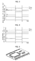
- Fig. 3 is a graph for showing the operation, in case when the power supply voltage "Vs" fluctuates or changes largely at the times “t1" and “t2”, with showing the time on the horizontal axis, and the boost ratio "a", the DC voltage “Ed” and the power supply voltage “Vs” on the vertical axis thereof.
- boost ratio "a” and the DC voltage "Ed” are shown, combining the operations in case of the conventional art (only the boost ratio stabilization controller portion 50A) (shown by a dotted line) and also in case of the present invention, each other.
- the correction is executed on the boost ratio "a", so that the DC voltage is maintained at the limit value "Ed Lim1 ".
- the boost ratio "a” also turns back to a normal value (i.e., a setup value), and thereby maintaining a normal DC voltage.
- Fig. 4 is a graph for showing the operation, in case when the power supply voltage "Vs" changes largely at the times “t1" and “t2”, with showing the time on the horizontal axis and the boost ratio "a", the DC voltage "Ed” and the load “L” on the vertical axis thereof.
- the boost ratio "a” and the DC voltage "Ed” are also shown, as is similar to that shown in Fig. 3 , combining the operation in case of the conventional art (only the boost ratio stabilization controller portion 50A) (shown by a dotted line) and that in case of the present invention (shown by a solid line) with each other.
- the present example of the ways of using is a hybrid IC, applying the controller circuit 5 shown in Fig. 1 therein, and it is shown by an outlook view thereof.
- the shunt resistor 53 mentioned above is provided, not within the hybrid IC because of changing the parts and a countermeasure to noises, but within a space same for the power circuit parts, such as, the switching element 31, etc.
- the input/output terminals of the controller circuit 5 shown in Fig. 1 are three (3); i.e., an input current detector terminal, a DC voltage detector terminal and a drive signal output terminal, but other than those, with provision of a boost ratio setup terminal, a DC voltage limiter value setup terminal, a load condition information detector terminal for detecting the condition of the load connected with and functions thereof, therein, it is possible to obtain a hybrid IC, further increasing the flexibility thereof.
- Fig. 6 is a control block diagram of the present embodiment
- Figs. 7 and 8 are views for explaining the operations of the present embodiment. The entire circuit structures are same to those shown in Fig. 1 .
- Fig. 6 is constructed with, as similar to the embodiment 1, the boost ratio stabilization controller portion 50A relating to the conventional art and a boost ratio corrector portion 50C according to the present invention.
- the boost ratio corrector portion 50C has the structures similar to that of the boost ratio corrector portion 50B, which was explained in the embodiment 1, and an aspect differing therefrom lies in a limit value "Ed Lim2 " and a limiter 504. Further, a proportion/integration compensator 502 perform the operation same to that of the proportion/integration compensator 501 shown in Fig. 2 .
- the limiter 504 is so setup that it corrects the boost ratio "a" only when the DC voltage value comes down lower than the limit value "Ed Lim2 " (i.e., operating only into a direction of increasing the boost ratio).
- the view for explaining the operation shown in Fig. 7 similar to the first embodiment, showing the time on the horizontal axis, and the boost ratio "a", the DC voltage “Ed” and the power supply voltage “Vs” on the vertical axis thereof, shows the operation when the power supply voltage "Vs" fluctuates largely at the times "t1" and "t2".
- the boost ratio "a” and the DC voltage "Ed” are shown, combining the operations in case of the conventional art (only the boost ratio stabilization controller portion 50A) (shown by a dotted line) and also in case of the present invention, each other.
- Fig. 8 is a graph for showing the operation, in case when the power supply voltage "Vs" changes largely at the times “t1" and “t2”, with showing the time on the horizontal axis and the boost ratio "a", the DC voltage "Ed” and the load “L” on the vertical axis thereof.
- Fig. 9 is a view for showing the entire structures of a motor driver apparatus, according to the present invention
- Fig. 10 is a control block diagram for showing the contents of control
- Figs. 11 and 12 are views for explaining the operation of the present embodiment
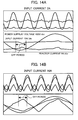
- Figs. 13A and 13B and 14A and 14B are views for showing the waveforms of input currents flowing into the power supply circuit
- Fig. 15 is an outlook view of a module, as an example of ways of using of the present embodiment.
- a motor driver circuit being made up with a motor 9 and an inverter circuit 8
- the controller circuit of the power supply circuit according to the present invention and the controller circuit of the inverter circuit 8 mentioned above are unified or built up as an unit, in the structures thereof.
- the controller circuit 7 shown in Fig. 9 uses a microcomputer therein, so that the power supply circuit and the inverter circuit are controlled by one (1) set of the microcomputer, in the structures thereof.
- the inverter circuit 8 is an inverter circuit, being made up with an IGBT and diodes, and the motor 9 is a permanent magnet synchronous motor.
- diodes 21 and 22 in the rectifier circuit 2 perform the operations similar to that of the diode 33 of the boost chopper circuit 3 of the first and second embodiments, other than the rectifying operation of the power supply.
- the above diodes 21 and 22 perform the two (2) operations mentioned above, and with adopting this circuit structure, there can be obtain an effect of reducing the loss for one (1) piece of diode.
- the controller circuit 7 controls the power supply circuit of the present invention and the inverter circuit with using the microcomputer, as was mentioned above, and within the microcomputer (i.e., a computing means 70) are conducted a computation for controlling the power supply circuit, which was explained in the first and second embodiment, and also a computation for controlling the inverter circuit.
- the power supply circuit executes the operation similar to that in the first and second embodiments.
- Fig. 11 shows the boost ratio "a” and the DC voltage "Ed” with respect to the load.
- the present embodiment as is shown in Fig. 10 , has such the structure of combining the controller structures explained in the first and second embodiments together, that the DC voltage changes between the limit value "Ed Lim1 " and the limit value "Ed Lim2 " in the operation thereof.
- the boost ratio corrector portion 50B when the load comes to a light load, being equal or less than the load "L1", then the boost ratio corrector portion 50B operates, so that the boost ratio "a” is corrected (i.e., decreased) and the DC voltage is controlled at the limit value "Ed Lim1 ".
- the boost ratio corrector portion 50C operates, so that the boost ratio "a” is corrected (i.e., increased) and the DC voltage is controlled at the limit value "Ed Lim2 ".
- Fig. 12 shows the boost ratio "a” and the DC voltage "Ed” with respect to the power supply voltage, wherein since moving of the boost ratio "a” and the DC voltage "Ed” is similar to that shown in Fig. 11 , then the explanation thereof will be omitted.
- Figs. 13A and 13B and Figs. 14A and 14B show the waveforms, as results of experiments, of the input current (or a reactor current), flowing into the power supply circuit, and the power supply voltage, when changing the load while keeping the power supply voltage to be constant.
- Figs. 13A and 13B show the results of experiments in the case of applying the conventional art (i.e., only the boost ratio stabilization controller portion 50A), and Figs. 14A and 14B in the case of applying the present invention.
- Both Figs. 13A and 14A show the results when the input current is "2A”
- Figs. 13B and 14B show the results when the input current is "16A”, respectively.
- Also, in addition thereto is shown a switching OFF period under the partial switching operation.
- the input current with applying the present invention therein has the waveform, as shown in Figs. 14A and 14B , changing the switching OFF period (reduced by about 15%) and less in the distortion ratio.
- the value of the harmonic current is not shown in the figure, but with the waveform shown in Fig. 14B , the harmonic current value is also decreased.
- Fig. 15 is an outlook view of a module of unifying the power supply circuit, the inverter circuit and the controller circuit, as an example of the ways of applying the present embodiment therein.
- the present module is a one-body module of disposing power system semiconductors, such as, the IGBT and the diodes, in a lower portion, mounting them in the form of bear chips, while disposing the controller circuit on a circuit board within an upper portion thereof. Building up them in the form of the module enables to apply the present invention, easily, and to construct a cheap system from a viewpoint of costs.
- the present embodiment was explained as the inverter circuit applying the vector control therein, but the similar effect can be obtained with using a 120-degree control-type inverter, which is widely used conventionally.
- the load condition information may be a value, which varies depending on the condition of the load, such as, a motor rotation speed, the input current, the DC current, the DC voltage, a DC power, a pulsating width of DC voltage, an input electric power, a torque, a peak value ratio of the inverter circuit, or the inverter duty ratio, etc., for example. Or, two (2) pieces or more of the values may be used in common.
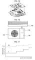
- Fig. 16 is an outlook view of an inverter air conditioner, in case when applying the motor driver apparatus, which was explained in the third embodiment, into a motor driver apparatus for use in driving of a compressor of the inverter air conditioner
- Fig. 17 is a view for explaining the operation when the boost ratio "a" changes depending on the load (i.e., the rotation speed) of the inverter air conditioner.
- the boost ratio "a" is corrected when the DC voltage comes to be equal or higher than, or to be equal or lower than the limit value; however for achieving the compatibility between further increase of the efficiency and the high output, there is a necessity for changing the setup value of the boost ratio "a", by itself, depending on the load (i.e., the rotation speed) of the inverter.
- Fig. 16 shows an outlook view of the inverter air conditioner ofseparate-type,being constructed with an outdoor or exterior machine 600 and an indoor or interior machine 400.
- a compressor 300 unified with the motor and/or an exterior fan 100, and a compressor 300 and/or a motor driver apparatus 200 for driving the exterior fan 100.
- the boost ratio "a” may be fixed, as was mentioned in the previous embodiment, however by taking further increase of efficiency and/or stability of the motor control and high output into the consideration thereof, the boost ratio "a” is changed depending on the load condition.
- Fig. 17 is shown a motor rotation speed on the horizontal axis while the boost ratio "a" and the DC voltage "Ed” on the vertical axis thereof.
- the operation is made with lowering the boost ratio "a” within a region where the rotation speed of the motor is low, in other words, under the condition that the load is light.
- the switching loss or the like of the power supply circuit is decreased, and further it is also possible to reduce the losses of the inverter circuit and the motor, thereby enabling the operation at the high efficiency.
- the boost ratio "a” is changed in a step-wise manner depending on the motor rotation speed, but in an actual operation, there is a necessity for providing a hysteresis therein (illustration thereof is omitted). Also, the boost ratio "a” may be changed linearly, for may be changed with applying a certain function. Further, it is also possible to control the rotation speed with using the boost ratio "a”. In other words, it is possible to control the rotation speed of the motor with variable DC voltage by chaining the boost ratio "a".
- the load condition information may be a value changing depending on the condition of the load, such as, the motor rotation speed, the input current, the DC current, the DC voltage, the DC power, the pulsating width of DC voltage, the input electric power, the torque, the peak value ratio of the inverter circuit, or the inverter duty ratio, etc., for example. Or, two (2) pieces or more of the values may be used in common.
- boost ratio "a" which is determined depending on the load of the inverter air conditioner
Landscapes
- Engineering & Computer Science (AREA)
- Power Engineering (AREA)
- Physics & Mathematics (AREA)
- Mechanical Engineering (AREA)
- Thermal Sciences (AREA)
- General Engineering & Computer Science (AREA)
- Rectifiers (AREA)
- Dc-Dc Converters (AREA)
- Inverter Devices (AREA)
- Power Conversion In General (AREA)
- Control Of Ac Motors In General (AREA)
Applications Claiming Priority (1)
| Application Number | Priority Date | Filing Date | Title |
|---|---|---|---|
| JP2008047029A JP4500857B2 (ja) | 2008-02-28 | 2008-02-28 | 電源回路及び、それを用いたモータ駆動装置,空調機 |
Publications (2)
| Publication Number | Publication Date |
|---|---|
| EP2096742A1 true EP2096742A1 (de) | 2009-09-02 |
| EP2096742B1 EP2096742B1 (de) | 2018-08-01 |
Family
ID=40602260
Family Applications (1)
| Application Number | Title | Priority Date | Filing Date |
|---|---|---|---|
| EP09001897.9A Active EP2096742B1 (de) | 2008-02-28 | 2009-02-11 | Leistungsfaktorkorrekturschaltung für eine Klimaanlage |
Country Status (5)
| Country | Link |
|---|---|
| EP (1) | EP2096742B1 (de) |
| JP (1) | JP4500857B2 (de) |
| KR (1) | KR101129100B1 (de) |
| CN (2) | CN102801316B (de) |
| ES (1) | ES2694030T3 (de) |
Cited By (2)
| Publication number | Priority date | Publication date | Assignee | Title |
|---|---|---|---|---|
| CN116465055A (zh) * | 2023-03-21 | 2023-07-21 | 青岛海尔空调电子有限公司 | 空调及空调的控制方法 |
| CN120034079A (zh) * | 2025-02-05 | 2025-05-23 | 民华微(上海)电子科技有限公司 | 一种电机转速的控制方法 |
Families Citing this family (14)
| Publication number | Priority date | Publication date | Assignee | Title |
|---|---|---|---|---|
| JP5066168B2 (ja) * | 2009-12-11 | 2012-11-07 | 株式会社日立製作所 | 電源回路及びそれを用いたモータ駆動装置並びに冷凍機器 |
| CN102783007B (zh) * | 2010-03-31 | 2015-08-05 | 日立空调·家用电器株式会社 | 转换器装置、马达驱动用模块以及冷冻机 |
| JP5922869B2 (ja) * | 2011-01-18 | 2016-05-24 | ダイキン工業株式会社 | 電力変換装置 |
| JP5675567B2 (ja) * | 2011-11-30 | 2015-02-25 | 日立アプライアンス株式会社 | 電力変換装置、電動機駆動装置及び空気調和機 |
| CN103248258B (zh) * | 2012-02-10 | 2015-07-08 | 美固电子(深圳)有限公司 | 正弦波车载逆变器的逆变控制电路及正弦波车载逆变器 |
| CN102801335A (zh) * | 2012-08-17 | 2012-11-28 | 绍兴文理学院 | 一种稠油电热采加热电源 |
| CN104236009B (zh) * | 2013-06-20 | 2017-03-15 | 广东美的制冷设备有限公司 | 空调信号采集补偿装置和方法 |
| CN103795039B (zh) * | 2014-02-14 | 2017-01-25 | 苏州佳世达电通有限公司 | 电源转换器及其电容保护装置 |
| JP6597362B2 (ja) * | 2016-02-12 | 2019-10-30 | 株式会社デンソー | 電子制御ユニット、および、これを用いた電動パワーステアリング装置 |
| JP6354801B2 (ja) * | 2016-07-21 | 2018-07-11 | トヨタ自動車株式会社 | 昇圧コンバータ |
| KR101888842B1 (ko) * | 2017-01-02 | 2018-08-16 | 엘지전자 주식회사 | 모터 제어 장치 및 모터 제어 장치의 제어 방법 |
| CN113452269B (zh) * | 2021-04-20 | 2022-07-26 | 成都芯源系统有限公司 | 开关电源电路及方法 |
| CN114216244B (zh) * | 2021-11-29 | 2022-11-25 | 珠海格力电器股份有限公司 | 压缩机母线电压调整方法、装置和压缩机 |
| CN114448251B (zh) * | 2022-01-11 | 2023-06-23 | 四川大学 | 一种数字控制谐波补偿电路 |
Citations (5)
| Publication number | Priority date | Publication date | Assignee | Title |
|---|---|---|---|---|
| JPH01114372A (ja) * | 1987-10-28 | 1989-05-08 | Hitachi Ltd | 電源装置 |
| JPH02261059A (ja) * | 1989-03-29 | 1990-10-23 | Hitachi Ltd | 直流電圧脈動補正電源装置および電動機制御装置 |
| JPH03230759A (ja) * | 1990-02-02 | 1991-10-14 | Hitachi Ltd | 電源装置および力率改善方法 |
| JPH1141980A (ja) * | 1997-07-11 | 1999-02-12 | Hitachi Ltd | 電動機駆動装置及びこれを用いた空気調和機 |
| EP1919064A2 (de) * | 2006-10-31 | 2008-05-07 | Hitachi, Ltd. | Stromversorgungsschaltung und Steuerung dafür |
Family Cites Families (3)
| Publication number | Priority date | Publication date | Assignee | Title |
|---|---|---|---|---|
| US6075328A (en) * | 1996-10-18 | 2000-06-13 | Hitachi, Ltd. | PWM/PAM control mode switching type motor control apparatus, and motor drive and air-conditioner using the same |
| JP4304122B2 (ja) * | 2004-05-25 | 2009-07-29 | 三菱電機株式会社 | 電気車制御装置 |
| JP4468840B2 (ja) * | 2005-02-25 | 2010-05-26 | 三菱電機株式会社 | 電力変換装置 |
-
2008
- 2008-02-28 JP JP2008047029A patent/JP4500857B2/ja active Active
-
2009
- 2009-02-11 EP EP09001897.9A patent/EP2096742B1/de active Active
- 2009-02-11 ES ES09001897.9T patent/ES2694030T3/es active Active
- 2009-02-19 CN CN201210277447.4A patent/CN102801316B/zh active Active
- 2009-02-19 KR KR1020090014100A patent/KR101129100B1/ko active Active
- 2009-02-19 CN CN200910008001XA patent/CN101521469B/zh active Active
Patent Citations (5)
| Publication number | Priority date | Publication date | Assignee | Title |
|---|---|---|---|---|
| JPH01114372A (ja) * | 1987-10-28 | 1989-05-08 | Hitachi Ltd | 電源装置 |
| JPH02261059A (ja) * | 1989-03-29 | 1990-10-23 | Hitachi Ltd | 直流電圧脈動補正電源装置および電動機制御装置 |
| JPH03230759A (ja) * | 1990-02-02 | 1991-10-14 | Hitachi Ltd | 電源装置および力率改善方法 |
| JPH1141980A (ja) * | 1997-07-11 | 1999-02-12 | Hitachi Ltd | 電動機駆動装置及びこれを用いた空気調和機 |
| EP1919064A2 (de) * | 2006-10-31 | 2008-05-07 | Hitachi, Ltd. | Stromversorgungsschaltung und Steuerung dafür |
Cited By (2)
| Publication number | Priority date | Publication date | Assignee | Title |
|---|---|---|---|---|
| CN116465055A (zh) * | 2023-03-21 | 2023-07-21 | 青岛海尔空调电子有限公司 | 空调及空调的控制方法 |
| CN120034079A (zh) * | 2025-02-05 | 2025-05-23 | 民华微(上海)电子科技有限公司 | 一种电机转速的控制方法 |
Also Published As
| Publication number | Publication date |
|---|---|
| KR101129100B1 (ko) | 2012-03-23 |
| JP2009207282A (ja) | 2009-09-10 |
| EP2096742B1 (de) | 2018-08-01 |
| CN102801316B (zh) | 2015-03-25 |
| JP4500857B2 (ja) | 2010-07-14 |
| ES2694030T3 (es) | 2018-12-17 |
| CN101521469B (zh) | 2013-12-25 |
| KR20090093820A (ko) | 2009-09-02 |
| CN101521469A (zh) | 2009-09-02 |
| CN102801316A (zh) | 2012-11-28 |
Similar Documents
| Publication | Publication Date | Title |
|---|---|---|
| EP2096742B1 (de) | Leistungsfaktorkorrekturschaltung für eine Klimaanlage | |
| CN101174794B (zh) | 电源电路及其中使用的控制电路 | |
| US9054586B2 (en) | Methods and apparatus for continuous and discontinuous active rectifier boost operation to increase power converter rating | |
| KR101408107B1 (ko) | 컨버터 장치, 모터 구동용 모듈, 및 냉동 기기 | |
| EP2333943B1 (de) | Netzstromkreis, Motorantriebsvorrichtung und Kühl- und Klimaanlage | |
| US8988024B2 (en) | Method and control system for driving a brushless electric motor | |
| CN103580469B (zh) | 一种用于永磁同步电机的功率因数校正方法 | |
| EP2099116A2 (de) | Motorantrieb mit Umrichterschaltung | |
| US11362603B2 (en) | Capacitance reductions | |
| JP5286309B2 (ja) | 電源回路およびその制御回路 | |
| JP3475727B2 (ja) | インバータ装置およびインバータ制御システム装置 | |
| EP3021479B1 (de) | Vorrichtung zur steuerung eines umrichters | |
| WO2025069183A1 (ja) | 電力変換装置、電動機駆動装置及び冷凍サイクル適用機器 | |
| JP7490089B2 (ja) | 空気調和機 | |
| JPH0265667A (ja) | コンバータの制御装置 | |
| JPH0568375A (ja) | 空気調和機の制御方法 | |
| Bao et al. | A variable frequency speed control system based on single-phase input without electrolytic capacitor | |
| JP2008263693A (ja) | 1ピストンロータリーコンプレッサの制御装置 | |
| JP2000230752A (ja) | 空気調和機の制御装置 |
Legal Events
| Date | Code | Title | Description |
|---|---|---|---|
| PUAI | Public reference made under article 153(3) epc to a published international application that has entered the european phase |
Free format text: ORIGINAL CODE: 0009012 |
|
| 17P | Request for examination filed |
Effective date: 20090211 |
|
| AK | Designated contracting states |
Kind code of ref document: A1 Designated state(s): AT BE BG CH CY CZ DE DK EE ES FI FR GB GR HR HU IE IS IT LI LT LU LV MC MK MT NL NO PL PT RO SE SI SK TR |
|
| AX | Request for extension of the european patent |
Extension state: AL BA RS |
|
| AKX | Designation fees paid |
Designated state(s): AT BE BG CH CY CZ DE DK EE ES FI FR GB GR HR HU IE IS IT LI LT LU LV MC MK MT NL NO PL PT RO SE SI SK TR |
|
| 17Q | First examination report despatched |
Effective date: 20161006 |
|
| STAA | Information on the status of an ep patent application or granted ep patent |
Free format text: STATUS: EXAMINATION IS IN PROGRESS |
|
| GRAP | Despatch of communication of intention to grant a patent |
Free format text: ORIGINAL CODE: EPIDOSNIGR1 |
|
| STAA | Information on the status of an ep patent application or granted ep patent |
Free format text: STATUS: GRANT OF PATENT IS INTENDED |
|
| INTG | Intention to grant announced |
Effective date: 20180212 |
|
| GRAS | Grant fee paid |
Free format text: ORIGINAL CODE: EPIDOSNIGR3 |
|
| GRAA | (expected) grant |
Free format text: ORIGINAL CODE: 0009210 |
|
| STAA | Information on the status of an ep patent application or granted ep patent |
Free format text: STATUS: THE PATENT HAS BEEN GRANTED |
|
| AK | Designated contracting states |
Kind code of ref document: B1 Designated state(s): AT BE BG CH CY CZ DE DK EE ES FI FR GB GR HR HU IE IS IT LI LT LU LV MC MK MT NL NO PL PT RO SE SI SK TR |
|
| REG | Reference to a national code |
Ref country code: GB Ref legal event code: FG4D |
|
| REG | Reference to a national code |
Ref country code: CH Ref legal event code: EP Ref country code: AT Ref legal event code: REF Ref document number: 1025510 Country of ref document: AT Kind code of ref document: T Effective date: 20180815 |
|
| REG | Reference to a national code |
Ref country code: IE Ref legal event code: FG4D |
|
| REG | Reference to a national code |
Ref country code: DE Ref legal event code: R096 Ref document number: 602009053530 Country of ref document: DE |
|
| REG | Reference to a national code |
Ref country code: NL Ref legal event code: MP Effective date: 20180801 |
|
| REG | Reference to a national code |
Ref country code: ES Ref legal event code: FG2A Ref document number: 2694030 Country of ref document: ES Kind code of ref document: T3 Effective date: 20181217 |
|
| REG | Reference to a national code |
Ref country code: LT Ref legal event code: MG4D |
|
| REG | Reference to a national code |
Ref country code: AT Ref legal event code: MK05 Ref document number: 1025510 Country of ref document: AT Kind code of ref document: T Effective date: 20180801 |
|
| PG25 | Lapsed in a contracting state [announced via postgrant information from national office to epo] |
Ref country code: FI Free format text: LAPSE BECAUSE OF FAILURE TO SUBMIT A TRANSLATION OF THE DESCRIPTION OR TO PAY THE FEE WITHIN THE PRESCRIBED TIME-LIMIT Effective date: 20180801 Ref country code: LT Free format text: LAPSE BECAUSE OF FAILURE TO SUBMIT A TRANSLATION OF THE DESCRIPTION OR TO PAY THE FEE WITHIN THE PRESCRIBED TIME-LIMIT Effective date: 20180801 Ref country code: PL Free format text: LAPSE BECAUSE OF FAILURE TO SUBMIT A TRANSLATION OF THE DESCRIPTION OR TO PAY THE FEE WITHIN THE PRESCRIBED TIME-LIMIT Effective date: 20180801 Ref country code: BG Free format text: LAPSE BECAUSE OF FAILURE TO SUBMIT A TRANSLATION OF THE DESCRIPTION OR TO PAY THE FEE WITHIN THE PRESCRIBED TIME-LIMIT Effective date: 20181101 Ref country code: AT Free format text: LAPSE BECAUSE OF FAILURE TO SUBMIT A TRANSLATION OF THE DESCRIPTION OR TO PAY THE FEE WITHIN THE PRESCRIBED TIME-LIMIT Effective date: 20180801 Ref country code: SE Free format text: LAPSE BECAUSE OF FAILURE TO SUBMIT A TRANSLATION OF THE DESCRIPTION OR TO PAY THE FEE WITHIN THE PRESCRIBED TIME-LIMIT Effective date: 20180801 Ref country code: GR Free format text: LAPSE BECAUSE OF FAILURE TO SUBMIT A TRANSLATION OF THE DESCRIPTION OR TO PAY THE FEE WITHIN THE PRESCRIBED TIME-LIMIT Effective date: 20181102 Ref country code: NL Free format text: LAPSE BECAUSE OF FAILURE TO SUBMIT A TRANSLATION OF THE DESCRIPTION OR TO PAY THE FEE WITHIN THE PRESCRIBED TIME-LIMIT Effective date: 20180801 Ref country code: NO Free format text: LAPSE BECAUSE OF FAILURE TO SUBMIT A TRANSLATION OF THE DESCRIPTION OR TO PAY THE FEE WITHIN THE PRESCRIBED TIME-LIMIT Effective date: 20181101 Ref country code: IS Free format text: LAPSE BECAUSE OF FAILURE TO SUBMIT A TRANSLATION OF THE DESCRIPTION OR TO PAY THE FEE WITHIN THE PRESCRIBED TIME-LIMIT Effective date: 20181201 |
|
| PG25 | Lapsed in a contracting state [announced via postgrant information from national office to epo] |
Ref country code: LV Free format text: LAPSE BECAUSE OF FAILURE TO SUBMIT A TRANSLATION OF THE DESCRIPTION OR TO PAY THE FEE WITHIN THE PRESCRIBED TIME-LIMIT Effective date: 20180801 Ref country code: HR Free format text: LAPSE BECAUSE OF FAILURE TO SUBMIT A TRANSLATION OF THE DESCRIPTION OR TO PAY THE FEE WITHIN THE PRESCRIBED TIME-LIMIT Effective date: 20180801 |
|
| PG25 | Lapsed in a contracting state [announced via postgrant information from national office to epo] |
Ref country code: CZ Free format text: LAPSE BECAUSE OF FAILURE TO SUBMIT A TRANSLATION OF THE DESCRIPTION OR TO PAY THE FEE WITHIN THE PRESCRIBED TIME-LIMIT Effective date: 20180801 Ref country code: EE Free format text: LAPSE BECAUSE OF FAILURE TO SUBMIT A TRANSLATION OF THE DESCRIPTION OR TO PAY THE FEE WITHIN THE PRESCRIBED TIME-LIMIT Effective date: 20180801 Ref country code: RO Free format text: LAPSE BECAUSE OF FAILURE TO SUBMIT A TRANSLATION OF THE DESCRIPTION OR TO PAY THE FEE WITHIN THE PRESCRIBED TIME-LIMIT Effective date: 20180801 |
|
| REG | Reference to a national code |
Ref country code: DE Ref legal event code: R097 Ref document number: 602009053530 Country of ref document: DE |
|
| PG25 | Lapsed in a contracting state [announced via postgrant information from national office to epo] |
Ref country code: DK Free format text: LAPSE BECAUSE OF FAILURE TO SUBMIT A TRANSLATION OF THE DESCRIPTION OR TO PAY THE FEE WITHIN THE PRESCRIBED TIME-LIMIT Effective date: 20180801 Ref country code: SK Free format text: LAPSE BECAUSE OF FAILURE TO SUBMIT A TRANSLATION OF THE DESCRIPTION OR TO PAY THE FEE WITHIN THE PRESCRIBED TIME-LIMIT Effective date: 20180801 |
|
| PLBE | No opposition filed within time limit |
Free format text: ORIGINAL CODE: 0009261 |
|
| STAA | Information on the status of an ep patent application or granted ep patent |
Free format text: STATUS: NO OPPOSITION FILED WITHIN TIME LIMIT |
|
| 26N | No opposition filed |
Effective date: 20190503 |
|
| PG25 | Lapsed in a contracting state [announced via postgrant information from national office to epo] |
Ref country code: SI Free format text: LAPSE BECAUSE OF FAILURE TO SUBMIT A TRANSLATION OF THE DESCRIPTION OR TO PAY THE FEE WITHIN THE PRESCRIBED TIME-LIMIT Effective date: 20180801 |
|
| REG | Reference to a national code |
Ref country code: DE Ref legal event code: R119 Ref document number: 602009053530 Country of ref document: DE |
|
| REG | Reference to a national code |
Ref country code: CH Ref legal event code: PL |
|
| PG25 | Lapsed in a contracting state [announced via postgrant information from national office to epo] |
Ref country code: LU Free format text: LAPSE BECAUSE OF NON-PAYMENT OF DUE FEES Effective date: 20190211 Ref country code: MC Free format text: LAPSE BECAUSE OF FAILURE TO SUBMIT A TRANSLATION OF THE DESCRIPTION OR TO PAY THE FEE WITHIN THE PRESCRIBED TIME-LIMIT Effective date: 20180801 |
|
| REG | Reference to a national code |
Ref country code: BE Ref legal event code: MM Effective date: 20190228 |
|
| REG | Reference to a national code |
Ref country code: IE Ref legal event code: MM4A |
|
| REG | Reference to a national code |
Ref country code: ES Ref legal event code: PC2A Owner name: HITACHI GLOBAL LIFE SOLUTIONS, INC. Effective date: 20191205 |
|
| PG25 | Lapsed in a contracting state [announced via postgrant information from national office to epo] |
Ref country code: LI Free format text: LAPSE BECAUSE OF NON-PAYMENT OF DUE FEES Effective date: 20190228 Ref country code: CH Free format text: LAPSE BECAUSE OF NON-PAYMENT OF DUE FEES Effective date: 20190228 |
|
| PG25 | Lapsed in a contracting state [announced via postgrant information from national office to epo] |
Ref country code: DE Free format text: LAPSE BECAUSE OF NON-PAYMENT OF DUE FEES Effective date: 20190903 Ref country code: IE Free format text: LAPSE BECAUSE OF NON-PAYMENT OF DUE FEES Effective date: 20190211 |
|
| PG25 | Lapsed in a contracting state [announced via postgrant information from national office to epo] |
Ref country code: BE Free format text: LAPSE BECAUSE OF NON-PAYMENT OF DUE FEES Effective date: 20190228 |
|
| PG25 | Lapsed in a contracting state [announced via postgrant information from national office to epo] |
Ref country code: TR Free format text: LAPSE BECAUSE OF FAILURE TO SUBMIT A TRANSLATION OF THE DESCRIPTION OR TO PAY THE FEE WITHIN THE PRESCRIBED TIME-LIMIT Effective date: 20180801 |
|
| PG25 | Lapsed in a contracting state [announced via postgrant information from national office to epo] |
Ref country code: PT Free format text: LAPSE BECAUSE OF FAILURE TO SUBMIT A TRANSLATION OF THE DESCRIPTION OR TO PAY THE FEE WITHIN THE PRESCRIBED TIME-LIMIT Effective date: 20181201 Ref country code: MT Free format text: LAPSE BECAUSE OF NON-PAYMENT OF DUE FEES Effective date: 20190211 |
|
| PG25 | Lapsed in a contracting state [announced via postgrant information from national office to epo] |
Ref country code: CY Free format text: LAPSE BECAUSE OF FAILURE TO SUBMIT A TRANSLATION OF THE DESCRIPTION OR TO PAY THE FEE WITHIN THE PRESCRIBED TIME-LIMIT Effective date: 20180801 |
|
| PG25 | Lapsed in a contracting state [announced via postgrant information from national office to epo] |
Ref country code: HU Free format text: LAPSE BECAUSE OF FAILURE TO SUBMIT A TRANSLATION OF THE DESCRIPTION OR TO PAY THE FEE WITHIN THE PRESCRIBED TIME-LIMIT; INVALID AB INITIO Effective date: 20090211 |
|
| PG25 | Lapsed in a contracting state [announced via postgrant information from national office to epo] |
Ref country code: MK Free format text: LAPSE BECAUSE OF FAILURE TO SUBMIT A TRANSLATION OF THE DESCRIPTION OR TO PAY THE FEE WITHIN THE PRESCRIBED TIME-LIMIT Effective date: 20180801 |
|
| PGFP | Annual fee paid to national office [announced via postgrant information from national office to epo] |
Ref country code: GB Payment date: 20260121 Year of fee payment: 18 |
|
| PGFP | Annual fee paid to national office [announced via postgrant information from national office to epo] |
Ref country code: ES Payment date: 20260302 Year of fee payment: 18 |
|
| PGFP | Annual fee paid to national office [announced via postgrant information from national office to epo] |
Ref country code: IT Payment date: 20260121 Year of fee payment: 18 |
|
| PGFP | Annual fee paid to national office [announced via postgrant information from national office to epo] |
Ref country code: FR Payment date: 20260121 Year of fee payment: 18 |