EP2097725B1 - Ouverture de commande pour un détecteur ir - Google Patents
Ouverture de commande pour un détecteur ir Download PDFInfo
- Publication number
- EP2097725B1 EP2097725B1 EP07863227.0A EP07863227A EP2097725B1 EP 2097725 B1 EP2097725 B1 EP 2097725B1 EP 07863227 A EP07863227 A EP 07863227A EP 2097725 B1 EP2097725 B1 EP 2097725B1
- Authority
- EP
- European Patent Office
- Prior art keywords
- sensor
- base
- cap
- die
- aperture
- Prior art date
- Legal status (The legal status is an assumption and is not a legal conclusion. Google has not performed a legal analysis and makes no representation as to the accuracy of the status listed.)
- Not-in-force
Links
Images



Classifications
-
- G—PHYSICS
- G01—MEASURING; TESTING
- G01J—MEASUREMENT OF INTENSITY, VELOCITY, SPECTRAL CONTENT, POLARISATION, PHASE OR PULSE CHARACTERISTICS OF INFRARED, VISIBLE OR ULTRAVIOLET LIGHT; COLORIMETRY; RADIATION PYROMETRY
- G01J1/00—Photometry, e.g. photographic exposure meter
- G01J1/42—Photometry, e.g. photographic exposure meter using electric radiation detectors
- G01J1/4228—Photometry, e.g. photographic exposure meter using electric radiation detectors arrangements with two or more detectors, e.g. for sensitivity compensation
-
- G—PHYSICS
- G01—MEASURING; TESTING
- G01J—MEASUREMENT OF INTENSITY, VELOCITY, SPECTRAL CONTENT, POLARISATION, PHASE OR PULSE CHARACTERISTICS OF INFRARED, VISIBLE OR ULTRAVIOLET LIGHT; COLORIMETRY; RADIATION PYROMETRY
- G01J1/00—Photometry, e.g. photographic exposure meter
- G01J1/02—Details
- G01J1/04—Optical or mechanical part supplementary adjustable parts
-
- G—PHYSICS
- G01—MEASURING; TESTING
- G01J—MEASUREMENT OF INTENSITY, VELOCITY, SPECTRAL CONTENT, POLARISATION, PHASE OR PULSE CHARACTERISTICS OF INFRARED, VISIBLE OR ULTRAVIOLET LIGHT; COLORIMETRY; RADIATION PYROMETRY
- G01J1/00—Photometry, e.g. photographic exposure meter
- G01J1/02—Details
- G01J1/04—Optical or mechanical part supplementary adjustable parts
- G01J1/0407—Optical elements not provided otherwise, e.g. manifolds, windows, holograms, gratings
- G01J1/0462—Slit arrangements
-
- G—PHYSICS
- G01—MEASURING; TESTING
- G01J—MEASUREMENT OF INTENSITY, VELOCITY, SPECTRAL CONTENT, POLARISATION, PHASE OR PULSE CHARACTERISTICS OF INFRARED, VISIBLE OR ULTRAVIOLET LIGHT; COLORIMETRY; RADIATION PYROMETRY
- G01J1/00—Photometry, e.g. photographic exposure meter
- G01J1/02—Details
- G01J1/0204—Compact construction
-
- H—ELECTRICITY
- H10—SEMICONDUCTOR DEVICES; ELECTRIC SOLID-STATE DEVICES NOT OTHERWISE PROVIDED FOR
- H10W—GENERIC PACKAGES, INTERCONNECTIONS, CONNECTORS OR OTHER CONSTRUCTIONAL DETAILS OF DEVICES COVERED BY CLASS H10
- H10W72/00—Interconnections or connectors in packages
- H10W72/50—Bond wires
- H10W72/551—Materials of bond wires
- H10W72/552—Materials of bond wires comprising metals or metalloids, e.g. silver
- H10W72/5522—Materials of bond wires comprising metals or metalloids, e.g. silver comprising gold [Au]
-
- H—ELECTRICITY
- H10—SEMICONDUCTOR DEVICES; ELECTRIC SOLID-STATE DEVICES NOT OTHERWISE PROVIDED FOR
- H10W—GENERIC PACKAGES, INTERCONNECTIONS, CONNECTORS OR OTHER CONSTRUCTIONAL DETAILS OF DEVICES COVERED BY CLASS H10
- H10W72/00—Interconnections or connectors in packages
- H10W72/851—Dispositions of multiple connectors or interconnections
- H10W72/874—On different surfaces
- H10W72/884—Die-attach connectors and bond wires
-
- H—ELECTRICITY
- H10—SEMICONDUCTOR DEVICES; ELECTRIC SOLID-STATE DEVICES NOT OTHERWISE PROVIDED FOR
- H10W—GENERIC PACKAGES, INTERCONNECTIONS, CONNECTORS OR OTHER CONSTRUCTIONAL DETAILS OF DEVICES COVERED BY CLASS H10
- H10W74/00—Encapsulations, e.g. protective coatings
- H10W74/10—Encapsulations, e.g. protective coatings characterised by their shape or disposition
-
- H—ELECTRICITY
- H10—SEMICONDUCTOR DEVICES; ELECTRIC SOLID-STATE DEVICES NOT OTHERWISE PROVIDED FOR
- H10W—GENERIC PACKAGES, INTERCONNECTIONS, CONNECTORS OR OTHER CONSTRUCTIONAL DETAILS OF DEVICES COVERED BY CLASS H10
- H10W90/00—Package configurations
- H10W90/701—Package configurations characterised by the relative positions of pads or connectors relative to package parts
- H10W90/731—Package configurations characterised by the relative positions of pads or connectors relative to package parts of die-attach connectors
- H10W90/736—Package configurations characterised by the relative positions of pads or connectors relative to package parts of die-attach connectors between a chip and a stacked lead frame, conducting package substrate or heat sink
-
- H—ELECTRICITY
- H10—SEMICONDUCTOR DEVICES; ELECTRIC SOLID-STATE DEVICES NOT OTHERWISE PROVIDED FOR
- H10W—GENERIC PACKAGES, INTERCONNECTIONS, CONNECTORS OR OTHER CONSTRUCTIONAL DETAILS OF DEVICES COVERED BY CLASS H10
- H10W90/00—Package configurations
- H10W90/701—Package configurations characterised by the relative positions of pads or connectors relative to package parts
- H10W90/751—Package configurations characterised by the relative positions of pads or connectors relative to package parts of bond wires
- H10W90/756—Package configurations characterised by the relative positions of pads or connectors relative to package parts of bond wires between a chip and a stacked lead frame, conducting package substrate or heat sink
Definitions
- This invention relates to an improved, integral control aperture for an IR sensor.
- infra-red (IR) sensors employ a metal can containing a silicon chip containing the IR sensor. There is a hole in the can which defines the IR aperture and the hole is typically sealed with a silicon window transparent to IR wavelengths. These tend to be expensive, large and cumbersome units, which can suffer from alignment issues and are limited in the types of mountings with which they can be used.
- the invention results from the realization that an improved integral control aperture for an IR sensor which better controls the spot:distance ratio can be fabricated using existing structure, materials, and techniques. This can be achieved with an IR sensor mounted on a die and an IR opaque aperture layer on or proximate to the die having an IR transmissive aperture aligned with the IR sensor for controlling the field of view and focus of the IR sensor.
- This invention features a control aperture for an IR sensor including a die having a base and a cap, and an IR sensor disposed on the base.
- An IR opaque aperture layer on the die has an IR transmissive aperture aligned with the IR sensor for controlling the field of view and focus of the IR sensor.
- the IR may be on one side of the die and the aperture layer may be on the other and the die is transparent to IR.
- the aperture layer may include a paddle bonded to the die.
- the aperture layer may include a copper alloy material.
- the die includes a base supporting the IR sensor and a cap covering the IR sensor.
- the die and paddle may be mounted in a molded package.
- the die may include silicon.
- the aperture layer may include an IR opaque coating bonded to the die.
- the die may include solder bumps.
- the solder bumps may be on the side opposite the aperture layer.
- the aperture layer may be on the cap portion of the die covering the IR sensor on one side of the base of the die and the solder bumps may be on the other side of the die.
- the IR sensor may be on one side of the base of the die covered by the cap and the aperture layer may be on the other side of the die which contains solder bumps.
- the IR sensor may be on one side of the base of the die covered by the cap and the aperture layer may include a laminated layer bonded to the die on the other side from IR sensor.
- the laminate may carry solder bumps.
- the die may be disposed in a mold which together with the laminate layer forms a laminate package.
- the die may be disposed in a mold which constitutes the aperture layer on the cap portion of the die.
- the other side of the die is supported by a lead frame and the die is disposed in the mold which exposes at least a portion of the cap and the aperture layer may be disposed on the cap. There may be a coating on the other side of the die.
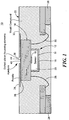
- FIG. 1 An exposed paddle lead frame package 10 including a silicon die 12 having a base 14 and cap portion 16.
- Cap 16 and base portion 14 may both be made of silicon.
- Cap 16 covers IR sensor 18 forming space or volume 20; volume 20 within cap 16 may be e.g. an air space or a vacuum.
- Silicon die 12 is mounted in a mold compound 22, such as Sumitomo G770, which also contains copper alloy component leads 24 and 26, interconnected with die 14 by means of gold bond wires 28 and 30.
- Silicon die 12 is placed on a lead frame paddle 34, typically fabricated from a copper alloy, which may be a prior art paddle. That paddle incorporates the control aperture 36. Initially such a paddle functions to support the silicon but here it does double service as the aperture layer.
- aperture 36 in aperture layer 34 is aligned with and on the other side of die 14 from sensor 18.
- Aperture layer or paddle 34 may be bonded to silicon die 12 by means of an adhesive 38 such as Ablestik 8290.
- a metalized layer 42 may be employed between die 12 and aperture layer 34.
- the metalized layer 42 will also be IR opaque as is the aperture layer 34 but in this case the aperture 44 in it may be more precisely deposited on the silicon 14, and etched for more accurate alignment with the sensor 18.
- This example can be employed in any exposed paddle lead frame package and provides the added benefit of some protection against handling damage for the etched focusing features 40 on the exposed silicon die 12.
- the etched silicon focusing elements are explained in greater detail in U.S. Patent Application 11/045,910, filed January 26, 2005 entitled SENSOR AND CAP ARRANGEMENT.
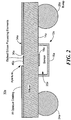
- a control aperture for an IR sensor on a bump part 10a, Fig. 2 uses aperture layer 34a, typically 5 - 25 microns thick which can be made of a filled organic polymer or could also be a metalized, typically sputtered, layer.
- the aperture layer is IR opaque and contains an aperture 36a, which is aligned with sensor 18a on the other side of die 12a on the die base 14a covered by die cap 16a.
- aperture 36a again there may etched silicon focusing elements 40a.
- Solder bumps 24a, 26a may be mechanically and electrically connected to die base 14a.
- solder bumps 24b and 26b may be mounted on a laminated layer 50, such as a printed circuit board, which is ported 52 to pass IR radiation 54.
- the aperture layer 34bb may be placed on the underside of die base 14b providing aperture 36bb in aperture layer 34bb and again there may be etched silicon focusing elements 40bb positioned there aligned with IR sensor 18b and aperture 36bb which is in turn aligned with port 52 in laminated layer 50.
- cap 16b has aperture layer 34b only on top and so the sidewalls 17b may allow some spurious IR radiation to reach sensor 18b. Coating processes such as dispensed coatings can deal with this if required.
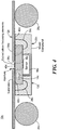
- a control aperture for an IR sensor may be used in a laminate package, 10c, Fig. 4 , where the aperture layer 34c may actually be a laminate board with conductor layers having an aperture 36c aligned with sensor 18c on the other side of die 12c covered by cap 16c.
- the die as well as gold wire bonds 28c and 30c are contained in a molded body 22c typically using the type of mold compound as cited before, e.g. Sumitomo G770. Silicon 14c may be adhered to the laminate aperture layer 34c by an adhesive 42c such as Ablestik 8290.
- the control aperture for an IR sensor of this example may also be practiced in a plastic package 10d, Fig.
- mold compound 22d also functions as the aperture layer 34d containing aperture 36d.
- a copper lead frame 60 which includes copper alloy component leads 24d, 26d.
- Silicon die 12d may be bonded to lead frame 60 by adhesive 42d, such as Ablestik 8290.
- plastic package 10e may be made with the mold 22e reduced to be more or less flush with the top of cap 16e so that an aperture layer 34e such as a metalized layer or a polymer is used having its own aperture 36e .
- an aperture layer 34e such as a metalized layer or a polymer is used having its own aperture 36e .
Landscapes
- Physics & Mathematics (AREA)
- General Physics & Mathematics (AREA)
- Spectroscopy & Molecular Physics (AREA)
- Solid State Image Pick-Up Elements (AREA)
- Automatic Focus Adjustment (AREA)
- Focusing (AREA)
Claims (8)
- Appareil détecteur IR comprenant :- un dé (12) ayant une base (14) et un couvercle (16), la base (14) ayant un premier côté et un second côté, dans lequel le second côté de la base (14) est soutenu par un cadre conducteur (60), et le couvercle (16) ayant une surface supérieure, le couvercle disposé sur le premier côté de la base, le couvercle et la base formant un vide et recouvrant un détecteur IR (18) disposé sur le premier côté de la base ;- une couche d'ouverture opaque aux IR (34) sur la surface supérieure du couvercle, la couche d'ouverture opaque aux IR ayant une couche transmettant les IR (36, 40) alignée avec ledit détecteur IR pour commander le champ de vision dudit détecteur IR ; dans lequel le dé est disposé dans un composé de moulage (22) à fleur avec la surface supérieure du couvercle, de telle manière que la couche d'ouverture opaque aux IR est en relief par rapport à la surface supérieure du composé de moulage ; et- des éléments de focalisation en silicium gravé (40) disposés sur la surface supérieure du couvercle à l'intérieur de la couche transmettant les IR, les éléments de focalisation en silicium gravé étant alignés avec le détecteur IR,dans lequel les premier et second côtés de la base sont sensiblement plats, de telle manière que le second côté de la base correspond à une surface adjacente du cadre conducteur sur toute la longueur de la base.
- Appareil détecteur IR selon la revendication 1, dans lequel le composé de moulage (22) expose au moins une partie du couvercle.
- Appareil détecteur IR selon la revendication 1, dans lequel ladite base (14) comprend du silicium.
- Appareil détecteur IR selon l'une quelconque des revendications précédentes, dans lequel la couche d'ouverture opaque aux IR est une couche métallisée.
- Appareil détecteur IR selon l'une quelconque des revendications 1 à 3, dans lequel la couche d'ouverture opaque aux IR est un polymère.
- Appareil détecteur IR selon l'une quelconque des revendications précédentes, dans lequel le cadre conducteur comporte des conducteurs en alliage de cuivre (24, 26) liés au dé par des liaisons en fil d'or (28, 30), les liaisons en fils étant contenues à l'intérieur du composé de moulage.
- Appareil détecteur IR selon l'une quelconque des revendications précédentes, dans lequel la base est liée au cadre conducteur par un adhésif.
- Appareil détecteur IR selon la revendication 7, dans lequel l'adhésif est de l'Ablestik 8290.
Applications Claiming Priority (2)
| Application Number | Priority Date | Filing Date | Title |
|---|---|---|---|
| US87730506P | 2006-12-27 | 2006-12-27 | |
| PCT/US2007/026253 WO2008085437A2 (fr) | 2006-12-27 | 2007-12-21 | Ouverture de commande pour un détecteur ir |
Publications (3)
| Publication Number | Publication Date |
|---|---|
| EP2097725A2 EP2097725A2 (fr) | 2009-09-09 |
| EP2097725A4 EP2097725A4 (fr) | 2012-06-06 |
| EP2097725B1 true EP2097725B1 (fr) | 2019-08-28 |
Family
ID=39593463
Family Applications (1)
| Application Number | Title | Priority Date | Filing Date |
|---|---|---|---|
| EP07863227.0A Not-in-force EP2097725B1 (fr) | 2006-12-27 | 2007-12-21 | Ouverture de commande pour un détecteur ir |
Country Status (3)
| Country | Link |
|---|---|
| US (1) | US8766186B2 (fr) |
| EP (1) | EP2097725B1 (fr) |
| WO (1) | WO2008085437A2 (fr) |
Families Citing this family (15)
| Publication number | Priority date | Publication date | Assignee | Title |
|---|---|---|---|---|
| US8487260B2 (en) * | 2005-01-26 | 2013-07-16 | Analog Devices, Inc. | Sensor |
| US7718967B2 (en) * | 2005-01-26 | 2010-05-18 | Analog Devices, Inc. | Die temperature sensors |
| US7807972B2 (en) * | 2005-01-26 | 2010-10-05 | Analog Devices, Inc. | Radiation sensor with cap and optical elements |
| US8523427B2 (en) | 2008-02-27 | 2013-09-03 | Analog Devices, Inc. | Sensor device with improved sensitivity to temperature variation in a semiconductor substrate |
| EP2264528A1 (fr) * | 2009-06-19 | 2010-12-22 | ASML Netherlands B.V. | Capteur et appareil lithographique |
| JP6097496B2 (ja) * | 2012-06-21 | 2017-03-15 | 旭化成エレクトロニクス株式会社 | 赤外線センサの製造方法 |
| US10884551B2 (en) | 2013-05-16 | 2021-01-05 | Analog Devices, Inc. | Integrated gesture sensor module |
| US9590129B2 (en) | 2014-11-19 | 2017-03-07 | Analog Devices Global | Optical sensor module |
| WO2018092795A1 (fr) * | 2016-11-15 | 2018-05-24 | パナソニックIpマネジメント株式会社 | Capteur infrarouge |
| WO2018166738A1 (fr) * | 2017-03-15 | 2018-09-20 | Asml Netherlands B.V. | Repère de capteur, et procédé de fabrication d'un repère de capteur |
| US20190206752A1 (en) * | 2017-12-29 | 2019-07-04 | Texas Instruments Incorporated | Integrated circuit packages with cavities and methods of manufacturing the same |
| US10712197B2 (en) | 2018-01-11 | 2020-07-14 | Analog Devices Global Unlimited Company | Optical sensor package |
| JP2019191340A (ja) * | 2018-04-24 | 2019-10-31 | Agc株式会社 | 遮光層付き透明板 |
| US10418294B1 (en) * | 2018-05-15 | 2019-09-17 | Texas Instruments Incorporated | Semiconductor device package with a cap to selectively exclude contact with mold compound |
| WO2019227065A1 (fr) * | 2018-05-24 | 2019-11-28 | Cvg Management Corporation | Mesure de température infrarouge et procédé de stabilisation associé |
Citations (2)
| Publication number | Priority date | Publication date | Assignee | Title |
|---|---|---|---|---|
| JP2001174323A (ja) * | 1999-12-17 | 2001-06-29 | Tdk Corp | 赤外線検出装置 |
| US20050081905A1 (en) * | 2003-10-17 | 2005-04-21 | Lan Alex H. | Thermopile IR detector package structure |
Family Cites Families (31)
| Publication number | Priority date | Publication date | Assignee | Title |
|---|---|---|---|---|
| US4760440A (en) * | 1983-10-31 | 1988-07-26 | General Electric Company | Package for solid state image sensors |
| US4994664A (en) * | 1989-03-27 | 1991-02-19 | Massachusetts Institute Of Technology | Optically coupled focal plane arrays using lenslets and multiplexers |
| JPH03210437A (ja) | 1989-11-02 | 1991-09-13 | Terumo Corp | 赤外線センサ及びその製造方法 |
| AU631734B2 (en) | 1990-04-18 | 1992-12-03 | Terumo Kabushiki Kaisha | Infrared ray sensor and method of manufacturing the same |
| JPH06249708A (ja) | 1993-02-23 | 1994-09-09 | Nissan Motor Co Ltd | 赤外線センサおよびその製造方法 |
| JPH07209089A (ja) * | 1994-01-24 | 1995-08-11 | Terumo Corp | 赤外線センサ |
| KR100186329B1 (ko) | 1996-06-14 | 1999-03-20 | 문정환 | 고체 촬상 소자용 반도체 패키지 |
| US5701008A (en) * | 1996-11-29 | 1997-12-23 | He Holdings, Inc. | Integrated infrared microlens and gas molecule getter grating in a vacuum package |
| US5869883A (en) | 1997-09-26 | 1999-02-09 | Stanley Wang, President Pantronix Corp. | Packaging of semiconductor circuit in pre-molded plastic package |
| JPH11132857A (ja) | 1997-10-28 | 1999-05-21 | Matsushita Electric Works Ltd | 赤外線検出器 |
| US6376769B1 (en) | 1999-05-18 | 2002-04-23 | Amerasia International Technology, Inc. | High-density electronic package, and method for making same |
| US6465786B1 (en) * | 1999-09-01 | 2002-10-15 | Micron Technology, Inc. | Deep infrared photodiode for a CMOS imager |
| CA2308000C (fr) | 2000-05-10 | 2004-01-06 | Ibm Canada Limited-Ibm Canada Limitee | Emetteur-recepteur infra-rouge pour transmission asymetrique de donnees |
| AUPR245701A0 (en) * | 2001-01-10 | 2001-02-01 | Silverbrook Research Pty Ltd | An apparatus (WSM10) |
| FR2819634B1 (fr) | 2001-01-15 | 2004-01-16 | St Microelectronics Sa | Boitier semi-conducteur a capteur, muni d'un insert et son procede de fabrication |
| US7518136B2 (en) * | 2001-12-17 | 2009-04-14 | Tecomet, Inc. | Devices, methods, and systems involving cast computed tomography collimators |
| US6844606B2 (en) * | 2002-02-04 | 2005-01-18 | Delphi Technologies, Inc. | Surface-mount package for an optical sensing device and method of manufacture |
| AU2002950739A0 (en) | 2002-08-13 | 2002-09-12 | The University Of Western Australia | A resonant cavity enhanced device and a method for fabricating same |
| US6879035B2 (en) | 2003-05-02 | 2005-04-12 | Athanasios J. Syllaios | Vacuum package fabrication of integrated circuit components |
| DE10327694A1 (de) | 2003-06-20 | 2005-01-05 | Robert Bosch Gmbh | Optische Sensoranordnung und entsprechendes Herstellungsverfahren |
| DE102004030418A1 (de) | 2004-06-24 | 2006-01-19 | Robert Bosch Gmbh | Mikrostrukturierter Infrarot-Sensor und ein Verfahren zu seiner Herstellung |
| DE102004031315A1 (de) | 2004-06-29 | 2006-01-19 | Robert Bosch Gmbh | Mikrostrukturierter Infrarot-Sensor |
| EP1626571A1 (fr) | 2004-08-13 | 2006-02-15 | STMicroelectronics Limited | Assemblage pour la formation d' images |
| US7294827B2 (en) * | 2004-09-21 | 2007-11-13 | Delphi Technologies, Inc. | Electronic module with light-blocking features |
| US7326932B2 (en) | 2005-01-26 | 2008-02-05 | Analog Devices, Inc. | Sensor and cap arrangement |
| US7329871B2 (en) * | 2005-02-04 | 2008-02-12 | Stc.Unm | Plasmonic enhanced infrared detector element |
| US7364945B2 (en) * | 2005-03-31 | 2008-04-29 | Stats Chippac Ltd. | Method of mounting an integrated circuit package in an encapsulant cavity |
| US20070108635A1 (en) * | 2005-04-28 | 2007-05-17 | Stats Chippac Ltd. | Integrated circuit package system |
| US7495325B2 (en) | 2005-05-05 | 2009-02-24 | Stats Chippac, Ltd. | Optical die-down quad flat non-leaded package |
| US7723146B2 (en) * | 2006-01-04 | 2010-05-25 | Stats Chippac Ltd. | Integrated circuit package system with image sensor system |
| US20070292982A1 (en) * | 2006-06-16 | 2007-12-20 | Jeffery Gail Holloway | Method for Manufacturing Transparent Windows in Molded Semiconductor Packages |
-
2007
- 2007-12-21 US US12/004,780 patent/US8766186B2/en active Active
- 2007-12-21 WO PCT/US2007/026253 patent/WO2008085437A2/fr not_active Ceased
- 2007-12-21 EP EP07863227.0A patent/EP2097725B1/fr not_active Not-in-force
Patent Citations (2)
| Publication number | Priority date | Publication date | Assignee | Title |
|---|---|---|---|---|
| JP2001174323A (ja) * | 1999-12-17 | 2001-06-29 | Tdk Corp | 赤外線検出装置 |
| US20050081905A1 (en) * | 2003-10-17 | 2005-04-21 | Lan Alex H. | Thermopile IR detector package structure |
Also Published As
| Publication number | Publication date |
|---|---|
| EP2097725A4 (fr) | 2012-06-06 |
| WO2008085437A2 (fr) | 2008-07-17 |
| EP2097725A2 (fr) | 2009-09-09 |
| US20080164415A1 (en) | 2008-07-10 |
| WO2008085437A3 (fr) | 2008-10-23 |
| US8766186B2 (en) | 2014-07-01 |
Similar Documents
| Publication | Publication Date | Title |
|---|---|---|
| EP2097725B1 (fr) | Ouverture de commande pour un détecteur ir | |
| US7566588B2 (en) | Semiconductor device with a resin-sealed optical semiconductor element | |
| EP1465244B1 (fr) | Boîtier de circuit intégré avec surfaces de puce exposées et fixation auxiliaire | |
| EP2373059B1 (fr) | Dispositif semi-conducteur et microphone | |
| US7673386B2 (en) | Flip-chip component production method | |
| KR101566597B1 (ko) | 케이스형 전기 소자 | |
| CN107566691B (zh) | 感光组件和摄像模组及其制造方法 | |
| US20080309805A1 (en) | Image sensor package | |
| CN110228786B (zh) | 半导体装置封装及其制造方法 | |
| KR20130113339A (ko) | 평면 형태를 가진 전기 소자 및 그 제조 방법 | |
| US20110267534A1 (en) | Image sensor package and camera module using same | |
| WO2021200406A1 (fr) | Dispositif à semi-conducteur | |
| US20120112368A1 (en) | Mems sensor package | |
| EP1806316B1 (fr) | Joint en polymère à cristaux liquides pour un dispositif MEMS | |
| US9576877B2 (en) | Electronic component, electronic device, method of manufacturing mounted member, and method of manufacturing electronic component | |
| KR20080087108A (ko) | 기판 구조 및 전자 기기 | |
| US7388192B2 (en) | Image sensing module and process for packaging the same | |
| WO2017134972A1 (fr) | Boîtier d'élément d'imagerie et dispositif d'imagerie | |
| CN111422817B (zh) | 传感器单元及将基板与载体互连的方法 | |
| CN111048468A (zh) | 电子元件的层叠件及其制造方法 | |
| US20100181636A1 (en) | Optical device, solid-state imaging device, and method of manufacturing optical device | |
| CN1979882A (zh) | 固态成像装置及其制造方法以及照相机模块 | |
| US20060273437A1 (en) | Optoelectronic semiconductor assembly with an optically transparent cover, and a method for producing optoelectronic semiconductor assembly with an optically transparent cover | |
| US7417327B2 (en) | IC chip package with cover | |
| CN114551604B (zh) | 芯片封装结构及其制造方法 |
Legal Events
| Date | Code | Title | Description |
|---|---|---|---|
| PUAI | Public reference made under article 153(3) epc to a published international application that has entered the european phase |
Free format text: ORIGINAL CODE: 0009012 |
|
| 17P | Request for examination filed |
Effective date: 20090624 |
|
| AK | Designated contracting states |
Kind code of ref document: A2 Designated state(s): AT BE BG CH CY CZ DE DK EE ES FI FR GB GR HU IE IS IT LI LT LU LV MC MT NL PL PT RO SE SI SK TR |
|
| RAP1 | Party data changed (applicant data changed or rights of an application transferred) |
Owner name: ANALOG DEVICES, INC. |
|
| DAX | Request for extension of the european patent (deleted) | ||
| A4 | Supplementary search report drawn up and despatched |
Effective date: 20120507 |
|
| RIC1 | Information provided on ipc code assigned before grant |
Ipc: G01J 1/42 20060101ALI20120501BHEP Ipc: G01J 5/00 20060101AFI20120501BHEP Ipc: G01J 1/04 20060101ALI20120501BHEP |
|
| 17Q | First examination report despatched |
Effective date: 20150507 |
|
| GRAP | Despatch of communication of intention to grant a patent |
Free format text: ORIGINAL CODE: EPIDOSNIGR1 |
|
| STAA | Information on the status of an ep patent application or granted ep patent |
Free format text: STATUS: GRANT OF PATENT IS INTENDED |
|
| INTG | Intention to grant announced |
Effective date: 20190329 |
|
| GRAS | Grant fee paid |
Free format text: ORIGINAL CODE: EPIDOSNIGR3 |
|
| GRAA | (expected) grant |
Free format text: ORIGINAL CODE: 0009210 |
|
| STAA | Information on the status of an ep patent application or granted ep patent |
Free format text: STATUS: THE PATENT HAS BEEN GRANTED |
|
| AK | Designated contracting states |
Kind code of ref document: B1 Designated state(s): AT BE BG CH CY CZ DE DK EE ES FI FR GB GR HU IE IS IT LI LT LU LV MC MT NL PL PT RO SE SI SK TR |
|
| REG | Reference to a national code |
Ref country code: GB Ref legal event code: FG4D |
|
| REG | Reference to a national code |
Ref country code: CH Ref legal event code: EP |
|
| REG | Reference to a national code |
Ref country code: AT Ref legal event code: REF Ref document number: 1172986 Country of ref document: AT Kind code of ref document: T Effective date: 20190915 |
|
| REG | Reference to a national code |
Ref country code: IE Ref legal event code: FG4D |
|
| REG | Reference to a national code |
Ref country code: DE Ref legal event code: R096 Ref document number: 602007059141 Country of ref document: DE |
|
| REG | Reference to a national code |
Ref country code: NL Ref legal event code: MP Effective date: 20190828 |
|
| REG | Reference to a national code |
Ref country code: LT Ref legal event code: MG4D |
|
| PG25 | Lapsed in a contracting state [announced via postgrant information from national office to epo] |
Ref country code: PT Free format text: LAPSE BECAUSE OF FAILURE TO SUBMIT A TRANSLATION OF THE DESCRIPTION OR TO PAY THE FEE WITHIN THE PRESCRIBED TIME-LIMIT Effective date: 20191230 Ref country code: FI Free format text: LAPSE BECAUSE OF FAILURE TO SUBMIT A TRANSLATION OF THE DESCRIPTION OR TO PAY THE FEE WITHIN THE PRESCRIBED TIME-LIMIT Effective date: 20190828 Ref country code: LT Free format text: LAPSE BECAUSE OF FAILURE TO SUBMIT A TRANSLATION OF THE DESCRIPTION OR TO PAY THE FEE WITHIN THE PRESCRIBED TIME-LIMIT Effective date: 20190828 Ref country code: NL Free format text: LAPSE BECAUSE OF FAILURE TO SUBMIT A TRANSLATION OF THE DESCRIPTION OR TO PAY THE FEE WITHIN THE PRESCRIBED TIME-LIMIT Effective date: 20190828 Ref country code: BG Free format text: LAPSE BECAUSE OF FAILURE TO SUBMIT A TRANSLATION OF THE DESCRIPTION OR TO PAY THE FEE WITHIN THE PRESCRIBED TIME-LIMIT Effective date: 20191128 Ref country code: SE Free format text: LAPSE BECAUSE OF FAILURE TO SUBMIT A TRANSLATION OF THE DESCRIPTION OR TO PAY THE FEE WITHIN THE PRESCRIBED TIME-LIMIT Effective date: 20190828 |
|
| PG25 | Lapsed in a contracting state [announced via postgrant information from national office to epo] |
Ref country code: IS Free format text: LAPSE BECAUSE OF FAILURE TO SUBMIT A TRANSLATION OF THE DESCRIPTION OR TO PAY THE FEE WITHIN THE PRESCRIBED TIME-LIMIT Effective date: 20191228 Ref country code: LV Free format text: LAPSE BECAUSE OF FAILURE TO SUBMIT A TRANSLATION OF THE DESCRIPTION OR TO PAY THE FEE WITHIN THE PRESCRIBED TIME-LIMIT Effective date: 20190828 Ref country code: GR Free format text: LAPSE BECAUSE OF FAILURE TO SUBMIT A TRANSLATION OF THE DESCRIPTION OR TO PAY THE FEE WITHIN THE PRESCRIBED TIME-LIMIT Effective date: 20191129 Ref country code: ES Free format text: LAPSE BECAUSE OF FAILURE TO SUBMIT A TRANSLATION OF THE DESCRIPTION OR TO PAY THE FEE WITHIN THE PRESCRIBED TIME-LIMIT Effective date: 20190828 |
|
| REG | Reference to a national code |
Ref country code: AT Ref legal event code: MK05 Ref document number: 1172986 Country of ref document: AT Kind code of ref document: T Effective date: 20190828 |
|
| PG25 | Lapsed in a contracting state [announced via postgrant information from national office to epo] |
Ref country code: TR Free format text: LAPSE BECAUSE OF FAILURE TO SUBMIT A TRANSLATION OF THE DESCRIPTION OR TO PAY THE FEE WITHIN THE PRESCRIBED TIME-LIMIT Effective date: 20190828 |
|
| PG25 | Lapsed in a contracting state [announced via postgrant information from national office to epo] |
Ref country code: DK Free format text: LAPSE BECAUSE OF FAILURE TO SUBMIT A TRANSLATION OF THE DESCRIPTION OR TO PAY THE FEE WITHIN THE PRESCRIBED TIME-LIMIT Effective date: 20190828 Ref country code: AT Free format text: LAPSE BECAUSE OF FAILURE TO SUBMIT A TRANSLATION OF THE DESCRIPTION OR TO PAY THE FEE WITHIN THE PRESCRIBED TIME-LIMIT Effective date: 20190828 Ref country code: EE Free format text: LAPSE BECAUSE OF FAILURE TO SUBMIT A TRANSLATION OF THE DESCRIPTION OR TO PAY THE FEE WITHIN THE PRESCRIBED TIME-LIMIT Effective date: 20190828 Ref country code: PL Free format text: LAPSE BECAUSE OF FAILURE TO SUBMIT A TRANSLATION OF THE DESCRIPTION OR TO PAY THE FEE WITHIN THE PRESCRIBED TIME-LIMIT Effective date: 20190828 Ref country code: IT Free format text: LAPSE BECAUSE OF FAILURE TO SUBMIT A TRANSLATION OF THE DESCRIPTION OR TO PAY THE FEE WITHIN THE PRESCRIBED TIME-LIMIT Effective date: 20190828 Ref country code: RO Free format text: LAPSE BECAUSE OF FAILURE TO SUBMIT A TRANSLATION OF THE DESCRIPTION OR TO PAY THE FEE WITHIN THE PRESCRIBED TIME-LIMIT Effective date: 20190828 |
|
| PG25 | Lapsed in a contracting state [announced via postgrant information from national office to epo] |
Ref country code: CZ Free format text: LAPSE BECAUSE OF FAILURE TO SUBMIT A TRANSLATION OF THE DESCRIPTION OR TO PAY THE FEE WITHIN THE PRESCRIBED TIME-LIMIT Effective date: 20190828 Ref country code: IS Free format text: LAPSE BECAUSE OF FAILURE TO SUBMIT A TRANSLATION OF THE DESCRIPTION OR TO PAY THE FEE WITHIN THE PRESCRIBED TIME-LIMIT Effective date: 20200224 Ref country code: SK Free format text: LAPSE BECAUSE OF FAILURE TO SUBMIT A TRANSLATION OF THE DESCRIPTION OR TO PAY THE FEE WITHIN THE PRESCRIBED TIME-LIMIT Effective date: 20190828 |
|
| REG | Reference to a national code |
Ref country code: DE Ref legal event code: R097 Ref document number: 602007059141 Country of ref document: DE |
|
| PLBE | No opposition filed within time limit |
Free format text: ORIGINAL CODE: 0009261 |
|
| STAA | Information on the status of an ep patent application or granted ep patent |
Free format text: STATUS: NO OPPOSITION FILED WITHIN TIME LIMIT |
|
| PG2D | Information on lapse in contracting state deleted |
Ref country code: IS |
|
| REG | Reference to a national code |
Ref country code: CH Ref legal event code: PL |
|
| 26N | No opposition filed |
Effective date: 20200603 |
|
| REG | Reference to a national code |
Ref country code: BE Ref legal event code: MM Effective date: 20191231 |
|
| PG25 | Lapsed in a contracting state [announced via postgrant information from national office to epo] |
Ref country code: SI Free format text: LAPSE BECAUSE OF FAILURE TO SUBMIT A TRANSLATION OF THE DESCRIPTION OR TO PAY THE FEE WITHIN THE PRESCRIBED TIME-LIMIT Effective date: 20190828 Ref country code: MC Free format text: LAPSE BECAUSE OF FAILURE TO SUBMIT A TRANSLATION OF THE DESCRIPTION OR TO PAY THE FEE WITHIN THE PRESCRIBED TIME-LIMIT Effective date: 20190828 |
|
| PG25 | Lapsed in a contracting state [announced via postgrant information from national office to epo] |
Ref country code: LU Free format text: LAPSE BECAUSE OF NON-PAYMENT OF DUE FEES Effective date: 20191221 Ref country code: IE Free format text: LAPSE BECAUSE OF NON-PAYMENT OF DUE FEES Effective date: 20191221 |
|
| PG25 | Lapsed in a contracting state [announced via postgrant information from national office to epo] |
Ref country code: BE Free format text: LAPSE BECAUSE OF NON-PAYMENT OF DUE FEES Effective date: 20191231 Ref country code: CH Free format text: LAPSE BECAUSE OF NON-PAYMENT OF DUE FEES Effective date: 20191231 Ref country code: LI Free format text: LAPSE BECAUSE OF NON-PAYMENT OF DUE FEES Effective date: 20191231 |
|
| PG25 | Lapsed in a contracting state [announced via postgrant information from national office to epo] |
Ref country code: CY Free format text: LAPSE BECAUSE OF FAILURE TO SUBMIT A TRANSLATION OF THE DESCRIPTION OR TO PAY THE FEE WITHIN THE PRESCRIBED TIME-LIMIT Effective date: 20190828 |
|
| PG25 | Lapsed in a contracting state [announced via postgrant information from national office to epo] |
Ref country code: MT Free format text: LAPSE BECAUSE OF FAILURE TO SUBMIT A TRANSLATION OF THE DESCRIPTION OR TO PAY THE FEE WITHIN THE PRESCRIBED TIME-LIMIT Effective date: 20190828 Ref country code: HU Free format text: LAPSE BECAUSE OF FAILURE TO SUBMIT A TRANSLATION OF THE DESCRIPTION OR TO PAY THE FEE WITHIN THE PRESCRIBED TIME-LIMIT; INVALID AB INITIO Effective date: 20071221 |
|
| PGFP | Annual fee paid to national office [announced via postgrant information from national office to epo] |
Ref country code: DE Payment date: 20211117 Year of fee payment: 15 Ref country code: FR Payment date: 20211118 Year of fee payment: 15 Ref country code: GB Payment date: 20211118 Year of fee payment: 15 |
|
| REG | Reference to a national code |
Ref country code: DE Ref legal event code: R119 Ref document number: 602007059141 Country of ref document: DE |
|
| GBPC | Gb: european patent ceased through non-payment of renewal fee |
Effective date: 20221221 |
|
| PG25 | Lapsed in a contracting state [announced via postgrant information from national office to epo] |
Ref country code: GB Free format text: LAPSE BECAUSE OF NON-PAYMENT OF DUE FEES Effective date: 20221221 Ref country code: DE Free format text: LAPSE BECAUSE OF NON-PAYMENT OF DUE FEES Effective date: 20230701 |
|
| PG25 | Lapsed in a contracting state [announced via postgrant information from national office to epo] |
Ref country code: FR Free format text: LAPSE BECAUSE OF NON-PAYMENT OF DUE FEES Effective date: 20221231 |