EP2099129A1 - Oberflächenwellenbauelement - Google Patents
Oberflächenwellenbauelement Download PDFInfo
- Publication number
- EP2099129A1 EP2099129A1 EP07850538A EP07850538A EP2099129A1 EP 2099129 A1 EP2099129 A1 EP 2099129A1 EP 07850538 A EP07850538 A EP 07850538A EP 07850538 A EP07850538 A EP 07850538A EP 2099129 A1 EP2099129 A1 EP 2099129A1
- Authority
- EP
- European Patent Office
- Prior art keywords
- idt electrode
- acoustic wave
- surface acoustic
- normalized
- thickness
- Prior art date
- Legal status (The legal status is an assumption and is not a legal conclusion. Google has not performed a legal analysis and makes no representation as to the accuracy of the status listed.)
- Withdrawn
Links
Images


Classifications
-
- H—ELECTRICITY
- H03—ELECTRONIC CIRCUITRY
- H03H—IMPEDANCE NETWORKS, e.g. RESONANT CIRCUITS; RESONATORS
- H03H9/00—Networks comprising electromechanical or electro-acoustic elements; Electromechanical resonators
- H03H9/02—Details
- H03H9/125—Driving means, e.g. electrodes, coils
- H03H9/145—Driving means, e.g. electrodes, coils for networks using surface acoustic waves
-
- H—ELECTRICITY
- H03—ELECTRONIC CIRCUITRY
- H03H—IMPEDANCE NETWORKS, e.g. RESONANT CIRCUITS; RESONATORS
- H03H9/00—Networks comprising electromechanical or electro-acoustic elements; Electromechanical resonators
- H03H9/02—Details
- H03H9/02535—Details of surface acoustic wave devices
- H03H9/02543—Characteristics of substrate, e.g. cutting angles
- H03H9/02551—Characteristics of substrate, e.g. cutting angles of quartz substrates
-
- H—ELECTRICITY
- H03—ELECTRONIC CIRCUITRY
- H03H—IMPEDANCE NETWORKS, e.g. RESONANT CIRCUITS; RESONATORS
- H03H9/00—Networks comprising electromechanical or electro-acoustic elements; Electromechanical resonators
- H03H9/02—Details
- H03H9/02535—Details of surface acoustic wave devices
- H03H9/02543—Characteristics of substrate, e.g. cutting angles
- H03H9/02574—Characteristics of substrate, e.g. cutting angles of combined substrates, multilayered substrates, piezoelectrical layers on not-piezoelectrical substrate
-
- H—ELECTRICITY
- H03—ELECTRONIC CIRCUITRY
- H03H—IMPEDANCE NETWORKS, e.g. RESONANT CIRCUITS; RESONATORS
- H03H9/00—Networks comprising electromechanical or electro-acoustic elements; Electromechanical resonators
- H03H9/02—Details
- H03H9/02535—Details of surface acoustic wave devices
- H03H9/02818—Means for compensation or elimination of undesirable effects
- H03H9/02834—Means for compensation or elimination of undesirable effects of temperature influence
Definitions
- the present invention relates to a surface acoustic wave device used for a bandpass filter, a resonator, or the like, and more particularly relates to a surface acoustic wave device having the structure in which at least one IDT electrode and a piezoelectric film composed of ZnO are laminated on a piezoelectric substrate composed of quartz.
- Non-Patent Document 1 a small surface acoustic wave filter having the structure in which a ZnO film and quartz are laminated to each other has been disclosed.
- a transversal type surface acoustic wave filter has been disclosed in which at least one IDT electrode composed of Al is formed on a piezoelectric substrate composed of 27° Y-cut X-propagation quartz, and in which a piezoelectric film composed of ZnO is laminated so as to cover the IDT electrode.
- a thickness H/ ⁇ of the IDT electrode normalized by the wavelength of a surface acoustic wave is set to 0.02.
- a normalized thickness H/ ⁇ of the piezoelectric film composed of ZnO is set to 0.3, and accordingly, a 380-MHz bandpass filter in the IF stage of WCDMA mobile phones is formed.
- Non-Patent Document 1 As disclosed in Non-Patent Document 1, heretofore, a laminate structure of ZnO/IDT electrode/quartz has been studied for application to a transversal surface acoustic wave filter device.
- a surface acoustic wave device besides a transversal surface acoustic wave filter, a surface acoustic wave resonator using reflection of a surface acoustic wave at an electrode and a resonator type surface acoustic wave device, such as a surface acoustic wave resonator type filter, have been known.
- a resonator type surface acoustic wave device such as a surface acoustic wave resonator type filter
- a bandpass filter of a mobile phone As a bandpass filter of a mobile phone, a bandpass filter has been desired which has a narrow bandwidth with a fractional bandwidth of approximately 1% and has superior selectivity. For example, in video broadcasting service for mobile phones, a bandpass filter has been desired which has a center frequency of 700 MHz and a bandwidth of 6 MHz (fractional bandwidth of 0.85%). It has been very difficult for a transversal surface acoustic wave filter to realize a bandpass filter having a narrow bandwidth and superior selectivity as described above. In addition, even by a longitudinal coupling resonator type surface acoustic wave filter using LiTaO 3 , LiNbO 3 , or quartz as a piezoelectric substrate, the bandwidth as described above has been difficult to be realized.
- a resonator type surface acoustic wave device in the case in which a wavelength determined by the pitch of an IDT electrode is represented by ⁇ , a phase velocity on a piezoelectric substrate when an IDT portion is in an electrical open state is represented by V, V-Vm is represented by ⁇ V in which Vm indicates a phase velocity when the IDT portion is in a short-circuit state, a center frequency is represented by F, and a bandwidth is represented by ⁇ F, an electromechanical coupling coefficient K 2 satisfies the following equation (1).
- an object of the present invention is to provide a resonator type surface acoustic wave device which can increase the reflectivity coefficient of electrode fingers of an IDT electrode and thereby which can realize a narrow fractional bandwidth.
- a surface acoustic wave device which uses a Rayleigh wave as a surface acoustic wave, including: a piezoelectric substrate composed of quartz having Euler angles of (0° ⁇ 5°, 0° to 140°, and 0° ⁇ 40°); an IDT electrode which is formed on the piezoelectric substrate and which includes a plurality of electrode fingers; and a piezoelectric film which is formed on the piezoelectric substrate so as to cover the IDT electrode and which is composed of c-axis oriented ZnO, the piezoelectric film having a convex portion formed on a surface thereof corresponding to the thickness of the IDT electrode.
- the IDT electrode is composed of a metal material primarily including at least one metal selected from the group consisting of Al, Au, Ta, W, Pt, Cu, Ni, and Mo, and when the wavelength of the surface acoustic wave is represented by ⁇ , the primary metal of the IDT electrode, a normalized thickness of the IDT electrode normalized by the wavelength of the surface acoustic wave, and a normalized thickness of the piezoelectric film normalized by the wavelength of the surface acoustic wave are set within the ranges of each combination shown in the following Table 1. In this case, the absolute value of the reflectivity coefficient of the surface acoustic wave per one electrode finger of the IDT electrode can be increased to 0.025 or more.
- Table 1 Primary metal of IDT electrode Normalized thickness of IDT electrode Normalized ZnO thickness Al 0.02 ⁇ h/ ⁇ , ⁇ 0.2 0.03 ⁇ h/ ⁇ 0.3 Au 0.005 ⁇ h/ ⁇ 0.2 0.03 ⁇ h/ ⁇ 0.3 Ta 0.005 ⁇ h/ ⁇ 0.2 0.03 ⁇ h/ ⁇ 0.3 W 0.005 ⁇ h/ ⁇ 0.2 0.03 ⁇ h/ ⁇ 0.3 Pt 0.005 ⁇ h/ ⁇ 0.2 0.03 ⁇ h/ ⁇ 0.3 Cu 0.02 ⁇ h/ ⁇ 0.2 0.03 ⁇ h/ ⁇ 0.3 Ni 0.02 ⁇ h/ ⁇ 0.2 0.03 ⁇ h/ ⁇ 0.3 Mo 0.01 ⁇ h/ ⁇ 0.2 0.03 ⁇ h/ ⁇ 0.3
- the primary metal of the IDT electrode, the normalized thickness of the IDT electrode normalized by the wavelength ⁇ of the surface acoustic wave, and the normalized thickness of the piezoelectric film normalized by the wavelength ⁇ of the surface acoustic wave are preferably set within the ranges of each combination shown in the following Table 2.
- the absolute value of the reflectivity coefficient of the surface acoustic wave per one electrode finger of the IDT electrode can be further increased to 0.05 or more.
- Table 2 Primary metal of IDT electrode Normalized thickness of IDT electrode Normalized ZnO thickness Al 0.06 ⁇ h/ ⁇ 0.2 0.03 ⁇ h/ ⁇ 0.3 Au 0.02 ⁇ h/ ⁇ 0.2 0.03 ⁇ h/ ⁇ 0.3 Ta 0.04 ⁇ h/ ⁇ 0.2 0.03 ⁇ h/ ⁇ 0.3 W 0.04 ⁇ h/ ⁇ 0.2 0.03 ⁇ h/ ⁇ 0.3 Pt 0.02 ⁇ h/ ⁇ 0.2 0.03 ⁇ h/ ⁇ 0.3 Cu 0.06 ⁇ h/ ⁇ 0.2 0.03 ⁇ h/ ⁇ 0.2 Ni 0.06 ⁇ h/ ⁇ 0.2 0.03 ⁇ h/ ⁇ 0.2 Mo 0.06 ⁇ h/ ⁇ 0.2 0.03 ⁇ h/ ⁇ 0.2
- the primary metal of the IDT electrode, the normalized thickness of the IDT electrode normalized by the wavelength ⁇ of the surface acoustic wave, and the normalized thickness of the piezoelectric film normalized by the wavelength ⁇ of the surface acoustic wave are set within the ranges of each combination shown in the following Table 3.
- the absolute value of the reflectivity coefficient of the surface acoustic wave per one electrode finger of the IDT electrode can be further increased to 0.1 or more.
- Table 3 Primary metal of IDT electrode Normalized thickness of IDT electrode Normalized ZnO thickness Al 0.1 ⁇ h/ ⁇ 0.075 0.03 ⁇ h/ ⁇ 0.3 Au 0.06 ⁇ h/ ⁇ 0.075 0.03 ⁇ h/ ⁇ 0.3 Ta 0.06 ⁇ h/ ⁇ 0.075 0.03 ⁇ h/ ⁇ 0.3 W 0.06 ⁇ h/ ⁇ 0.075 0.03 ⁇ h/ ⁇ 0.3 Pt 0.06 ⁇ h/ ⁇ 0.075 0.03 ⁇ h/ ⁇ 0.3 Cu 0.06 ⁇ h/ ⁇ 0.075 0.03 ⁇ h/ ⁇ 0.1 Ni 0.06 ⁇ h/ ⁇ 0.075 0.03 ⁇ h/ ⁇ 0.1 Mo 0.06 ⁇ h/ ⁇ 0.075 0.03 ⁇ h/ ⁇ 0.1
- the Euler angles of the piezoelectric substrate described above are preferably set within the ranges of (0° ⁇ 5°, 105° to 140°, and 0° ⁇ 40°), and in this case, a positive temperature coefficient of frequency TCF of the piezoelectric substrate composed of quartz can be effectively counteracted by a negative temperature coefficient of frequency of the piezoelectric thin film composed of ZnO, so that a surface acoustic wave device having a small absolute value of the temperature coefficient of frequency TCF can be provided.
- a surface acoustic wave device which uses a Rayleigh wave as a surface acoustic wave, including: a piezoelectric substrate composed of quartz having Euler angles of (0° ⁇ 5°, 105° to 140°, and 0° ⁇ 40°); an IDT electrode which is formed on the piezoelectric substrate and which includes a plurality of electrode fingers; and a piezoelectric film which is formed on the piezoelectric substrate so as to cover the IDT electrode, which is composed of c-axis oriented ZnO, and which has a convex portion formed on a surface thereof corresponding to the thickness of the IDT electrode.
- the IDT electrode is composed of a laminate metal film including a plurality of metals selected from the group consisting of Al, Au, Ta, W, Pt, Cu, Ni, and Mo, and when the quotient obtained by dividing the sum of the product of a thickness T of each metal film forming the laminate metal film and the density of a metal forming each metal film by the sum of the thickness T of each metal film forming the laminate metal film is regarded as an average density, and when the wavelength of the surface acoustic wave is represented by ⁇ , the average density, a normalized thickness of the IDT electrode, and a normalized thickness of the piezoelectric film are within the ranges of each combination shown in the following Table 4.
- Table 4 Average density (kg/m 3 ) Normalized thickness of IDT electrode Normalized ZnO thickness 2,699 0.1 ⁇ h/ ⁇ 0.075 0.03 ⁇ h/ ⁇ 0.3 8,845 0.06 ⁇ h/ ⁇ 0.075 0.03 ⁇ h/ ⁇ 0.1 8,930 0.06 ⁇ h/ ⁇ 0.075 0.03 ⁇ h/ ⁇ 0.1 10,219 0.06 ⁇ h/ ⁇ 0.075 0.03 ⁇ h/ ⁇ 0.1 16,678 0.06 ⁇ h/ ⁇ 0.075 0.03 ⁇ h/ ⁇ 0.3 19,265 0.06 ⁇ h/ ⁇ 0.075 0.03 ⁇ h/ ⁇ 0.3 19,300 0.06 ⁇ h/ ⁇ 0.075 0.03 ⁇ h/ ⁇ 0.3 21,400 0.06 ⁇ h/ ⁇ 0.075 0.03 ⁇ h/ ⁇ 0.3
- the surface acoustic wave device of the present invention in the structure in which the IDT electrode is formed on the piezoelectric substrate composed of quartz having specific Euler angles, and in which the piezoelectric film composed of ZnO is formed so as to cover the IDT electrode, since the IDT electrode is composed of the metal material primarily including a specific metal, and the primary metal of the IDT electrode, the normalized thickness of the IDT electrode, and the normalized thickness of the piezoelectric film are set within the ranges of each combination shown in Table 1, the absolute value of the reflectivity coefficient of a surface acoustic wave per one electrode finger of the IDT can be increased to 0.025 or more.
- a surface acoustic wave device which is a resonator type surface acoustic wave device having a laminate structure of ZnO/IDT electrode/quartz and which has a narrow bandwidth and high selectivity can be provided.
- the IDT electrode composed of a laminate metal film according to the present invention in the case in which, as described above, the quotient obtained by dividing the sum of the products of the thickness T of each metal film forming the laminate metal film and the density of the metal forming each metal film by the sum of the thickness T of each metal film forming the laminate metal film is regarded as the average density, and the wavelength of the surface acoustic wave is represented by ⁇ , when the average density, the normalized thickness of the IDT electrode, and the normalized thickness of the piezoelectric film are set within the ranges of each combination shown in Table 4, as in the case described above, the absolute value of the reflectivity coefficient of a surface acoustic wave per one electrode finger of the IDT can be increased to 0.025 or more, and a surface acoustic wave device which is a resonator type surface acoustic wave device and which has a narrow bandwidth and high selectivity can be provided.
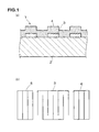
- Figs. 1(a) and 1(b) are a schematic partly cutaway front cross-sectional view of a surface acoustic wave device according to one embodiment of the present invention and a schematic plan view showing an electrode structure thereof, respectively.
- a surface acoustic wave device 1 has a piezoelectric substrate 2 composed of quartz having Euler angles of (0° ⁇ 5°, 0° to 140°, and 0° ⁇ 40°).
- An IDT electrode 3 is formed on the piezoelectric substrate 2.
- the IDT electrode 3 has a plurality of electrode fingers.
- a piezoelectric film 4 composed of c-axis oriented ZnO is formed on the piezoelectric substrate 2 so as to cover the IDT electrode 3.
- convex portions corresponding to the thickness of the IDT electrode are formed on the surface of the piezoelectric film 4.
- reflectors 5 and 6 are disposed at two sides of the IDT electrode 3 in a surface acoustic wave propagating direction.
- the surface acoustic wave device of this embodiment is a multi-mode resonator-type surface acoustic wave filter or a ladder filter resonator-type surface acoustic wave filter, and as the surface acoustic wave, a Rayleigh wave is used.
- the IDT electrode 3 described above is composed of a metal material primarily including at least one metal selected from the group consisting of Al, Au, Ta, W, Pt, Cu, Ni, and Mo.
- a normalized thickness of the IDT electrode normalized by the wavelength of the surface acoustic wave, and a normalized thickness of the piezoelectric film normalized by the wavelength of the surface acoustic wave are set within the ranges of each combination shown in the following Table 5.
- Table 5 Primary metal of IDT electrode Normalized thickness of IDT electrode Normalized ZnO thickness Al 0.02 ⁇ h/ ⁇ 0.2 0.03 ⁇ h/ ⁇ 0.3 Au 0.005 ⁇ h/ ⁇ 0.2 0.03 ⁇ h/ ⁇ 0.3 Ta 0.005 ⁇ h/ ⁇ 0.2 0.03 ⁇ h/ ⁇ 0.3 W 0.005 ⁇ h/ ⁇ 0.2 0.03 ⁇ h/ ⁇ 0.3 Pt 0.005 ⁇ h/ ⁇ 50.2 0.03 ⁇ h/ ⁇ 0.3 Cu 0.02 ⁇ h/ ⁇ 0.2 0.03 ⁇ h/ ⁇ 0.3 Ni 0.02 ⁇ h/ ⁇ 0.2 0.03 ⁇ h/ ⁇ 0.3 Mo 0.01 ⁇ h/ ⁇ 0.2 0.03 ⁇ h/ ⁇ 0.3
- the absolute value of the reflectivity coefficient of the surface acoustic wave per one electrode finger of the IDT electrode 3 can be increased to 0.025 or more, and a narrow bandpass resonator type surface acoustic wave filter having a narrow fractional bandwidth can be provided.
- Figs. 2 to 9 are views each showing the change in reflectivity coefficient per one electrode finger of an IDT which is obtained in such a way that as a piezoelectric substrate composed of quartz, a quartz substrate having Euler angles (0°, 117°, 0°) is used; Al, Au, Ta, W, Pt, Cu, Ni, or Mo is used as a metal material forming an IDT electrode; and a normalized thickness of an IDT electrode composed of one of the above metals normalized by the wavelength of a surface acoustic wave and a normalized thickness of a ZnO film normalized by the wavelength of the surface acoustic wave are changed.
- the absolute value of the reflectivity coefficient can be increased to 0.025 or more.
- Figs. 10 to 12 are views each showing the relationship of the reflectivity coefficient with the normalized thickness of the IDT electrode and the normalized thickness of the ZnO film which is obtained in such a way that an IDT electrode composed of Al, Au, or Cu is formed to have various thicknesses on a piezoelectric substrate of quartz having Euler angles (0°, 117°, 35°), and that the thickness of the ZnO thin film is variously changed.
- the combination in order to obtain a reflectivity coefficient of 0.05 or more, the combination may be set in the ranges of each combination shown in the following Table 6, and that, when the combination is set in the ranges of each combination shown in the following Table 7, the absolute value of the reflectivity coefficient can be increased to 0.1 or more.
- Table 6 Primary metal of IDT electrode Normalized thickness of IDT electrode Normalized ZnO thickness Al 0.06 ⁇ h/ ⁇ 0.2 0.03 ⁇ h/ ⁇ 0.3 Au 0.02 ⁇ h/ ⁇ 0.2 0.03 ⁇ h/ ⁇ 0.3 Ta 0.04 ⁇ h/ ⁇ 0.2 0.03 ⁇ h/ ⁇ 0.3 W 0.04 ⁇ h/ ⁇ 0.2 0.03 ⁇ h/ ⁇ 0.3 Pt 0.02 ⁇ h/ ⁇ 0.2 0.03 ⁇ h/ ⁇ 0.3 Cu 0.06 ⁇ h/ ⁇ 0.2 0.03 ⁇ h/ ⁇ 0.2 Ni 0.06 ⁇ h/ ⁇ 0.2 0.03 ⁇ h/ ⁇ 0.2 Mo 0.06 ⁇ h/ ⁇ 0.2 0.03 ⁇ h/ ⁇ 0.2
- Table 7 Primary metal of IDT electrode Normalized thickness of IDT electrode Normalized ZnO thickness Al 0.1 ⁇ h/ ⁇ 0.075 0.03 ⁇ h/ ⁇ 0.3 Au 0.06 ⁇ h/ ⁇ 0.075 0.03 ⁇ h/ ⁇ v0.3 Ta 0.06 ⁇ h/ ⁇ 0.075 0.03 ⁇ h/ ⁇ 0.3 W 0.06 ⁇ h/ ⁇ v0.075 0.03vh/ ⁇ 0.3 Pt 0.06 ⁇ h/ ⁇ 0.075 0.03 ⁇ h/ ⁇ 0.3 Cu 0.06 ⁇ h/ ⁇ 0.075 0.03 ⁇ h/ ⁇ 0.1 Ni 0.06 ⁇ h/ ⁇ 0.075 0.03 ⁇ h/ ⁇ 0.1 Mo 0.06 ⁇ h/ ⁇ 0.075 0.03 ⁇ h/ ⁇ 0.1
- the upper limit of the thickness of the IDT electrode be set to 0.08 ⁇ or less.
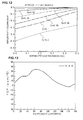
- Fig. 13 is a view showing the change in temperature coefficient of frequency TCF of a Rayleigh wave which is obtained when ⁇ of Euler angles (0°, ⁇ , 0°) of the piezoelectric substrate 2 composed of quartz in the surface acoustic wave device 1 is changed. As apparent from Fig. 13 , it is found that when ⁇ of Euler angles (0°, ⁇ , 0°) is in the range of 0° to 140°, the TCF is positive.
- the temperature coefficient of frequency TCF of a ZnO film is a negative value.
- the Euler angle ⁇ is set in the range of 0° to 140°, the temperature coefficient of frequency TCF of quartz is counteracted by that of the ZnO film, and that a surface acoustic wave device having a small temperature coefficient of frequency TCF can be provided.
- the Euler angles of the piezoelectric substrate 2 composed of quartz are preferably set to (0°, 0° to 140°, 0°).
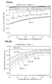
- Fig. 14 is a view showing the relationship between the temperature coefficient of frequency TCF and an Euler angle ⁇ .
- the solid line indicates the result obtained when quartz having Euler angles (0°, 119° 45', ⁇ ) is used, and the dotted line indicates the result obtained when quartz having Euler angles (0°, 132° 45', ⁇ ) is used.
- the TCF is positive.
- the temperature coefficient of frequency TCF of quartz can be counteracted by a negative temperature coefficient of frequency TCF of the ZnO film.
- the Euler angles of a piezoelectric substrate composed of quartz should be set in the range of (0°, 0° to 140°, 0° ⁇ 40°).
- the piezoelectric substrate 2 may be used which is composed of quartz having Euler angles (0° ⁇ 5°, 0° to 140°, 0° ⁇ 40°).
- the Euler angles are more preferably set in the range of (0° ⁇ 5°, 105° to 140°, 0° ⁇ 40°), and as a result, a surface acoustic wave device having more stable properties with the change in temperature can be provided.
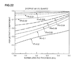
- Figs. 15 to 18 are views each showing the change in reflectivity coefficient of the structure in which an IDT composed of Al, Au, Cu, or Pt is formed to have various thicknesses on a piezoelectric substrate composed of quartz having Euler angles (0°, 132° 45', 0°), and in which the piezoelectric film 3 composed of ZnO is formed to have various thicknesses.
- the IDT electrode is formed of the above Al.
- the normalized thickness of the IDT electrode and the normalized thickness of the ZnO film are set within the ranges of each combination shown in Table 5, preferably within the ranges of each combination shown in Table 6, and more preferably within the ranges of each combination shown in Table 7, a surface acoustic wave device having a narrow bandwidth can be easily provided in which the absolute value of the temperature coefficient of frequency TCF is small, the temperature properties are stable, and the reflectivity coefficient of an electrode finger of the IDT electrode can be increased.
- the IDT electrode is formed of Al, Au, Ta, W, Pt, Cu, Ni, or Mo
- the IDT electrode is not always necessarily formed of the above pure metal. That is, the IDT electrode may be formed of a metal material primarily composed of at least one metal selected from the group consisting of Al, Au, Ta, W, Pt, Cu, Ni, and Mo.
- the metal material primarily composed of the above metal the metal described above or an alloy primarily containing the above metal may be used.
- the above metal material may be composed of a laminate metal film including a plurality of metal films laminated to each other, and in this case, the primary component of the whole laminate metal film may be one metal selected from the group consisting of Al, Au, Ta, W, Pt, Cu, Ni, and Mo or an alloy primarily containing the above metal.
- the IDT electrode may be a laminate metal film including a plurality of metal films formed of a plurality of metals selected from the group consisting of Al, Au, Ta, W, Pt, Cu, Ni, and Mo.
- the normalized thickness of the IDT electrode may be determined in consideration of the average density of the laminate metal film.
- the average density, the normalized thickness of the IDT electrode, and the normalized thickness of ZnO may be set within the ranges shown in the following Table 9.
- Table 9 Average density (kg/m 3 ) Normalized thickness of IDT electrode Normalized ZnO thickness 2,699 0.1 ⁇ h/ ⁇ 0.07S 0.03 ⁇ h/ ⁇ 0.3 8,845 0.06 ⁇ h/ ⁇ 0.075 0.03 ⁇ h/ ⁇ 0.1 8,930 0.06 ⁇ h/ ⁇ 0.075 0.03 ⁇ h/ ⁇ 0.1 10,219 0.06 ⁇ h/ ⁇ 0.075 0.03 ⁇ h/ ⁇ 0.1 16,678 0.06 ⁇ h/ ⁇ 0.075 0.03 ⁇ h/ ⁇ 0.3 19,265 0.06 ⁇ h/ ⁇ 0.075 0.03 ⁇ h/ ⁇ 0.3 19,300 0.06 ⁇ h/ ⁇ 0.075 0.03 ⁇ h/ ⁇ 0.3 21,400 0.06 ⁇ h/ ⁇ 0.075 0.03 ⁇ h/ ⁇ 0.3
- the normalized thickness of the IDT electrode and the normalized thickness range of the ZnO film are selected from one of those shown in Table 9, so that the reflectivity coefficient per one electrode finger can be made 0.1 or more.
- the average density of the IDT electrode composed of a laminate metal film is different from the average densities shown in the above Table 9, one combination at one of the average densities shown in Table 9 which is closest to the above density of the IDT electrode may be used instead.
- the thicknesses of five metal films composed of Ta, Pt, W, Au, and Mo are represented by a, b, c, d, and e, respectively, and the densities of the metal films are represented by ⁇ (Ta), ⁇ (Pt), ⁇ (W), ⁇ (Au), and ⁇ (Mo)
- the average density ⁇ ave is represented by ⁇ a ⁇ (Ta)+b ⁇ (Pt)+c ⁇ (W)+d ⁇ (Au)+e ⁇ (Mo) ⁇ /(a+b+c+d+e)
- the surface acoustic wave device of the present invention is not particularly limited as long as it is a resonator type and may be applied to various resonator type surface acoustic wave filters, such as a longitudinal coupling type, and one-port type surface acoustic wave resonators.
- cross-sectional shape of the convex portion of the piezoelectric film composed of ZnO is not limited to the shape shown in Fig. 1(a) and, for example, may be a trapezoid shape.
Landscapes
- Physics & Mathematics (AREA)
- Acoustics & Sound (AREA)
- Surface Acoustic Wave Elements And Circuit Networks Thereof (AREA)
Applications Claiming Priority (2)
| Application Number | Priority Date | Filing Date | Title |
|---|---|---|---|
| JP2006352091 | 2006-12-27 | ||
| PCT/JP2007/074018 WO2008081695A1 (ja) | 2006-12-27 | 2007-12-13 | 弾性表面波装置 |
Publications (2)
| Publication Number | Publication Date |
|---|---|
| EP2099129A1 true EP2099129A1 (de) | 2009-09-09 |
| EP2099129A4 EP2099129A4 (de) | 2014-03-26 |
Family
ID=39588379
Family Applications (1)
| Application Number | Title | Priority Date | Filing Date |
|---|---|---|---|
| EP07850538.5A Withdrawn EP2099129A4 (de) | 2006-12-27 | 2007-12-13 | Oberflächenwellenbauelement |
Country Status (5)
| Country | Link |
|---|---|
| US (1) | US7626314B2 (de) |
| EP (1) | EP2099129A4 (de) |
| JP (1) | JP4992911B2 (de) |
| CN (1) | CN101584115B (de) |
| WO (1) | WO2008081695A1 (de) |
Families Citing this family (12)
| Publication number | Priority date | Publication date | Assignee | Title |
|---|---|---|---|---|
| CN103262410B (zh) * | 2010-12-24 | 2016-08-10 | 株式会社村田制作所 | 弹性波装置及其制造方法 |
| JP6394710B2 (ja) * | 2015-01-07 | 2018-09-26 | 株式会社村田製作所 | 複合フィルタ装置 |
| JP6601503B2 (ja) | 2015-10-23 | 2019-11-06 | 株式会社村田製作所 | 弾性波装置、高周波フロントエンド回路及び通信装置 |
| CN108141198B (zh) * | 2015-10-23 | 2022-04-29 | 株式会社村田制作所 | 弹性波装置 |
| CN116599494A (zh) * | 2016-11-18 | 2023-08-15 | 株式会社村田制作所 | 声表面波滤波器以及多工器 |
| KR101953219B1 (ko) * | 2016-11-24 | 2019-02-28 | 가부시키가이샤 무라타 세이사쿠쇼 | 탄성파 장치, 고주파 프론트 엔드 회로 및 통신 장치 |
| DE112017005984B4 (de) * | 2016-11-25 | 2025-06-26 | Skyvvorks Solutions, Inc. (n.d.Ges.d.Staates Delaware) | Akustische Wellenvorrichtungen |
| CN107041751A (zh) * | 2017-04-01 | 2017-08-15 | 浙江大学 | 一种呼吸状态检测系统及无线无源的声表面波传感器 |
| JP6963423B2 (ja) * | 2017-06-14 | 2021-11-10 | 株式会社日本製鋼所 | 接合基板、弾性表面波素子および接合基板の製造方法 |
| JP2019062424A (ja) * | 2017-09-27 | 2019-04-18 | 株式会社村田製作所 | 弾性波装置、高周波フロントエンド回路及び通信装置 |
| FR3079667B1 (fr) * | 2018-03-28 | 2020-03-27 | Frec'n'sys | Dispositif d'onde acoustique de surface sur substrat composite |
| TWI689856B (zh) * | 2019-01-04 | 2020-04-01 | 友達光電股份有限公司 | 壓電感測器 |
Family Cites Families (24)
| Publication number | Priority date | Publication date | Assignee | Title |
|---|---|---|---|---|
| JPS61136312A (ja) * | 1984-12-06 | 1986-06-24 | Alps Electric Co Ltd | 弾性表面波素子 |
| JPH01292908A (ja) | 1988-05-20 | 1989-11-27 | Hitachi Ltd | 弾性表面波フィルタ |
| JPH0818388A (ja) * | 1993-09-16 | 1996-01-19 | Matsushita Electric Ind Co Ltd | 表面波フィルタ素子とその製造方法 |
| JP3205978B2 (ja) * | 1995-08-08 | 2001-09-04 | 住友電気工業株式会社 | 表面弾性波素子 |
| JP3196678B2 (ja) * | 1997-02-07 | 2001-08-06 | 株式会社村田製作所 | 表面波装置 |
| US6377138B1 (en) | 1997-07-28 | 2002-04-23 | Kabushiki Kaisha Toshiba | Surface acoustic wave device with a layered conductive film and method of producing the same |
| JPH11136083A (ja) * | 1997-08-27 | 1999-05-21 | Murata Mfg Co Ltd | 表面波装置 |
| JP3301399B2 (ja) | 1998-02-16 | 2002-07-15 | 株式会社村田製作所 | 弾性表面波装置 |
| JP3568025B2 (ja) | 1999-05-14 | 2004-09-22 | 株式会社村田製作所 | 表面波装置及び通信機装置 |
| JP3341759B2 (ja) * | 1999-10-15 | 2002-11-05 | 住友電気工業株式会社 | 表面弾性波素子 |
| JP2002280856A (ja) * | 2001-03-21 | 2002-09-27 | Seiko Epson Corp | 弾性表面波素子の製造方法 |
| US6717327B2 (en) * | 2001-04-23 | 2004-04-06 | Murata Manufacturing Co., Ltd. | Surface acoustic wave device |
| JP2003037467A (ja) * | 2001-07-24 | 2003-02-07 | Murata Mfg Co Ltd | 弾性表面波装置 |
| JP3841053B2 (ja) * | 2002-07-24 | 2006-11-01 | 株式会社村田製作所 | 弾性表面波装置及びその製造方法 |
| JP4145678B2 (ja) * | 2003-02-13 | 2008-09-03 | セイコーエプソン株式会社 | 縦2重モード型sawフィルタ |
| JP4244656B2 (ja) * | 2003-02-26 | 2009-03-25 | 株式会社村田製作所 | 弾性表面波装置 |
| JP4158650B2 (ja) * | 2003-08-20 | 2008-10-01 | セイコーエプソン株式会社 | 弾性表面波デバイス及びその製造方法 |
| CN100495910C (zh) * | 2003-10-29 | 2009-06-03 | 株式会社村田制作所 | 弹性表面波装置 |
| JP2005142629A (ja) | 2003-11-04 | 2005-06-02 | Seiko Epson Corp | 弾性表面波素子およびその製造方法 |
| JP4497159B2 (ja) * | 2004-04-08 | 2010-07-07 | 株式会社村田製作所 | 弾性境界波フィルタ |
| JP4483865B2 (ja) * | 2004-07-26 | 2010-06-16 | 株式会社村田製作所 | 弾性表面波装置 |
| JP4548088B2 (ja) | 2004-10-20 | 2010-09-22 | セイコーエプソン株式会社 | 弾性表面波装置 |
| EP1675260A3 (de) * | 2004-12-03 | 2007-08-15 | Epson Toyocom Corporation | Akustische Oberflächenwellenvorrichtung |
| JPWO2006137464A1 (ja) * | 2005-06-21 | 2009-01-22 | エプソントヨコム株式会社 | 弾性表面波デバイス、モジュール、及び発振器 |
-
2007
- 2007-12-13 EP EP07850538.5A patent/EP2099129A4/de not_active Withdrawn
- 2007-12-13 JP JP2008552078A patent/JP4992911B2/ja not_active Expired - Fee Related
- 2007-12-13 WO PCT/JP2007/074018 patent/WO2008081695A1/ja not_active Ceased
- 2007-12-13 CN CN2007800479298A patent/CN101584115B/zh not_active Expired - Fee Related
-
2009
- 2009-06-03 US US12/477,282 patent/US7626314B2/en active Active
Also Published As
| Publication number | Publication date |
|---|---|
| US20090237181A1 (en) | 2009-09-24 |
| JPWO2008081695A1 (ja) | 2010-04-30 |
| US7626314B2 (en) | 2009-12-01 |
| JP4992911B2 (ja) | 2012-08-08 |
| WO2008081695A1 (ja) | 2008-07-10 |
| CN101584115A (zh) | 2009-11-18 |
| CN101584115B (zh) | 2012-09-05 |
| EP2099129A4 (de) | 2014-03-26 |
Similar Documents
| Publication | Publication Date | Title |
|---|---|---|
| EP2099129A1 (de) | Oberflächenwellenbauelement | |
| US8183737B2 (en) | Surface acoustic wave device including electrode fingers partially disposed in grooves in a piezoelectric substrate | |
| EP2744107B1 (de) | Elastische wellenvorrichtung | |
| EP1391988B1 (de) | Oberflächenwellen-Bauelement und Verfahren zu seiner Herstellung | |
| US9419584B2 (en) | Antenna sharing device | |
| US7569972B2 (en) | Surface acoustic wave device | |
| US7315107B2 (en) | Surface acoustic wave device | |
| JP5338914B2 (ja) | 弾性波素子と、これを用いたデュプレクサおよび電子機器 | |
| US7876021B2 (en) | Surface acoustic wave device including an IDT defined by a metal filled in grooves in a piezoelectric substrate | |
| EP2068442B1 (de) | Grenzschallwellenvorrichtung | |
| US20230208387A1 (en) | Elastic wave device | |
| EP1990915A1 (de) | Oberflächenwellenanordnung und verfahren zu ihrer herstellung | |
| JP2001077662A (ja) | 表面波装置及び通信機装置 | |
| US7212080B2 (en) | Surface acoustic wave device having two piezoelectric substrates with different cut angles | |
| Kadota et al. | Ultrawide-band resonators using shear horizontal-type plate wave and their application | |
| EP1883158A1 (de) | Elastische grenzwellenvorrichtung | |
| US6914498B2 (en) | Surface acoustic wave device on LiTaO3 substrate using primarily silver electrodes covered with SiO2 film | |
| JP2003258602A (ja) | 弾性表面波装置 | |
| US7956512B2 (en) | Surface acoustic wave device including an IDT formed by a metal filled in grooves on a piezoelectric substrate | |
| JP2009194895A (ja) | 弾性表面波装置 | |
| JP4811517B2 (ja) | 弾性表面波装置 | |
| JP2012227626A (ja) | 弾性表面波素子 | |
| JP4992968B2 (ja) | 弾性表面波装置 | |
| JP2010283807A (ja) | 弾性表面波装置 | |
| JP3196474B2 (ja) | 表面波装置 |
Legal Events
| Date | Code | Title | Description |
|---|---|---|---|
| PUAI | Public reference made under article 153(3) epc to a published international application that has entered the european phase |
Free format text: ORIGINAL CODE: 0009012 |
|
| 17P | Request for examination filed |
Effective date: 20090611 |
|
| AK | Designated contracting states |
Kind code of ref document: A1 Designated state(s): AT BE BG CH CY CZ DE DK EE ES FI FR GB GR HU IE IS IT LI LT LU LV MC MT NL PL PT RO SE SI SK TR |
|
| DAX | Request for extension of the european patent (deleted) | ||
| A4 | Supplementary search report drawn up and despatched |
Effective date: 20140226 |
|
| RIC1 | Information provided on ipc code assigned before grant |
Ipc: H03H 9/145 20060101ALI20140220BHEP Ipc: H03H 9/02 20060101AFI20140220BHEP |
|
| 17Q | First examination report despatched |
Effective date: 20160421 |
|
| GRAP | Despatch of communication of intention to grant a patent |
Free format text: ORIGINAL CODE: EPIDOSNIGR1 |
|
| INTG | Intention to grant announced |
Effective date: 20171102 |
|
| RAP1 | Party data changed (applicant data changed or rights of an application transferred) |
Owner name: MURATA MANUFACTURING CO., LTD. |
|
| RIN1 | Information on inventor provided before grant (corrected) |
Inventor name: KADOTA, MICHIO |
|
| STAA | Information on the status of an ep patent application or granted ep patent |
Free format text: STATUS: THE APPLICATION IS DEEMED TO BE WITHDRAWN |
|
| 18D | Application deemed to be withdrawn |
Effective date: 20180313 |