EP2100185B1 - Unité de rétroéclairage et afficheur équipé de cette unité - Google Patents
Unité de rétroéclairage et afficheur équipé de cette unité Download PDFInfo
- Publication number
- EP2100185B1 EP2100185B1 EP07851642A EP07851642A EP2100185B1 EP 2100185 B1 EP2100185 B1 EP 2100185B1 EP 07851642 A EP07851642 A EP 07851642A EP 07851642 A EP07851642 A EP 07851642A EP 2100185 B1 EP2100185 B1 EP 2100185B1
- Authority
- EP
- European Patent Office
- Prior art keywords
- reflective sheet
- led
- backlight unit
- fixing part
- led module
- Prior art date
- Legal status (The legal status is an assumption and is not a legal conclusion. Google has not performed a legal analysis and makes no representation as to the accuracy of the status listed.)
- Active
Links
Images
Classifications
-
- G—PHYSICS
- G02—OPTICS
- G02F—OPTICAL DEVICES OR ARRANGEMENTS FOR THE CONTROL OF LIGHT BY MODIFICATION OF THE OPTICAL PROPERTIES OF THE MEDIA OF THE ELEMENTS INVOLVED THEREIN; NON-LINEAR OPTICS; FREQUENCY-CHANGING OF LIGHT; OPTICAL LOGIC ELEMENTS; OPTICAL ANALOGUE/DIGITAL CONVERTERS
- G02F1/00—Devices or arrangements for the control of the intensity, colour, phase, polarisation or direction of light arriving from an independent light source, e.g. switching, gating or modulating; Non-linear optics
- G02F1/01—Devices or arrangements for the control of the intensity, colour, phase, polarisation or direction of light arriving from an independent light source, e.g. switching, gating or modulating; Non-linear optics for the control of the intensity, phase, polarisation or colour
- G02F1/13—Devices or arrangements for the control of the intensity, colour, phase, polarisation or direction of light arriving from an independent light source, e.g. switching, gating or modulating; Non-linear optics for the control of the intensity, phase, polarisation or colour based on liquid crystals, e.g. single liquid crystal display cells
- G02F1/133—Constructional arrangements; Operation of liquid crystal cells; Circuit arrangements
- G02F1/1333—Constructional arrangements; Manufacturing methods
- G02F1/1335—Structural association of cells with optical devices, e.g. polarisers or reflectors
-
- G—PHYSICS
- G02—OPTICS
- G02F—OPTICAL DEVICES OR ARRANGEMENTS FOR THE CONTROL OF LIGHT BY MODIFICATION OF THE OPTICAL PROPERTIES OF THE MEDIA OF THE ELEMENTS INVOLVED THEREIN; NON-LINEAR OPTICS; FREQUENCY-CHANGING OF LIGHT; OPTICAL LOGIC ELEMENTS; OPTICAL ANALOGUE/DIGITAL CONVERTERS
- G02F1/00—Devices or arrangements for the control of the intensity, colour, phase, polarisation or direction of light arriving from an independent light source, e.g. switching, gating or modulating; Non-linear optics
- G02F1/01—Devices or arrangements for the control of the intensity, colour, phase, polarisation or direction of light arriving from an independent light source, e.g. switching, gating or modulating; Non-linear optics for the control of the intensity, phase, polarisation or colour
- G02F1/13—Devices or arrangements for the control of the intensity, colour, phase, polarisation or direction of light arriving from an independent light source, e.g. switching, gating or modulating; Non-linear optics for the control of the intensity, phase, polarisation or colour based on liquid crystals, e.g. single liquid crystal display cells
- G02F1/133—Constructional arrangements; Operation of liquid crystal cells; Circuit arrangements
- G02F1/1333—Constructional arrangements; Manufacturing methods
- G02F1/1335—Structural association of cells with optical devices, e.g. polarisers or reflectors
- G02F1/1336—Illuminating devices
- G02F1/133602—Direct backlight
- G02F1/133603—Direct backlight with LEDs
-
- G—PHYSICS
- G02—OPTICS
- G02F—OPTICAL DEVICES OR ARRANGEMENTS FOR THE CONTROL OF LIGHT BY MODIFICATION OF THE OPTICAL PROPERTIES OF THE MEDIA OF THE ELEMENTS INVOLVED THEREIN; NON-LINEAR OPTICS; FREQUENCY-CHANGING OF LIGHT; OPTICAL LOGIC ELEMENTS; OPTICAL ANALOGUE/DIGITAL CONVERTERS
- G02F1/00—Devices or arrangements for the control of the intensity, colour, phase, polarisation or direction of light arriving from an independent light source, e.g. switching, gating or modulating; Non-linear optics
- G02F1/01—Devices or arrangements for the control of the intensity, colour, phase, polarisation or direction of light arriving from an independent light source, e.g. switching, gating or modulating; Non-linear optics for the control of the intensity, phase, polarisation or colour
- G02F1/13—Devices or arrangements for the control of the intensity, colour, phase, polarisation or direction of light arriving from an independent light source, e.g. switching, gating or modulating; Non-linear optics for the control of the intensity, phase, polarisation or colour based on liquid crystals, e.g. single liquid crystal display cells
- G02F1/133—Constructional arrangements; Operation of liquid crystal cells; Circuit arrangements
- G02F1/1333—Constructional arrangements; Manufacturing methods
- G02F1/1335—Structural association of cells with optical devices, e.g. polarisers or reflectors
- G02F1/1336—Illuminating devices
- G02F1/133602—Direct backlight
- G02F1/133605—Direct backlight including specially adapted reflectors
-
- G—PHYSICS
- G02—OPTICS
- G02F—OPTICAL DEVICES OR ARRANGEMENTS FOR THE CONTROL OF LIGHT BY MODIFICATION OF THE OPTICAL PROPERTIES OF THE MEDIA OF THE ELEMENTS INVOLVED THEREIN; NON-LINEAR OPTICS; FREQUENCY-CHANGING OF LIGHT; OPTICAL LOGIC ELEMENTS; OPTICAL ANALOGUE/DIGITAL CONVERTERS
- G02F1/00—Devices or arrangements for the control of the intensity, colour, phase, polarisation or direction of light arriving from an independent light source, e.g. switching, gating or modulating; Non-linear optics
- G02F1/01—Devices or arrangements for the control of the intensity, colour, phase, polarisation or direction of light arriving from an independent light source, e.g. switching, gating or modulating; Non-linear optics for the control of the intensity, phase, polarisation or colour
- G02F1/13—Devices or arrangements for the control of the intensity, colour, phase, polarisation or direction of light arriving from an independent light source, e.g. switching, gating or modulating; Non-linear optics for the control of the intensity, phase, polarisation or colour based on liquid crystals, e.g. single liquid crystal display cells
- G02F1/133—Constructional arrangements; Operation of liquid crystal cells; Circuit arrangements
- G02F1/1333—Constructional arrangements; Manufacturing methods
- G02F1/1335—Structural association of cells with optical devices, e.g. polarisers or reflectors
- G02F1/1336—Illuminating devices
- G02F1/133602—Direct backlight
- G02F1/133608—Direct backlight including particular frames or supporting means
-
- G—PHYSICS
- G02—OPTICS
- G02F—OPTICAL DEVICES OR ARRANGEMENTS FOR THE CONTROL OF LIGHT BY MODIFICATION OF THE OPTICAL PROPERTIES OF THE MEDIA OF THE ELEMENTS INVOLVED THEREIN; NON-LINEAR OPTICS; FREQUENCY-CHANGING OF LIGHT; OPTICAL LOGIC ELEMENTS; OPTICAL ANALOGUE/DIGITAL CONVERTERS
- G02F1/00—Devices or arrangements for the control of the intensity, colour, phase, polarisation or direction of light arriving from an independent light source, e.g. switching, gating or modulating; Non-linear optics
- G02F1/01—Devices or arrangements for the control of the intensity, colour, phase, polarisation or direction of light arriving from an independent light source, e.g. switching, gating or modulating; Non-linear optics for the control of the intensity, phase, polarisation or colour
- G02F1/13—Devices or arrangements for the control of the intensity, colour, phase, polarisation or direction of light arriving from an independent light source, e.g. switching, gating or modulating; Non-linear optics for the control of the intensity, phase, polarisation or colour based on liquid crystals, e.g. single liquid crystal display cells
- G02F1/133—Constructional arrangements; Operation of liquid crystal cells; Circuit arrangements
- G02F1/1333—Constructional arrangements; Manufacturing methods
- G02F1/1335—Structural association of cells with optical devices, e.g. polarisers or reflectors
- G02F1/1336—Illuminating devices
- G02F1/133602—Direct backlight
- G02F1/133611—Direct backlight including means for improving the brightness uniformity
Definitions
- the embodiment relates to a backlight unit for a display device.
- FIG. 1 is a view schematically showing a conventional backlight unit.
- the conventional backlight unit comprises an LED module 10, a case 20, a fixing part 30 and a reflective sheet 40.
- the LED module 10 comprises a printed circuit board 11, an LED 13 formed on the printed circuit board 11, and a mold part 15 formed on the LED 13.
- the reflective sheet 40 reflects light, which is emitted from the LED 13, in the upward direction.
- the reflective sheet 40 is formed with an opening for exposing the LED 13.
- the reflective sheet 40 has reflectivity of 98% or more.
- the fixing part 30 fixes the reflective sheet 40 and the LED module 10 to the case 20.
- the case 20 may be a cover bottom.
- An upper portion of the fixing part 30 is exposed on the reflective sheet 40.
- the fixing part 30 comprises a screw.
- the fixing part 30 has reflectivity of about 60 to 70%.
- FIG. 2 is a view showing a problem of the conventional backlight unit.
- An optical sheet 70 such as a diffusion sheet, can be aligned on the backlight unit. Since the fixing part 30 has relatively low reflectivity, brightness of a region where the fixing part 30 is positioned may be lowered relative to other regions. Thus, a dark line may occur in the region where the fixing part 30 is positioned, causing non-uniform brightness distribution.
- document US 2006/104080 A1 on which the preamble of claim 1 is based discloses a backlight unit, and more particularly, a backlight unit employing a light emitting diode (LED) module as a light source.
- LED light emitting diode
- Document JP 2006 058487 A discloses a heat radiating device in which a heat-radiating plate, a back plate, and a heat sink, constituting a heat conducting route to radiate heat, while retaining a state of tight adherence.
- Document EP 1 925 971 A2 which represents prior art only in the sense of Article 54(3) EPC, discloses a light source apparatus using a LED, a back-light apparatus equipped with the light source apparatus, a liquid crystal display apparatus equipped with the back-light apparatus, and a manufacturing method of the back-light apparatus.
- the embodiment provides a backlight unit as defined in claim 1, which is capable of improving brightness uniformity.
- the backlight unit according to the embodiment can improve brightness uniformity.
- FIG. 3 is a view schematically showing a backlight unit As shown in FIG. 3 , the backlight unit comprises an LED module 110, a case 120, a fixing part 130, a reflective sheet 140, and a guide pin 150.
- the backlight unit comprises an LED module 110, a case 120, a fixing part 130, a reflective sheet 140, and a guide pin 150.
- the LED module 110 comprises a printed circuit board 111, an LED 113 disposed on the printed circuit board 111, and a mold part 115 formed on the LED 113.
- the LED 113 can be mounted on the printed circuit board 111.
- the LED module 110 may be formed with at least three LED, and disposed with at least one column and two rows.
- the case 120 supports the LED module 110.
- the reflective sheet 140 is formed on the LED module 110 and the fixing part 130.
- the case 120 may be a cover bottom.
- the guide pin 150 fixes the reflective sheet 140 to the case 120.
- the guide pin 150 can support an optical sheet, such as a diffusion sheet mounted on the guide pin 150.
- the guide pin 150 has reflectivity substantially identical or similar to that of the reflective sheet 140.
- the guide pin 150 can be inserted into the case 120 or can extend by passing through the case 120.
- the reflective sheet 140 reflects light emitted from the LED 113 in the upward direction.
- the reflective sheet 140 is formed with an opening for exposing the LED 113.
- the reflective sheet 140 represents reflectivity of 98% or more.
- the fixing part 130 fixes the LED module 110 to the case 120.
- the fixing part 130 comprises a screw and represents reflectivity of 60 to 70%.
- the fixing part 130 can be inserted into the case 120 or can extend by passing through the case 120.
- the fixing part 130 is positioned below the reflective sheet 140.
- the light reflected from the reflective sheet 140 in the upward direction may have uniform brightness.
- a stepped portion can be formed in a predetermined region of the reflective sheet 140 in correspondence with the fixing part 130 such that a protrusion of the fixing part 130 can be inserted into the stepped portion of the reflective sheet 140.
- the reflective sheet 140 may have a flat upper surface even in the region corresponding to the fixing part 130.
- a recess can be formed in a predetermined region of the reflective sheet 140 in correspondence with the fixing part 130 such that a protrusion of the fixing part 130 can be inserted into the recess portion of the reflective sheet 140.
- the reflective sheet 140 may have a flat upper surface even in the region corresponding to the fixing part 130.
- the backlight unit having the above structure is applicable for various display devices requiring the light sources.
- the backlight unit can be used for a liquid crystal display device comprising a liquid crystal panel.
- the liquid crystal display device displays an image on a display unit comprising the liquid crystal panel by using the light provided from the backlight unit. Since the liquid crystal display device comprises the backlight unit providing the light having uniform brightness, the liquid crystal display device can display a high-quality image.
- FIG. 4 is a view schematically showing a backlight unit according an embodiment
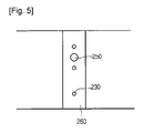
- FIG. 5 is a view showing a stack structure of first and second reflective sheets shown in FIG. 4 .
- the backlight unit of the embodiment comprises an LED module 210, a case 220, a fixing part 230, a first reflective sheet 240, a guide pin 250, and a second reflective sheet 260.
- the LED module 210 comprises a printed circuit board 211, an LED 213 disposed on the printed circuit board 211, and a mold part 215 formed on the LED 213.
- the LED 213 can be mounted on the printed circuit board 211.
- the LED module 210 may be formed with at least three LED, and disposed with at least one column and two rows.
- the case 220 supports the LED module 210.
- the case 220 may be a cover bottom.
- the first reflective sheet 240 is formed on the LED module 210 and has an opening for exposing the LED 213.
- the fixing part 230 fixes the first reflective sheet 240 and the LED module 210 to the case 220.
- An upper portion of the fixing part 230 is exposed out of the upper surface of the first reflective sheet 240.
- the fixing part 230 comprises a screw and represents reflectivity of 60 to 70%. If the fixing part 230 is prepared as a screw, the upper portion of the fixing part 230 can be prevented from being exposed out of the upper surface of the first reflective sheet 240 by increasing fastening force of the fixing part 230.
- the fixing part 230 can be inserted into the case 220 or can extend by passing through the case 220.
- the exposed fixing part 230 may cause non-uniform brightness.
- the second reflective sheet 260 is formed on the fixing part 230.
- the second reflective sheet 260 may be formed with the same columns or rows of the fixing part 230.
- the guide pin 250 fixes the second reflective sheet 260 to the case 220.
- the guide pin 250 can support an optical sheet, such as a diffusion sheet mounted on the guide pin 250.
- the guide pin 250 has reflectivity substantially identical or similar to that of the first and second reflective sheet 240 and 260.
- the first and second reflective sheets 240 and 260 reflect light emitted from the LED 213 in the upward direction.
- the first reflective sheet 240 is formed with an opening for exposing the LED 213.
- the first and second reflective sheets 240 and 260 represent reflectivity of 98% or more.
- a stepped portion can be formed in a predetermined region of the second reflective sheet 260 in correspondence with the fixing part 230 such that a protrusion of the fixing part 230 can be inserted into the stepped portion of the second reflective sheet 260.
- the second reflective sheet 260 may have a flat upper surface even in the region corresponding to the fixing part 230.
- a recess can be formed in a predetermined region of the second reflective sheet 260 in correspondence with the fixing part 230 such that a protrusion of the fixing part 230 can be inserted into the recess portion of the second reflective sheet 260.
- the second reflective sheet 260 may have a flat upper surface even in the region corresponding to the fixing part 230.
- the second reflective sheet 260 may have a thickness smaller than that of the first reflective sheet 240.
- the brightness distribution by the second reflective sheet 260 can be improved more than the second reflective sheet 260 is not exited.
- the backlight unit having the above structure is applicable for various display devices requiring the light sources.
- the backlight unit can be used for a liquid crystal display device comprising a liquid crystal panel.
- the liquid crystal display device displays an image on a display unit comprising the liquid crystal panel by using the light provided from the backlight unit. Since the liquid crystal display device comprises the backlight unit providing the light having uniform brightness, the liquid crystal display device can display a high-quality image.
- any reference in this specification to "one embodiment”, “an embodiment”, “example embodiment”, etc. means that a particular feature, structure, or characteristic described in connection with the embodiment is included in at least one embodiment of the invention.
- the appearances of such phrases in various places in the specification are not necessarily all referring to the same embodiment.
- the backlight unit according to the embodiment can improve brightness uniformity.
Landscapes
- Physics & Mathematics (AREA)
- Nonlinear Science (AREA)
- Mathematical Physics (AREA)
- Chemical & Material Sciences (AREA)
- Crystallography & Structural Chemistry (AREA)
- General Physics & Mathematics (AREA)
- Optics & Photonics (AREA)
- Planar Illumination Modules (AREA)
- Devices For Indicating Variable Information By Combining Individual Elements (AREA)
- Fastening Of Light Sources Or Lamp Holders (AREA)
Claims (5)
- Unité rétroéclairée comprenant :un module de DEL (210) comprenant une DEL (213) ;un boîtier (220) supportant le module de DEL ;une première feuille réfléchissante (240) comprenant une ouverture pour exposer la DEL sur le module de DEL ;une partie de fixation (230) fixant le module de DEL et la première feuille réfléchissante sur le boîtier ;une deuxième feuille réfléchissante (260) sur la partie de fixation ; etune tige de guidage (250) fixant la deuxième feuille réfléchissante sur le boîtier ;caractérisée en ce que la deuxième feuille réfléchissante comprend une portion étagée ou un évidement de sorte qu'une saillie de la partie de fixation soit reçue par la partie étagée ou l'évidement.
- Unité rétroéclairée selon la revendication 1, dans laquelle le module de DEL (210) comprend une carte de circuit imprimé (211), la DEL (213) sur la carte de circuit imprimé, et une partie moulée (215) sur la DEL.
- Unité rétroéclairée selon la revendication 1, dans laquelle les première et deuxième feuilles réfléchissantes ont une réflectivité sensiblement égale à celle de la tige de guidage (250).
- Unité rétroéclairée selon la revendication 1, dans laquelle la deuxième feuille réfléchissante a une épaisseur inférieure à celle de la première feuille réfléchissante.
- Unité rétroéclairée selon la revendication 1, dans laquelle le module de DEL comprend au moins trois DEL disposées sur au moins une colonne et deux rangées.
Applications Claiming Priority (2)
| Application Number | Priority Date | Filing Date | Title |
|---|---|---|---|
| KR1020060138963A KR100851164B1 (ko) | 2006-12-29 | 2006-12-29 | 백라이트 유닛 및 이를 구비하는 표시장치 |
| PCT/KR2007/006676 WO2008082105A1 (fr) | 2006-12-29 | 2007-12-20 | Unité de rétroéclairage et afficheur équipé de cette unité |
Publications (3)
| Publication Number | Publication Date |
|---|---|
| EP2100185A1 EP2100185A1 (fr) | 2009-09-16 |
| EP2100185A4 EP2100185A4 (fr) | 2010-09-15 |
| EP2100185B1 true EP2100185B1 (fr) | 2012-01-11 |
Family
ID=39588733
Family Applications (1)
| Application Number | Title | Priority Date | Filing Date |
|---|---|---|---|
| EP07851642A Active EP2100185B1 (fr) | 2006-12-29 | 2007-12-20 | Unité de rétroéclairage et afficheur équipé de cette unité |
Country Status (7)
| Country | Link |
|---|---|
| US (1) | US8045091B2 (fr) |
| EP (1) | EP2100185B1 (fr) |
| JP (1) | JP2010515218A (fr) |
| KR (1) | KR100851164B1 (fr) |
| CN (1) | CN101573654A (fr) |
| AT (1) | ATE541233T1 (fr) |
| WO (1) | WO2008082105A1 (fr) |
Families Citing this family (13)
| Publication number | Priority date | Publication date | Assignee | Title |
|---|---|---|---|---|
| KR100793514B1 (ko) * | 2006-12-29 | 2008-01-14 | 엘지이노텍 주식회사 | 백라이트 유닛 및 이를 구비하는 표시장치 |
| TWI407054B (zh) | 2008-09-17 | 2013-09-01 | Advanced Optoelectronic Tech | 發光二極體之光源組及其反射片組 |
| KR101006771B1 (ko) * | 2008-09-17 | 2011-01-10 | 주식회사 루멘스 | 백라이트 어셈블리 |
| CN101726881B (zh) * | 2008-10-10 | 2011-12-07 | 群康科技(深圳)有限公司 | 液晶显示装置 |
| JP5351723B2 (ja) | 2009-05-22 | 2013-11-27 | シャープ株式会社 | 光源装置及び表示装置 |
| JP4621799B1 (ja) | 2009-05-22 | 2011-01-26 | シャープ株式会社 | 光反射シート、光源装置及び表示装置 |
| JP4519944B1 (ja) | 2009-05-22 | 2010-08-04 | シャープ株式会社 | 光源装置及び表示装置 |
| KR101628228B1 (ko) * | 2009-09-10 | 2016-06-09 | 삼성디스플레이 주식회사 | 백라이트 어셈블리 및 이를 포함하는 표시 장치 |
| WO2012036060A1 (fr) * | 2010-09-15 | 2012-03-22 | シャープ株式会社 | Dispositif d'éclairage et procédé d'affichage |
| US20120092887A1 (en) * | 2010-10-15 | 2012-04-19 | Shenzhen China Star Optoelectronics Technology Co., Ltd. | Backlight module and display apparatus |
| CN102563447A (zh) * | 2010-12-30 | 2012-07-11 | 苏州世鼎电子有限公司 | 具有高工艺良率的led背光模块及其制造方法 |
| KR102137135B1 (ko) | 2014-01-29 | 2020-07-27 | 삼성디스플레이 주식회사 | 백라이트 어셈블리 및 이를 포함하는 표시 장치 |
| EP4513262A1 (fr) | 2023-08-22 | 2025-02-26 | Arçelik Anonim Sirketi | Dispositif d'affichage d'image de rétroéclairage |
Family Cites Families (14)
| Publication number | Priority date | Publication date | Assignee | Title |
|---|---|---|---|---|
| US6473554B1 (en) | 1996-12-12 | 2002-10-29 | Teledyne Lighting And Display Products, Inc. | Lighting apparatus having low profile |
| CA2402037C (fr) * | 1999-07-21 | 2010-03-09 | Teledyne Lighting And Display Products, Inc. | Appareil d'eclairage |
| JP2005159082A (ja) * | 2003-11-27 | 2005-06-16 | Kyocera Corp | 発光素子収納用パッケージおよび発光装置ならびに発光素子収納用パッケージの製造方法。 |
| KR20050122987A (ko) * | 2004-06-26 | 2005-12-29 | 엘지.필립스 엘시디 주식회사 | 직하형 백라이트 유닛 및 이를 구비한 액정표시장치 |
| JP4543813B2 (ja) | 2004-08-04 | 2010-09-15 | ソニー株式会社 | バックライト装置及びこのバックライト装置を備えた液晶表示装置 |
| JP4706206B2 (ja) * | 2004-08-18 | 2011-06-22 | ソニー株式会社 | 放熱装置及び表示装置 |
| KR101073043B1 (ko) | 2004-11-16 | 2011-10-12 | 삼성전자주식회사 | 표시 장치 |
| KR100609057B1 (ko) | 2004-11-17 | 2006-08-09 | 삼성전자주식회사 | 백라이트유닛 |
| KR101122216B1 (ko) | 2004-11-29 | 2012-03-19 | 삼성전자주식회사 | 백라이트 어셈블리 및 표시장치 |
| JP2006339004A (ja) * | 2005-06-01 | 2006-12-14 | Sony Corp | バックライト装置及び液晶表示装置 |
| JP2006349796A (ja) * | 2005-06-14 | 2006-12-28 | Sony Corp | 面状光源装置、及び、液晶表示装置組立体 |
| JP2008003254A (ja) * | 2006-06-21 | 2008-01-10 | Idemitsu Kosan Co Ltd | 光線反射用多層シート、これを用いた反射器、照明装置及び液晶表示装置 |
| JP5050498B2 (ja) | 2006-11-21 | 2012-10-17 | ソニー株式会社 | 光源装置、バックライト装置、液晶表示装置及びバックライト装置の製造方法 |
| KR101277854B1 (ko) * | 2009-02-18 | 2013-06-21 | 엘지디스플레이 주식회사 | 백라이트 유닛 및 이를 구비한 액정표시장치 |
-
2006
- 2006-12-29 KR KR1020060138963A patent/KR100851164B1/ko not_active Expired - Fee Related
-
2007
- 2007-12-20 WO PCT/KR2007/006676 patent/WO2008082105A1/fr not_active Ceased
- 2007-12-20 JP JP2009543923A patent/JP2010515218A/ja active Pending
- 2007-12-20 AT AT07851642T patent/ATE541233T1/de active
- 2007-12-20 CN CNA2007800487843A patent/CN101573654A/zh active Pending
- 2007-12-20 US US12/514,599 patent/US8045091B2/en active Active - Reinstated
- 2007-12-20 EP EP07851642A patent/EP2100185B1/fr active Active
Also Published As
| Publication number | Publication date |
|---|---|
| WO2008082105A1 (fr) | 2008-07-10 |
| EP2100185A1 (fr) | 2009-09-16 |
| ATE541233T1 (de) | 2012-01-15 |
| KR100851164B1 (ko) | 2008-08-08 |
| JP2010515218A (ja) | 2010-05-06 |
| EP2100185A4 (fr) | 2010-09-15 |
| KR20080062827A (ko) | 2008-07-03 |
| CN101573654A (zh) | 2009-11-04 |
| US20100026928A1 (en) | 2010-02-04 |
| US8045091B2 (en) | 2011-10-25 |
Similar Documents
| Publication | Publication Date | Title |
|---|---|---|
| US8045091B2 (en) | Backlight unit and dislay device having the same | |
| EP1998197B1 (fr) | Plaque de guide lumineux, ensemble de rétroéclairage l'incluant, et dispositif d'affichage à cristaux liquides l'incluant | |
| US8698972B2 (en) | Liquid crystal display device | |
| US8801209B2 (en) | Backlight assembly and display device having lower profile and/or reduced weight | |
| US20090174996A1 (en) | Display device | |
| US8746952B2 (en) | Illumination apparatus, display apparatus, and electronic device | |
| US9170365B2 (en) | Illumination apparatus, display apparatus, and electronic device | |
| KR20100048472A (ko) | 액정표시장치 및 이의 조립방법 | |
| KR20120019140A (ko) | 액정표시장치 | |
| JP2010210891A (ja) | 液晶表示装置 | |
| US20190285945A1 (en) | Lighting device and display device including the same | |
| US20140002765A1 (en) | Liquid crystal display module and liquid crystal display device having the same | |
| KR101308873B1 (ko) | 액정표시장치 | |
| EP3279720B1 (fr) | Unité de rétroéclairage dotée d'un élément de support d'unité de source de lumière, procédé de fabrication de l'élément de support et afficheur comprenant l'unité de rétroéclairage | |
| US10914985B2 (en) | Image display apparatus and support pin | |
| US10914984B2 (en) | Image display apparatus and support pin | |
| US11841527B2 (en) | Backlight module and display device | |
| US20120212974A1 (en) | Display module and display apparatus | |
| US9453959B2 (en) | Backlight unit and display apparatus | |
| KR20080013311A (ko) | 액정 표시 장치 | |
| KR20200099225A (ko) | 표시 장치 | |
| KR101222960B1 (ko) | 액정표시장치 및 그 조립방법 | |
| KR20070025054A (ko) | 몰드 프레임 및 이를 포함하는 백라이트 유닛 | |
| KR20050113085A (ko) | 백라이트 어셈블리 | |
| KR20030054819A (ko) | 백라이트 장치 |
Legal Events
| Date | Code | Title | Description |
|---|---|---|---|
| PUAI | Public reference made under article 153(3) epc to a published international application that has entered the european phase |
Free format text: ORIGINAL CODE: 0009012 |
|
| 17P | Request for examination filed |
Effective date: 20090624 |
|
| AK | Designated contracting states |
Kind code of ref document: A1 Designated state(s): AT BE BG CH CY CZ DE DK EE ES FI FR GB GR HU IE IS IT LI LT LU LV MC MT NL PL PT RO SE SI SK TR |
|
| DAX | Request for extension of the european patent (deleted) | ||
| A4 | Supplementary search report drawn up and despatched |
Effective date: 20100818 |
|
| RAP1 | Party data changed (applicant data changed or rights of an application transferred) |
Owner name: LG INNOTEK CO., LTD. |
|
| GRAP | Despatch of communication of intention to grant a patent |
Free format text: ORIGINAL CODE: EPIDOSNIGR1 |
|
| RIC1 | Information provided on ipc code assigned before grant |
Ipc: G02F 1/13357 20060101AFI20110621BHEP |
|
| RIN1 | Information on inventor provided before grant (corrected) |
Inventor name: PARK, JUN SEOK |
|
| GRAS | Grant fee paid |
Free format text: ORIGINAL CODE: EPIDOSNIGR3 |
|
| GRAA | (expected) grant |
Free format text: ORIGINAL CODE: 0009210 |
|
| AK | Designated contracting states |
Kind code of ref document: B1 Designated state(s): AT BE BG CH CY CZ DE DK EE ES FI FR GB GR HU IE IS IT LI LT LU LV MC MT NL PL PT RO SE SI SK TR |
|
| REG | Reference to a national code |
Ref country code: GB Ref legal event code: FG4D |
|
| REG | Reference to a national code |
Ref country code: CH Ref legal event code: EP |
|
| REG | Reference to a national code |
Ref country code: AT Ref legal event code: REF Ref document number: 541233 Country of ref document: AT Kind code of ref document: T Effective date: 20120115 |
|
| REG | Reference to a national code |
Ref country code: IE Ref legal event code: FG4D |
|
| REG | Reference to a national code |
Ref country code: DE Ref legal event code: R096 Ref document number: 602007020071 Country of ref document: DE Effective date: 20120308 |
|
| REG | Reference to a national code |
Ref country code: NL Ref legal event code: T3 |
|
| PG25 | Lapsed in a contracting state [announced via postgrant information from national office to epo] |
Ref country code: SI Free format text: LAPSE BECAUSE OF FAILURE TO SUBMIT A TRANSLATION OF THE DESCRIPTION OR TO PAY THE FEE WITHIN THE PRESCRIBED TIME-LIMIT Effective date: 20120111 |
|
| LTIE | Lt: invalidation of european patent or patent extension |
Effective date: 20120111 |
|
| PG25 | Lapsed in a contracting state [announced via postgrant information from national office to epo] |
Ref country code: LT Free format text: LAPSE BECAUSE OF FAILURE TO SUBMIT A TRANSLATION OF THE DESCRIPTION OR TO PAY THE FEE WITHIN THE PRESCRIBED TIME-LIMIT Effective date: 20120111 Ref country code: IS Free format text: LAPSE BECAUSE OF FAILURE TO SUBMIT A TRANSLATION OF THE DESCRIPTION OR TO PAY THE FEE WITHIN THE PRESCRIBED TIME-LIMIT Effective date: 20120511 Ref country code: BG Free format text: LAPSE BECAUSE OF FAILURE TO SUBMIT A TRANSLATION OF THE DESCRIPTION OR TO PAY THE FEE WITHIN THE PRESCRIBED TIME-LIMIT Effective date: 20120411 Ref country code: BE Free format text: LAPSE BECAUSE OF FAILURE TO SUBMIT A TRANSLATION OF THE DESCRIPTION OR TO PAY THE FEE WITHIN THE PRESCRIBED TIME-LIMIT Effective date: 20120111 |
|
| PG25 | Lapsed in a contracting state [announced via postgrant information from national office to epo] |
Ref country code: PL Free format text: LAPSE BECAUSE OF FAILURE TO SUBMIT A TRANSLATION OF THE DESCRIPTION OR TO PAY THE FEE WITHIN THE PRESCRIBED TIME-LIMIT Effective date: 20120111 Ref country code: GR Free format text: LAPSE BECAUSE OF FAILURE TO SUBMIT A TRANSLATION OF THE DESCRIPTION OR TO PAY THE FEE WITHIN THE PRESCRIBED TIME-LIMIT Effective date: 20120412 Ref country code: FI Free format text: LAPSE BECAUSE OF FAILURE TO SUBMIT A TRANSLATION OF THE DESCRIPTION OR TO PAY THE FEE WITHIN THE PRESCRIBED TIME-LIMIT Effective date: 20120111 Ref country code: LV Free format text: LAPSE BECAUSE OF FAILURE TO SUBMIT A TRANSLATION OF THE DESCRIPTION OR TO PAY THE FEE WITHIN THE PRESCRIBED TIME-LIMIT Effective date: 20120111 Ref country code: PT Free format text: LAPSE BECAUSE OF FAILURE TO SUBMIT A TRANSLATION OF THE DESCRIPTION OR TO PAY THE FEE WITHIN THE PRESCRIBED TIME-LIMIT Effective date: 20120511 |
|
| REG | Reference to a national code |
Ref country code: AT Ref legal event code: MK05 Ref document number: 541233 Country of ref document: AT Kind code of ref document: T Effective date: 20120111 |
|
| PG25 | Lapsed in a contracting state [announced via postgrant information from national office to epo] |
Ref country code: CY Free format text: LAPSE BECAUSE OF FAILURE TO SUBMIT A TRANSLATION OF THE DESCRIPTION OR TO PAY THE FEE WITHIN THE PRESCRIBED TIME-LIMIT Effective date: 20120111 |
|
| PG25 | Lapsed in a contracting state [announced via postgrant information from national office to epo] |
Ref country code: SE Free format text: LAPSE BECAUSE OF FAILURE TO SUBMIT A TRANSLATION OF THE DESCRIPTION OR TO PAY THE FEE WITHIN THE PRESCRIBED TIME-LIMIT Effective date: 20120111 Ref country code: EE Free format text: LAPSE BECAUSE OF FAILURE TO SUBMIT A TRANSLATION OF THE DESCRIPTION OR TO PAY THE FEE WITHIN THE PRESCRIBED TIME-LIMIT Effective date: 20120111 Ref country code: CZ Free format text: LAPSE BECAUSE OF FAILURE TO SUBMIT A TRANSLATION OF THE DESCRIPTION OR TO PAY THE FEE WITHIN THE PRESCRIBED TIME-LIMIT Effective date: 20120111 Ref country code: DK Free format text: LAPSE BECAUSE OF FAILURE TO SUBMIT A TRANSLATION OF THE DESCRIPTION OR TO PAY THE FEE WITHIN THE PRESCRIBED TIME-LIMIT Effective date: 20120111 Ref country code: RO Free format text: LAPSE BECAUSE OF FAILURE TO SUBMIT A TRANSLATION OF THE DESCRIPTION OR TO PAY THE FEE WITHIN THE PRESCRIBED TIME-LIMIT Effective date: 20120111 |
|
| PLBE | No opposition filed within time limit |
Free format text: ORIGINAL CODE: 0009261 |
|
| STAA | Information on the status of an ep patent application or granted ep patent |
Free format text: STATUS: NO OPPOSITION FILED WITHIN TIME LIMIT |
|
| PG25 | Lapsed in a contracting state [announced via postgrant information from national office to epo] |
Ref country code: IT Free format text: LAPSE BECAUSE OF FAILURE TO SUBMIT A TRANSLATION OF THE DESCRIPTION OR TO PAY THE FEE WITHIN THE PRESCRIBED TIME-LIMIT Effective date: 20120111 Ref country code: SK Free format text: LAPSE BECAUSE OF FAILURE TO SUBMIT A TRANSLATION OF THE DESCRIPTION OR TO PAY THE FEE WITHIN THE PRESCRIBED TIME-LIMIT Effective date: 20120111 |
|
| 26N | No opposition filed |
Effective date: 20121012 |
|
| PG25 | Lapsed in a contracting state [announced via postgrant information from national office to epo] |
Ref country code: AT Free format text: LAPSE BECAUSE OF FAILURE TO SUBMIT A TRANSLATION OF THE DESCRIPTION OR TO PAY THE FEE WITHIN THE PRESCRIBED TIME-LIMIT Effective date: 20120111 |
|
| REG | Reference to a national code |
Ref country code: DE Ref legal event code: R097 Ref document number: 602007020071 Country of ref document: DE Effective date: 20121012 |
|
| PG25 | Lapsed in a contracting state [announced via postgrant information from national office to epo] |
Ref country code: ES Free format text: LAPSE BECAUSE OF FAILURE TO SUBMIT A TRANSLATION OF THE DESCRIPTION OR TO PAY THE FEE WITHIN THE PRESCRIBED TIME-LIMIT Effective date: 20120422 |
|
| PG25 | Lapsed in a contracting state [announced via postgrant information from national office to epo] |
Ref country code: MC Free format text: LAPSE BECAUSE OF NON-PAYMENT OF DUE FEES Effective date: 20121231 |
|
| REG | Reference to a national code |
Ref country code: CH Ref legal event code: PL |
|
| REG | Reference to a national code |
Ref country code: IE Ref legal event code: MM4A |
|
| PG25 | Lapsed in a contracting state [announced via postgrant information from national office to epo] |
Ref country code: CH Free format text: LAPSE BECAUSE OF NON-PAYMENT OF DUE FEES Effective date: 20121231 Ref country code: LI Free format text: LAPSE BECAUSE OF NON-PAYMENT OF DUE FEES Effective date: 20121231 Ref country code: IE Free format text: LAPSE BECAUSE OF NON-PAYMENT OF DUE FEES Effective date: 20121220 |
|
| PG25 | Lapsed in a contracting state [announced via postgrant information from national office to epo] |
Ref country code: MT Free format text: LAPSE BECAUSE OF FAILURE TO SUBMIT A TRANSLATION OF THE DESCRIPTION OR TO PAY THE FEE WITHIN THE PRESCRIBED TIME-LIMIT Effective date: 20120111 |
|
| PG25 | Lapsed in a contracting state [announced via postgrant information from national office to epo] |
Ref country code: TR Free format text: LAPSE BECAUSE OF FAILURE TO SUBMIT A TRANSLATION OF THE DESCRIPTION OR TO PAY THE FEE WITHIN THE PRESCRIBED TIME-LIMIT Effective date: 20120111 |
|
| PG25 | Lapsed in a contracting state [announced via postgrant information from national office to epo] |
Ref country code: LU Free format text: LAPSE BECAUSE OF NON-PAYMENT OF DUE FEES Effective date: 20121220 |
|
| PG25 | Lapsed in a contracting state [announced via postgrant information from national office to epo] |
Ref country code: HU Free format text: LAPSE BECAUSE OF FAILURE TO SUBMIT A TRANSLATION OF THE DESCRIPTION OR TO PAY THE FEE WITHIN THE PRESCRIBED TIME-LIMIT Effective date: 20071220 |
|
| REG | Reference to a national code |
Ref country code: FR Ref legal event code: PLFP Year of fee payment: 9 |
|
| REG | Reference to a national code |
Ref country code: FR Ref legal event code: PLFP Year of fee payment: 10 |
|
| PGFP | Annual fee paid to national office [announced via postgrant information from national office to epo] |
Ref country code: GB Payment date: 20161109 Year of fee payment: 10 Ref country code: NL Payment date: 20161109 Year of fee payment: 10 Ref country code: FR Payment date: 20161114 Year of fee payment: 10 |
|
| REG | Reference to a national code |
Ref country code: NL Ref legal event code: MM Effective date: 20180101 |
|
| GBPC | Gb: european patent ceased through non-payment of renewal fee |
Effective date: 20171220 |
|
| PG25 | Lapsed in a contracting state [announced via postgrant information from national office to epo] |
Ref country code: NL Free format text: LAPSE BECAUSE OF NON-PAYMENT OF DUE FEES Effective date: 20180101 |
|
| REG | Reference to a national code |
Ref country code: FR Ref legal event code: ST Effective date: 20180831 |
|
| PG25 | Lapsed in a contracting state [announced via postgrant information from national office to epo] |
Ref country code: FR Free format text: LAPSE BECAUSE OF NON-PAYMENT OF DUE FEES Effective date: 20180102 |
|
| PG25 | Lapsed in a contracting state [announced via postgrant information from national office to epo] |
Ref country code: GB Free format text: LAPSE BECAUSE OF NON-PAYMENT OF DUE FEES Effective date: 20171220 |
|
| REG | Reference to a national code |
Ref country code: DE Ref legal event code: R081 Ref document number: 602007020071 Country of ref document: DE Owner name: SUZHOU LEKIN SEMICONDUCTOR CO. LTD., TAICANG, CN Free format text: FORMER OWNER: LG INNOTEK CO., LTD., SEOUL/SOUL, KR Ref country code: DE Ref legal event code: R081 Ref document number: 602007020071 Country of ref document: DE Owner name: LIGHT GUIDE INNOVATIONS LLC, MARSHALL, US Free format text: FORMER OWNER: LG INNOTEK CO., LTD., SEOUL/SOUL, KR |
|
| REG | Reference to a national code |
Ref country code: DE Ref legal event code: R081 Ref document number: 602007020071 Country of ref document: DE Owner name: LIGHT GUIDE INNOVATIONS LLC, MARSHALL, US Free format text: FORMER OWNER: SUZHOU LEKIN SEMICONDUCTOR CO. LTD., TAICANG, SUZHOU, CN Ref country code: DE Ref legal event code: R082 Ref document number: 602007020071 Country of ref document: DE Representative=s name: BOCKERMANN KSOLL GRIEPENSTROH OSTERHOFF, DE |
|
| PGFP | Annual fee paid to national office [announced via postgrant information from national office to epo] |
Ref country code: DE Payment date: 20251229 Year of fee payment: 19 |