EP2101251A2 - Affichage à cristaux liquides, système d'affichage incluant l'affichage à cristaux liquides et procédé de reconnaissance d'un objet utilisant l'affichage à cristaux liquides - Google Patents
Affichage à cristaux liquides, système d'affichage incluant l'affichage à cristaux liquides et procédé de reconnaissance d'un objet utilisant l'affichage à cristaux liquides Download PDFInfo
- Publication number
- EP2101251A2 EP2101251A2 EP09001470A EP09001470A EP2101251A2 EP 2101251 A2 EP2101251 A2 EP 2101251A2 EP 09001470 A EP09001470 A EP 09001470A EP 09001470 A EP09001470 A EP 09001470A EP 2101251 A2 EP2101251 A2 EP 2101251A2
- Authority
- EP
- European Patent Office
- Prior art keywords
- liquid crystal
- crystal panel
- sensors
- diffusion member
- disposed
- Prior art date
- Legal status (The legal status is an assumption and is not a legal conclusion. Google has not performed a legal analysis and makes no representation as to the accuracy of the status listed.)
- Withdrawn
Links
Images


Classifications
-
- H—ELECTRICITY
- H04—ELECTRIC COMMUNICATION TECHNIQUE
- H04N—PICTORIAL COMMUNICATION, e.g. TELEVISION
- H04N1/00—Scanning, transmission or reproduction of documents or the like, e.g. facsimile transmission; Details thereof
- H04N1/0035—User-machine interface; Control console
- H04N1/00352—Input means
- H04N1/00392—Other manual input means, e.g. digitisers or writing tablets
-
- G—PHYSICS
- G02—OPTICS
- G02F—OPTICAL DEVICES OR ARRANGEMENTS FOR THE CONTROL OF LIGHT BY MODIFICATION OF THE OPTICAL PROPERTIES OF THE MEDIA OF THE ELEMENTS INVOLVED THEREIN; NON-LINEAR OPTICS; FREQUENCY-CHANGING OF LIGHT; OPTICAL LOGIC ELEMENTS; OPTICAL ANALOGUE/DIGITAL CONVERTERS
- G02F1/00—Devices or arrangements for the control of the intensity, colour, phase, polarisation or direction of light arriving from an independent light source, e.g. switching, gating or modulating; Non-linear optics
- G02F1/01—Devices or arrangements for the control of the intensity, colour, phase, polarisation or direction of light arriving from an independent light source, e.g. switching, gating or modulating; Non-linear optics for the control of the intensity, phase, polarisation or colour
- G02F1/13—Devices or arrangements for the control of the intensity, colour, phase, polarisation or direction of light arriving from an independent light source, e.g. switching, gating or modulating; Non-linear optics for the control of the intensity, phase, polarisation or colour based on liquid crystals, e.g. single liquid crystal display cells
- G02F1/133—Constructional arrangements; Operation of liquid crystal cells; Circuit arrangements
- G02F1/1333—Constructional arrangements; Manufacturing methods
- G02F1/13338—Input devices, e.g. touch panels
-
- G—PHYSICS
- G02—OPTICS
- G02F—OPTICAL DEVICES OR ARRANGEMENTS FOR THE CONTROL OF LIGHT BY MODIFICATION OF THE OPTICAL PROPERTIES OF THE MEDIA OF THE ELEMENTS INVOLVED THEREIN; NON-LINEAR OPTICS; FREQUENCY-CHANGING OF LIGHT; OPTICAL LOGIC ELEMENTS; OPTICAL ANALOGUE/DIGITAL CONVERTERS
- G02F1/00—Devices or arrangements for the control of the intensity, colour, phase, polarisation or direction of light arriving from an independent light source, e.g. switching, gating or modulating; Non-linear optics
- G02F1/01—Devices or arrangements for the control of the intensity, colour, phase, polarisation or direction of light arriving from an independent light source, e.g. switching, gating or modulating; Non-linear optics for the control of the intensity, phase, polarisation or colour
- G02F1/13—Devices or arrangements for the control of the intensity, colour, phase, polarisation or direction of light arriving from an independent light source, e.g. switching, gating or modulating; Non-linear optics for the control of the intensity, phase, polarisation or colour based on liquid crystals, e.g. single liquid crystal display cells
- G02F1/133—Constructional arrangements; Operation of liquid crystal cells; Circuit arrangements
- G02F1/1333—Constructional arrangements; Manufacturing methods
- G02F1/1335—Structural association of cells with optical devices, e.g. polarisers or reflectors
- G02F1/1336—Illuminating devices
- G02F1/133602—Direct backlight
-
- G—PHYSICS
- G06—COMPUTING OR CALCULATING; COUNTING
- G06F—ELECTRIC DIGITAL DATA PROCESSING
- G06F3/00—Input arrangements for transferring data to be processed into a form capable of being handled by the computer; Output arrangements for transferring data from processing unit to output unit, e.g. interface arrangements
- G06F3/01—Input arrangements or combined input and output arrangements for interaction between user and computer
- G06F3/03—Arrangements for converting the position or the displacement of a member into a coded form
- G06F3/041—Digitisers, e.g. for touch screens or touch pads, characterised by the transducing means
- G06F3/0412—Digitisers structurally integrated in a display
-
- G—PHYSICS
- G06—COMPUTING OR CALCULATING; COUNTING
- G06F—ELECTRIC DIGITAL DATA PROCESSING
- G06F3/00—Input arrangements for transferring data to be processed into a form capable of being handled by the computer; Output arrangements for transferring data from processing unit to output unit, e.g. interface arrangements
- G06F3/01—Input arrangements or combined input and output arrangements for interaction between user and computer
- G06F3/03—Arrangements for converting the position or the displacement of a member into a coded form
- G06F3/041—Digitisers, e.g. for touch screens or touch pads, characterised by the transducing means
- G06F3/042—Digitisers, e.g. for touch screens or touch pads, characterised by the transducing means by opto-electronic means
- G06F3/0421—Digitisers, e.g. for touch screens or touch pads, characterised by the transducing means by opto-electronic means by interrupting or reflecting a light beam, e.g. optical touch-screen
-
- G—PHYSICS
- G06—COMPUTING OR CALCULATING; COUNTING
- G06F—ELECTRIC DIGITAL DATA PROCESSING
- G06F3/00—Input arrangements for transferring data to be processed into a form capable of being handled by the computer; Output arrangements for transferring data from processing unit to output unit, e.g. interface arrangements
- G06F3/01—Input arrangements or combined input and output arrangements for interaction between user and computer
- G06F3/03—Arrangements for converting the position or the displacement of a member into a coded form
- G06F3/041—Digitisers, e.g. for touch screens or touch pads, characterised by the transducing means
- G06F3/047—Digitisers, e.g. for touch screens or touch pads, characterised by the transducing means using sets of wires, e.g. crossed wires
-
- H—ELECTRICITY
- H04—ELECTRIC COMMUNICATION TECHNIQUE
- H04N—PICTORIAL COMMUNICATION, e.g. TELEVISION
- H04N1/00—Scanning, transmission or reproduction of documents or the like, e.g. facsimile transmission; Details thereof
- H04N1/0035—User-machine interface; Control console
- H04N1/00352—Input means
-
- H—ELECTRICITY
- H04—ELECTRIC COMMUNICATION TECHNIQUE
- H04N—PICTORIAL COMMUNICATION, e.g. TELEVISION
- H04N1/00—Scanning, transmission or reproduction of documents or the like, e.g. facsimile transmission; Details thereof
- H04N1/0035—User-machine interface; Control console
- H04N1/00405—Output means
- H04N1/00408—Display of information to the user, e.g. menus
- H04N1/00411—Display of information to the user, e.g. menus the display also being used for user input, e.g. touch screen
-
- G—PHYSICS
- G02—OPTICS
- G02F—OPTICAL DEVICES OR ARRANGEMENTS FOR THE CONTROL OF LIGHT BY MODIFICATION OF THE OPTICAL PROPERTIES OF THE MEDIA OF THE ELEMENTS INVOLVED THEREIN; NON-LINEAR OPTICS; FREQUENCY-CHANGING OF LIGHT; OPTICAL LOGIC ELEMENTS; OPTICAL ANALOGUE/DIGITAL CONVERTERS
- G02F1/00—Devices or arrangements for the control of the intensity, colour, phase, polarisation or direction of light arriving from an independent light source, e.g. switching, gating or modulating; Non-linear optics
- G02F1/01—Devices or arrangements for the control of the intensity, colour, phase, polarisation or direction of light arriving from an independent light source, e.g. switching, gating or modulating; Non-linear optics for the control of the intensity, phase, polarisation or colour
- G02F1/13—Devices or arrangements for the control of the intensity, colour, phase, polarisation or direction of light arriving from an independent light source, e.g. switching, gating or modulating; Non-linear optics for the control of the intensity, phase, polarisation or colour based on liquid crystals, e.g. single liquid crystal display cells
- G02F1/133—Constructional arrangements; Operation of liquid crystal cells; Circuit arrangements
- G02F1/13306—Circuit arrangements or driving methods for the control of single liquid crystal cells
- G02F1/13312—Circuits comprising photodetectors for purposes other than feedback
-
- G—PHYSICS
- G02—OPTICS
- G02F—OPTICAL DEVICES OR ARRANGEMENTS FOR THE CONTROL OF LIGHT BY MODIFICATION OF THE OPTICAL PROPERTIES OF THE MEDIA OF THE ELEMENTS INVOLVED THEREIN; NON-LINEAR OPTICS; FREQUENCY-CHANGING OF LIGHT; OPTICAL LOGIC ELEMENTS; OPTICAL ANALOGUE/DIGITAL CONVERTERS
- G02F2203/00—Function characteristic
- G02F2203/11—Function characteristic involving infrared radiation
Definitions
- the present invention relates to a liquid crystal display ("LCD”), a display system including the LCD and a method of recognizing an object using the LCD. More particularly, the present invention relates to an LCD having an improved user interface, a display system including the LCD and a method of recognizing the shape of an object using the LCD.
- LCD liquid crystal display
- LCDs liquid crystal displays
- touch screen panels which provide an easy interface between a user and a display device, have been developed to enhance user convenience.
- Touch screen panels are generally classified as either a capacitive touch screen panel, a resistive touch screen panel or a surface ultrasonic wave touch screen panel.
- a capacitive touch screen panel typically includes a transparent conductive film or glass, and calculates coordinates of a touch point by detecting an amount of charge accumulated between a pen-type input unit, such as a stylus, and the conductive film or glass.
- a typical resistive touch screen panel includes two conductive layers which face each other, and calculates coordinates of a touch point by applying a voltage to the two conductive layers and detecting a variation in the voltage or a current of the conductive layers when a user presses the resistive touch screen panel, thereby causing the two conductive layers to contact each other.
- a surface ultrasonic wave touch screen panel includes a transmitter disposed on one side of the surface ultrasonic wave touch screen panel to emit ultrasonic waves, and a receiver disposed on an opposite side of the surface ultrasonic wave touch screen panel to recognize a position of ultrasonic waves output from the transmitter based on an interference of the ultrasonic waves by a user pressing the surface ultrasonic wave touch screen panel.
- Exemplary embodiments of the present invention provide a liquid crystal display (“LCD”), which recognizes an object and, more particularly, a shape of the object, disposed proximate to a liquid crystal panel of the LCD.
- LCD liquid crystal display
- Exemplary embodiments of the present invention also provide a display system including the LCD.
- Exemplary embodiments of the present invention further provide a method of recognizing the shape of the object using the LCD.
- an LCD includes: a liquid crystal panel; a plurality of first light sources disposed below the liquid crystal panel; a first diffusion member disposed between the liquid crystal panel and the plurality of first light sources; a plurality of second light sources disposed below the liquid crystal panel and which emits a sensing signal toward the liquid crystal panel; and a plurality of sensors disposed in or below the liquid crystal panel.
- the sensing signal emitted from the plurality of second light sources toward the liquid crystal panel is reflected away from the liquid crystal panel toward the plurality of sensors by an object disposed above the liquid crystal panel, and is detected by the plurality of sensors before transmitting through the first diffusion member away from the liquid crystal panel.
- a shape of the object is determined based on the sensing signal reflected from the object and detected by the plurality of sensors.
- a display system includes a liquid crystal display which displays an image using a liquid crystal panel, recognizes a shape of an object on the liquid crystal panel based on a sensing signal and provides object shape information regarding the object to a central processing device.
- the central processing device receives the object shape information and performs signal processing on the object shape information.
- the LCD includes a liquid crystal panel; a plurality of first light sources disposed below the liquid crystal panel; a first diffusion member disposed between the liquid crystal panel and the plurality of first light sources; a plurality of second light sources disposed below the liquid crystal panel and which emits a sensing signal toward the liquid crystal panel; and a plurality of sensors disposed in or below the liquid crystal panel.
- the sensing signal emitted from the plurality of second light sources toward the liquid crystal panel is reflected away from the liquid crystal panel toward the plurality of sensors by an object disposed above the liquid crystal panel, and is detected by the plurality of sensors before transmitting through the first diffusion member away from the liquid crystal panel.
- a shape of the object is determined based on the sensing signal reflected from the object and detected by the plurality of sensors.
- a method of recognizing a shape of an object using an LCD having a liquid crystal panel includes: dividing the liquid crystal panel into a plurality of active regions; emitting a sensing signal through the liquid crystal panel; sensing detected sensing signals reflected from the object for each active region of the plurality of active regions; determining corrected portions of the detected sensing signals based on overlapping areas disposed between the active regions; generating object shape information regarding the object based on the corrected portions of the detected sensing signals; and outputting the object shape information to determine the shape of the object.
- relative terms such as “lower” or “bottom” and “upper” or “top” may be used herein to describe one element's relationship to other elements as illustrated in the Figures. It will be understood that relative terms are intended to encompass different orientations of the device in addition to the orientation depicted in the Figures. For example, if the device in one of the figures is turned over, elements described as being on the “lower” side of other elements would then be oriented on the “upper” side of the other elements. The exemplary term “lower” can, therefore, encompass both an orientation of “lower” and “upper,” depending upon the particular orientation of the figure.
- Exemplary embodiments of the present invention are described herein with reference to cross section illustrations which are schematic illustrations of idealized embodiments of the present invention. As such, variations from the shapes of the illustrations as a result, for example, of manufacturing techniques and/or tolerances, are to be expected. Thus, embodiments of the present invention should not be construed as limited to the particular shapes of regions illustrated herein but are to include deviations in shapes which result, for example, from manufacturing. For example, a region illustrated or described as flat may, typically, have rough and/or nonlinear features. Moreover, sharp angles which are illustrated may be rounded. Thus, the regions illustrated in the figures are schematic in nature and their shapes are not intended to illustrate the precise shape of a region and are not intended to limit the scope of the present invention.
- LCD liquid crystal display
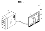
- FIG. 1 A liquid crystal display (“LCD”) according to an exemplary embodiment of the present invention and a display system including the LCD, according to an exemplary embodiment of the present invention will now be described in further detail with reference to FIG. 1 .
- FIG. 1 is a perspective view of a display system 1 according to an exemplary embodiment of the present invention.
- the display system 1 includes an LCD 11 and a central processing device 15.
- the LCD 11 provides a substantially improved, e.g., easy and convenient, interface to a user. Specifically, when the user touches a liquid crystal panel 400 ( FIG. 2 ) of the LCD 11 with a pen PEN, the LCD 11 outputs touch position information to the central processing device 15. In addition, the LCD 11 recognizes the shape of an object OB disposed proximate to the liquid crystal panel 400, and outputs object shape information regarding the object OB to the central processing device 15. More specifically, the LCD 11 recognizes the shape of the object OB disposed on the liquid crystal panel 400 using a sensing signal SIG ( FIG. 5 ).
- SIG sensing signal
- the sensing signal SIG includes infrared rays or, alternatively, ultrasonic waves for example, but alternative exemplary embodiments are not limited thereto.
- the LCD 11 emits the sensing signal SIG toward a front of the liquid crystal panel 400, and detects the sensing signal SIG reflected from the object OB, thereby determining a shape of the object OB, as will be described in further detail below.
- the central processing device 15 performs signal processing on touch position information and/or the object shape information provided by the LCD 11.
- the central processing device 15 is a computer, but alternative exemplary embodiments are not limited thereto.
- the LCD 11 includes the liquid crystal panel 400, a backlight unit including a plurality of light sources which emit light and/or the sensing signal SIG, and a plurality of sensors disposed on a rear surface of the liquid crystal panel 400 and which recognize the shape of the object OB by detecting infrared rays, for example, reflected from the object OB.
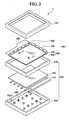
- FIG. 2 is an exploded perspective view of the LCD 11 according to an exemplary embodiment of the present invention
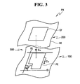
- FIG. 3 is an equivalent circuit diagram of a pixel of the LCD 11 according to an exemplary embodiment of the present invention
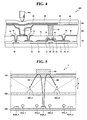
- FIG. 4 is a partial cross-sectional view of the liquid crystal panel 400 taken along line IV-IV' of FIG. 2
- FIG. 5 is a partial cross-sectional view of the LCD 11 taken along line IV-IV' of FIG. 2 .
- the LCD 11 includes a liquid crystal panel assembly 500, a backlight unit 600 and a top chassis 700.
- the liquid crystal panel assembly 500 includes the liquid crystal panel 400, a gate driver 510, a data driver 520 and a circuit board 530.
- the liquid crystal panel 400 includes a first display panel 100, a second display panel 200 and a liquid crystal layer (not shown) interposed between the first display panel 100 and the second display panel 200.
- a plurality of gate lines (not shown), a plurality of data lines (not shown) and a plurality of pixel electrodes (not shown) are formed on the first display panel 100.
- a common electrode (not shown) is formed on the second display panel 200.
- Each pixel (not shown) includes a pixel electrode PE ( FIG. 3 ) and a common electrode CE ( FIG 3 ) which is disposed opposite to, e.g., faces, the pixel electrode PE.
- a pixel PX is connected to an i-th gate line Gi and a j-th data line Dj, and includes a switching device Qp connected to the i-th gate line Gi and the j-th data line Dj, as well as a liquid crystal capacitor C 1c and a storage capacitor C st , which are both connected to the switching device Qp.
- the liquid crystal capacitor C 1c includes the pixel electrode PE, formed on the first display panel 100, and the common electrode CE formed on the second display panel 200, as shown in FIG. 3 .
- a color filter CF is formed on the common electrode CE.
- the liquid crystal panel 400 includes a plurality of the pixels PX and displays an image.
- the liquid crystal panel 400 according to an exemplary embodiment recognizes, e.g., determines, a position of a touch, e.g., an external pressure, on the liquid crystal panel 400.
- the liquid crystal panel 400 will be described in further detail below with reference to FIG. 4 .
- the gate driver 510 and/or the data driver 520 may be attached to the liquid crystal panel 400 by being mounted on a flexible printed circuit film (not shown) as a tape carrier package ("TCP").
- TCP tape carrier package
- the gate driver 510 and/or the data driver 520 may be integrated on the liquid crystal panel 400 along with the plurality of gate lines, the plurality of data lines, and the switching devices Qp of each of the pixels PX.
- the gate driver 510 applies a gate signal to the plurality of gate lines.
- the gate signal may be obtained by combining a gate-on voltage and a gate-off voltage, provided by a gate-on/off voltage generation module (not shown).
- the data driver 520 applies an image data voltage to the data lines.
- a plurality of circuits for generating a gate control signal for controlling an operation of the gate driver 510, as well as a plurality of circuits for generating a data control signal for controlling the operation of the data driver 520, may be mounted on the circuit board 530.
- a timing controller (not shown) may be mounted on the circuit board 530, but alternative exemplary embodiments are not limited thereto.
- the liquid crystal panel assembly 500 is disposed above the backlight unit 600 and is provided with light by the backlight unit 600 to display an image thereon.
- the backlight unit 600 includes a side member 630, a first diffusion member 620, a plurality of first light sources 610, each first light source 610 of which emits light, a plurality of second light sources IRLED, each second light source IRLED of which emits a sensing signal SIG, and a plurality of sensors SEN.
- the side member 630 supports the liquid crystal panel assembly 500, and contains the first diffusion member 620, the first light sources 610, the second light sources IRLED and the sensors SEN therein. Inner surfaces of the side member 630 reflect light emitted from the first light sources 610 and the sensing signal SIG emitted the second light sources IRLED. Alternatively, a reflective plate (not shown) may be attached the inner surfaces of the side member 630.
- a first diffusion member 620 is disposed above the first light sources 610.
- the first diffusion member 620 improves a uniformity of a luminance of light emitted from the first light sources 610.
- the first light sources 610 are disposed at a rear portion of the liquid crystal panel 400, and emit light.
- the first light sources 610 may be cold cathode fluorescent lamps ("CCFLs"), external electrode fluorescent lamps (“EEFLs”) or, alternatively, hot cathode fluorescent lamps (“HCFLs”).
- the first light sources 610 may be light-emitting diodes ("LEDs").
- the first light sources 610 may emit infrared rays, as well as visible rays, but alternative exemplary embodiments are not limited thereto.
- the second light sources IRLED are disposed at the rear portion of the liquid crystal panel 400 and emit the sensing signal SIG.
- the sensing signal SIG includes infrared rays and/or ultrasonic waves.
- infrared rays are light having a long wavelength, e.g., a wavelength of approximately 0.75 ⁇ m or greater.
- Infrared rays may be used to recognize the shape of the object OB, which is disposed at a front portion of the liquid crystal panel 400, e.g., outside of the liquid crystal panel 400.
- the infrared rays according to an exemplary embodiment of the present invention have a wavelength sufficient to transmit through the liquid crystal panel 400.
- a portion of the infrared rays transmitted through the liquid crystal panel 400 reach the object OB and are reflected from the object OB back toward the second light sources IRLED.
- the first light sources 610 and the second light sources IRLED are separate light sources, but alternative exemplary embodiments of the present invention are not limited thereto.
- the first light sources 610 and the second light sources IRLED may be incorporated into single light sources (not shown) which emit both light and the sensing signal SIG.
- the first light sources 610 and the second light sources IRLED may be mounted on a same board, e.g., a same circuit board in the LCD 11, and may further be mounted on a bottom chassis 640 of the LCD 11, as shown in FIG. 2 .
- the sensors SEN are disposed at the rear portion of the liquid crystal panel 400, detect the sensing signal SIG reflected from the object OB, and thus determine a shape of the object OB ( FIG. 1 ).
- the sensors SEN may be infrared sensors. Further, the sensors SEN may output object shape information regarding the object OB to the central processing device 15 ( FIG. 1 ).
- An exemplary embodiment of the present invention includes a plurality of the sensors SEN, as shown in FIG. 2 . Thus, a number and arrangement of the sensors SEN may vary based on a sensitivity of the sensors SEN, for example.
- the bottom chassis 640 of the LCD 11 contains the side member 630, the first diffusion member 620, the first light sources 610, the second light sources IRLED and the sensors SEN therein.
- the bottom chassis 640 and the top chassis 700 contain the light crystal panel assembly 500 and the backlight unit 600 therebetween.
- the top chassis 700 is coupled to, e.g., is connected to, the bottom chassis 640 with hooks (not shown) or, alternatively, with screws (not shown), but alternative exemplary embodiments are not limited thereto.
- the liquid crystal panel 400 may be a touch screen which detects a position of a touch, e.g., an external pressure applied by a user, for example, thereon.
- the liquid crystal panel 400 will now be described in further detail with reference to FIG. 4 .
- the touch screen panel may be classified as a capacitive touch screen panel, a resistive touch screen panel and a surface ultrasonic wave touch screen panel, for example.
- a resistive touch screen panel will hereinafter be described, but alternative exemplary embodiments of the present invention are not limited thereto.
- a gate electrode 26 is formed on an insulating substrate 10 of the liquid crystal panel 400 according to an exemplary embodiment of the present invention.
- a first touch sensor electrode 29 is formed on the insulating substrate 10 as a protrusion therefrom and is spaced apart from the gate electrode 26, as shown in FIG. 4 .
- the first touch sensor electrode 29 is a terminal of a touch sensor and is connected to a first touch sensor pad 84 through a contact hole 72.
- the first touch sensor electrode 29 is electrically connected to a common electrode 90 on a touch sensor spacer 92, and thus provides touch position information to the central processing device 15 ( FIG. 1 ).
- a gate insulation layer 30 is formed of silicon nitride ("SiNx”), for example, on the gate electrode 26 and the first touch sensor electrode 29.
- a semiconductor layer 40 is formed of hydrogenated amorphous silicon or polycrystalline silicon, for example, on the gate insulation layer 30.
- Resistive contact layers 55 and 56 are formed of silicide or n+ hydrogenated amorphous silicon, for example, which is doped with a high concentration of n-type impurities, on the semiconductor layer 40.
- a data line 62 and a drain electrode 66 are formed on the resistive contact layers 55 and 56 and the gate insulation layer 30, as shown in FIG. 4 .
- a source electrode 65 extends from the data line 62 and over a portion of the semiconductor layer 40.
- the drain electrode 66 is spaced apart from the source electrode 65 and is disposed above the semiconductor layer 40. Further, the source electrode 65 and the drain electrode 66 are disposed on opposite sides of the gate electrode 26 above the semiconductor layer 40.
- the gate electrode 26, the source electrode 65 and the drain electrode 66 form a switching device, e.g., a thin film transistor such as the switching device Qp ( FIG. 3 ).
- the drain electrode 66 may include a bar-shaped pattern, e.g., a rectangular-shaped pattern, which extends over a portion of the semiconductor layer 40, as well as a drain electrode expanded portion 67, which has a wider area than an area of the bar-shaped pattern and above which a contact hole 76 is formed through a passivation layer 70.
- a bar-shaped pattern e.g., a rectangular-shaped pattern
- a drain electrode expanded portion 67 which has a wider area than an area of the bar-shaped pattern and above which a contact hole 76 is formed through a passivation layer 70.
- a second touch sensor electrode 63 is formed on the gate insulation layer 30.
- the second touch sensor electrode 63 is a terminal of a touch sensor and is connected to a second touch sensor pad 85 through a contact hole 73.
- the second touch sensor electrode 63 is electrically connected to the common electrode 90 on the touch sensor spacer 92, and thus provides touch position information.
- the first touch sensor electrode 29 provides a row-direction coordinate of a touch position
- the second touch sensor electrode 63 provides a column-direction coordinate of the touch position, but alternative exemplary embodiments of the present invention are not limited thereto.
- the passivation layer 70 is formed on the source electrode 65, the drain electrode 66 and the second touch sensor electrode 63, as shown in FIG. 4 .
- a pixel electrode 82 is formed on the passivation layer 70, and is electrically connected to the drain electrode 66 through the contact hole 76.
- the pixel electrode 82 to which an image data voltage is applied, generates an electric field along with the common electrode 90 and thus determines a alignment of liquid crystal molecules (not shown) in a liquid crystal layer 300 between the pixel electrode 82 and the common electrode 90.
- the first touch sensor pad 84 and the second touch sensor pad 85 are formed on the passivation layer 70.
- the first touch sensor pad 84 is connected to the first touch sensor electrode 29 through the contact hole 72
- the second touch sensor pad 85 is connected to the second touch sensor electrode 63 through the contact hole 73.
- a black matrix 94 and a color filter 98 are formed on an insulating substrate 96.
- the color filter 98 includes as a red color filter 89, a green color filter 98 and/or a blue color filter 98.
- the black matrix 94 prevents light leakage through the liquid crystal panel 400.
- the touch sensor spacer 92 is formed on the black matrix 94, as shown in FIG. 4 .
- the common electrode 90 is formed of a transparent conductive material such as indium tin oxide ("ITO”) or indium zinc oxide (“IZO”) on the black matrix 94, the color filter 98 and the touch sensor spacer 92.
- ITO indium tin oxide
- IZO indium zinc oxide
- a supporting spacer 93 is formed on the common electrode 90.
- the supporting spacer 93 supports the first display panel 100 and the second display panel 200 and thus maintains a uniform cell gap between the first display panel 100 and the second display panel 200.
- the touch sensor spacer 92 is separate from the first display panel 100. However, when the external pressure is applied, the common electrode 90 on the touch sensor spacer 92 contacts and electrically connects to the first touch sensor pad 84 and the second touch sensor pad 85, as shown in FIG. 4 . As a result, the LCD 11 recognizes a touch position, and outputs the touch position information to a central processing device 15 ( FIG. 1 ).
- first light sources 610_1 through 610_4 second light sources IRLED_1 through IRLED_3 and sensors SEN_1 and SEN_2 are disposed below the liquid crystal panel 400.
- the first light sources 610_1 through 610_4 are disposed below the liquid crystal panel 400 and provide light to the liquid crystal panel 400.
- the first diffusion member 620 is disposed between the liquid crystal panel 400 and the first light sources 610_1 through 610_4, and improves a uniformity of a luminance of light emitted therefrom.
- the second light sources IRLED_L through IRLED_3 are disposed below the liquid crystal panel, and more specifically, are disposed below the first diffusion member 620, as shown in FIG. 5 .
- the second light sources IRLED_1 through IRLED_3 emit the sensing signal SIG toward the liquid crystal panel 400, e.g., upward in FIG. 5 , to recognize the shape of the object OB.
- the sensing signal SIG emitted by the second light sources IRLED_1 through IRLED_3 transmits through the liquid crystal panel 400, reaches the object OB, and is reflected from the object OB back toward the second light sources IRLED_1 through IRLED_3.
- the sensors SEN_1 and SEN_2 are disposed on the first diffusion member 620 below the liquid crystal panel 400.
- the sensors SEN_1 and SEN_2 detect the sensing signal SIG reflected from the object OB before the reflected sensing signal SIG transmits through or is absorbed by the first diffusion member 620. Therefore, an efficiency of detection of the sensing signal SIG is substantially increased in an LCD 11 according to an exemplary embodiment of the present invention.
- the sensors SEN_1 and SEN_2 recognize a shape of the object OB by detecting the sensing signal SIG reflected from the object OB, and output object shape information regarding the object OB to central processing device 15 ( FIG. 1 ).
- An arrangement and positions of the sensors SEN_1 and SEN_2, as well as a depth D of the sensors SEN_1 and SEN_2, is determined based on a viewing angle ⁇ of the sensors SEN_1 and SEN2. Specifically, as the depth D of the sensors SEN_1 and SEN_2 increases, the sensors SEN_1 and SEN_2 become less visible from above the liquid crystal panel 400, but the sensitivity of the sensors SEN_1 and SEN_2 decreases.
- the depth D is determined based upon sensitivities of the sensors SEN_1 and SEN_2 and the viewing angle ⁇ . As shown in FIG. 5 , the depth D represents a distance between the sensors SEN_1 and SEN_2 and a member, e.g., the first diffusion member 620, disposed directly above the sensors SEN_1 and SEN2. In an exemplary embodiment of the present invention, the depth D is less than or equal to approximately 100 mm.
- Each of the sensors SEN_1 and SEN_2 may include an infrared filter (not shown), which detects infrared rays.
- the sensors SEN_1 and SEN2 detect infrared rays having a long wavelength, e.g., a wavelength of approximately 700 nm or more, with the infrared filters.
- the LCD 11 according to an exemplary embodiment of the present invention functions as both a touch screen panel, which can detect a position of a touch on the liquid crystal panel 400, as well as determining a shape of an object OB on the liquid crystal panel 400. Therefore, the LCD 11 according to an exemplary embodiment provides an easy and convenient interface to a user.
- alternative exemplary embodiments of the present invention are not limited to the abovementioned examples. Instead, the LCD 11 according to an alternative exemplary embodiment may include only one of a touch screen function and a shape recognition function. Put another way, the LCD 11 according to an alternative exemplary embodiment recognizes a shape of an object OB on the liquid crystal panel 400, but may not necessarily be a touch screen panel.
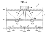
- FIG. 6 is a partial cross-sectional view of an LCD 12 according to an alternative exemplary embodiment of the present invention.
- the same reference numerals indicate the same or like elements, and thus, any repetitive detailed description thereof will be omitted.
- the exemplary embodiment shown in FIG. 6 will hereinafter be described in further detail, to describe differences between the exemplary embodiment shown in FIG. 6 and the exemplary embodiment shown in FIG. 5 .
- one or more holes are formed through a first diffusion member 621, and sensors SEN_1 and SEN_2 are inserted into corresponding holes H_1 and H_2. Therefore, the sensors SEN_1 and SEN_2 detect the sensing signal SIG reflected from an object OB away from the LC panel 400 and back toward the sensors SEN_1 and SEN_2 before the sensing signal SIG transmits through or is absorbed by the first diffusion member 621.
- a size of each of the holes H_1 and H_2 is determined such that the holes H_1 and H_2 are not visible from a viewing position outside, e.g., above, the liquid crystal panel 400. Further, the size of each of the holes H_1 and H_2 may be determined by a size of the sensors SEN_1 and SEN_2. For example, a diameter of the holes H_1 and H_2 according to an exemplary embodiment of the present invention is approximately 5 mm or less.
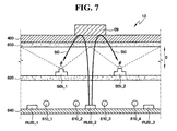
- FIG. 7 is a partial cross-sectional view of an LCD 13 according to another alternative exemplary embodiment of the present invention.
- the same reference numerals indicate the same or like elements, and thus, any repetitive detailed description thereof will be omitted.
- the exemplary embodiment shown in FIG. 7 will hereinafter be described in further detail to describe differences between the exemplary embodiment shown in FIG. 7 and the exemplary embodiment shown in FIG. 5 .
- a second diffusion member 650 is disposed between the liquid crystal panel 400 and the first diffusion member 620. More specifically, the second diffusion member 650 is disposed on a bottom surface of the liquid crystal panel 400, e.g., on a side of the liquid crystal panel 400 closest to the first diffusion member 620, as shown in FIG. 7 .
- the first diffusion member 620 diffuses light emitted from the first light sources 610_1 through 610_4 and thus provides the light to the liquid crystal panel 400. In addition, the first diffusion member 620 prevents the first light sources 610_1 through 610_4 and the second light sources IRLED_1 through IRLED_3 from being seen from outside, e.g., above, the liquid crystal panel 400.
- the second diffusion member 650 prevents the sensors SEN_1 and SEN2 from being seen from above the liquid crystal panel 400. Further, the second diffusion member 650 diffuses light and provides the light to the liquid crystal panel 400.
- a parallel transmittance of the second diffusion member 650 may be greater than a parallel transmittance of the first diffusion member 620, as will hereinafter be described in further detail with reference to FIG. 8.
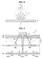
- FIG 8 is a partial cross sectional view of light incident upon a diffusion member which illustrates parallel transmittances according to an exemplary embodiment of the present invention.
- Parallel transmittance is defined as a ratio of a luminance of light emitted through diffusion member, e.g., the first diffusion member 620 or the second diffusion member 650, at an angle within approximately 5 degrees of an incidence direction of the light to a total luminance of all light emitted through the diffusion member. Specifically, referring to FIG.
- a ratio of a luminance T p of the light emitted through the diffusion member M at an angle within approximately 5 degrees of an incidence direction of the light L to a total luminance T t of all light L emitted through the diffusion member M is defined as parallel transmittance.
- the sensing signal SIG (e.g., infrared rays) is reflected from the object OB and is input to, e.g., is sensed by, the sensors SEN_1 and SEN_2 through the second diffusion member 650.
- SIG e.g., infrared rays
- the parallel transmittance of the second diffusion member 650 is too high, the sensors SEN_1 and SEN_2 can be seen from above, e.g., outside, the liquid crystal panel 400, and thus, the parallel transmittance of the second diffusion member 650 according to an exemplary embodiment of the present invention is in a predetermined range, for example, of approximately 25% to - approximately 35%. Further, the parallel transmittance of the second diffusion member 650 in an alternative exemplary embodiment of the present invention may be altered according to the depth D ( FIG. 7 ) and the viewing angle ⁇ ( FIG. 7 ) of the sensors SEN_1 and SEN_2.
- FIG. 9 is a cross-sectional view of an LCD 14 according to another exemplary embodiment of the present invention.
- the same reference numerals indicate the same or like elements, and thus, any repetitive detailed description thereof will be omitted.
- the exemplary embodiment shown FIG. 9 will hereinafter be described in further detail to describe on differences between the exemplary embodiment shown FIG. 9 and the exemplary embodiment shown in FIG. 7 .
- a second diffusion member 650 is disposed on an upper, e.g., a top, surface of the liquid crystal panel 400.
- the second diffusion member 650 prevents the sensors SEN_1 and SEN2 from being seen from above, e.g., from outside, the liquid crystal panel 400.
- the parallel transmittance of the second diffusion member 650 is greater than the parallel transmittance of a first diffusion member 620, as described in greater detail above.
- the parallel transmittance of the second diffusion member 650 may be, for example, in a range of approximately 25% to approximately 35%.
- the parallel transmittance of the second diffusion member 650 may be altered based on the depth D and the viewing angle ⁇ of the sensors SEN_1 and SEN_2.
- FIG. 10 is a partial cross-sectional view of an LCD 15 according to still another alternative exemplary embodiment of the present invention.
- the same reference numerals indicate the same or like elements, and thus, and repetitive detailed description thereof will be omitted.
- the exemplary embodiment shown in FIG. 10 will hereinafter be described in further detail to describe differences between the exemplary embodiment shown in FIG. 10 and the exemplary embodiment shown in FIGS. 6 and 7 .
- a second diffusion member 650 is disposed between the liquid crystal panel 400 and the first diffusion member 620. More specifically, the second diffusion member 650 is disposed on a lower surface, e.g., a bottom surface, of the liquid crystal panel 400. The second diffusion member 650 prevents the sensors SEN_1 and SEN_2 and the holes H_1 and H_2 from being seen from outside, e.g., above, the liquid crystal panel 400.
- the parallel transmittance of the second diffusion member 650 is greater than the parallel transmittance of the first diffusion member 620.
- the parallel transmittance of the second diffusion member 650 may have, for example, a range of approximately 25% to approximately 35%.
- the parallel transmittance of the second diffusion member 650 may be altered, however, according to the depth D and the viewing angle ⁇ of the sensors SEN_1 and SEN_2.
- FIG. 11 is a partial cross-sectional view of an LCD 16 according to another alternative exemplary embodiment of the present invention.
- the same reference numerals indicate the same or like elements, and thus, any repetitive detailed description thereof will be omitted.
- the exemplary embodiment shown in FIG. 11 will hereinafter be described in further detail to describe differences between the exemplary embodiment shown in FIG. 11 and the exemplary embodiment shown in FIG. 10 .
- a second diffusion member 650 is disposed on an upper surface, e.g., a top surface, of the liquid crystal panel 400.
- the second diffusion member 650 prevents the sensors SEN_1 and SEN2 and the holes H_1 and H_2 from being seen from above, e.g., from outside, the liquid crystal panel 400.
- the parallel transmittance of the second diffusion member 650 is greater than the parallel transmittance of the first diffusion member 620.
- the parallel transmittance of the second diffusion member 650 is in a range from approximately 25% to approximately 35%.
- the parallel transmittance of the second diffusion member 650 may be altered based on the depth D and the viewing angle ⁇ of the sensors SEN_1 and SEN_2.
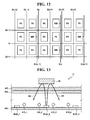
- FIG. 12 a plan view of a liquid crystal panel according to another alternative exemplary embodiment of the present invention
- FIG. 13 is a partial cross-sectional view of an LCD 17 according to still another alternative exemplary embodiment of the present invention.
- the same reference numerals indicate the same or like elements, and thus, any repetitive detailed description thereof will be omitted.
- the exemplary embodiment shown in FIG. 13 will hereinafter be described in further detail to describe differences between the exemplary embodiment shown in FIG. 13 and the exemplary embodiment shown in FIG. 5 .
- a plurality of sensors SEN are disposed in a liquid crystal panel 402.
- the sensors SEN may be disposed in a substantially matrix pattern among a plurality of the pixels PX, as shown in FIG. 12 .
- sensors SEN of the plurality of sensors SEN may be mounted on one of the first display panel 100 ( FIG. 2 ) and the second display panel 200 ( FIG. 2 ) of the liquid crystal panel 402.
- the sensors SEN may be formed on the first display panel 100, on which a thin-film transistor ("TFT") array is formed, along with the switching devices Qp ( FIG. 3 ) of the pixels PX.
- TFT thin-film transistor
- the sensing signal SIG emitted from the second light sources IRLED_1 through IRLED_3 is reflected back toward the second light sources IRLED_1 through IRLED_3 by an object OB disposed on the liquid crystal panel 402, and a reflected sensing signal SIG is detected by the sensors SEN ( FIG. 12 ) in the liquid crystal panel 402 ( FIG. 13 ).
- the sensors SEN output object shape information regarding the object OB to the central processing device 15 ( FIG. 1 ) through a plurality of sensor lines SL(k-1), SLk and SL(k+1).
- FIGS. 14 through 18 are plan views of a liquid crystal panel which illustrate a method of recognizing an object using an LCD according to an exemplary embodiment of the present invention.
- the exemplary embodiment shown in FIGS. 14 through 18 will hereinafter be described in further detail, using the LCD 11 according to the exemplary embodiment of the present invention shown in FIG. 5 as an example for purposes of illustration only, e.g., methods of recognizing an object using an LCD according to alternative exemplary embodiments of the present invention are not limited to the LCD 11 shown in FIG. 5 .
- the second light sources IRLED_1 through IRLED emit the sensing signal SIG toward the liquid crystal panel 400 in order to recognize the shape of the object OB, which is disposed on the liquid crystal panel 400, e.g., is proximate to the liquid crystal panel 400 outside the liquid crystal panel 400.
- the sensing signal SIG transmits through the liquid crystal panel 400, and is reflected by the object OB away from the liquid crystal panel 400, e.g., is reflected back toward the second light sources IRLED_1 through IRLED_3.
- the reflected sensing signal SIG is detected by the sensors SEN_1 and SEN_2.
- the sensing signal SIG detected by the sensors SEN_1 and SEN2 is subjected to correction, thereby obtaining object shape information regarding the object. Then, the object shape information is output to the central processing unit 15 ( FIG. 1 ).
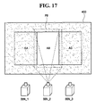
- the liquid crystal panel 400 is divided into a plurality of active regions. Specifically, the liquid crystal panel 400 is divided into a first active region AA, a second active region AB and a third active region AC.
- a plurality of sensors e.g., a first sensor SEN_1, a second sensor SEN_2 and a third sensor SEN_3 corresponding to the first active region ⁇ A, the second active region AB and the third active region AC, respectively, are provided, as described in greater detail above.
- the liquid crystal panel 400 is divided into three active regions, and three sensors are provided, as shown in FIG. 14 .
- alternative exemplary embodiments of the present invention are not limited thereto.
- the first sensor SEN_1 detects a sensing signal (not shown) which transmits through the first active region AA
- the second sensor SEN_2 detects a sensing signal (not shown) which transmits through the second active region AB
- the third sensor SEN_3 detects a sensing signal (not shown) which transmits through the third active region AC.
- a first sensing area PA which is a coverage area of the first sensor SEN_1, includes the first active region AA and is also larger than the first active region AA.
- a second sensing area PB which is a coverage area of the second sensor SEN_2, includes the second active region AB and is likewise larger than the second active region AB.
- a third sensing area PC which is a coverage area of the third sensor SEN_3, includes the third active region AC and is also larger than the third active region AC.
- the first, second and third sensing areas PA, PB and PC respectively, partially overlap one another, as shown in FIG. 14 .
- any redundancy in sensing signals detected by the first, second and/or third sensors SEN_1, SEN_2 and/or SEN_3, respectively, is corrected for in an exemplary embodiment of the present invention. Specifically, only sensing signals regarding the first, second and third active regions AA, AB, and AC, respectively, are extracted from sensing signals based on the first, second and third sensing areas PA, PB and PC, respectively.
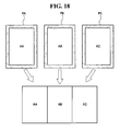
- a first test image such as a white image is displayed in the first active region AA of the liquid crystal panel 400
- a second test image such as a black image is displayed on the whole liquid crystal panel 400 except for the first active region AA.
- the first sensor SEN_1 detects portions of both the first test image and the second test image which fall within the coverage area of the first sensor SEN_1, e.g., the first sensing area PA. Put another way, the first sensor SEN_1 detects the first test image and a portion of the second test image.
- coordinates of the first test image and coordinates of a portion of the second test image which falls within the first sensing area PA are determined.
- the coordinates of the first test image may be substantially the same as coordinates of the first active region AA.
- the second sensor SEN_2 like the first sensor SEN_1, detects portions of the first test image and the second test image which fall within the coverage area of the second sensor SEN_2, e.g., the second sensing area PB.
- the first test image is extracted from the results of the detection performed by each of the first, second and third sensors SEN_1, SEN_2, and SEN_3, respectively, and the extracted first test images are combined, thereby obtaining an image of the first, second and third active regions AA, AB, and AC, respectively.
- the first, second and third sensors SEN_1, SEN_2 and SEN_3, respectively each detect a sensing signal based on the active region AA, a sensing signal regarding the active region AB, and a sensing signal regarding the active region AC, respectively, by using the coordinates of the first test image.
- the first, second and third sensors SEN_1, SEN_2 and SEN_3, respectively each detect a sensing signal regarding the sensing area PA, a sensing signal regarding the sensing area PB, and a sensing signal regarding the sensing area PC, respectively, remove portions of the respective sensing signals corresponding to the coordinates of a second test image, and extract and combine the remaining sensing signals, which correspond to the coordinates of the first test image, thereby providing object shape information for the object OB.
- an LCD provides advantages which include, but are not limited to, a substantially increased efficiency of detection of a sensing signal.
Landscapes
- Engineering & Computer Science (AREA)
- Physics & Mathematics (AREA)
- General Engineering & Computer Science (AREA)
- Nonlinear Science (AREA)
- General Physics & Mathematics (AREA)
- Theoretical Computer Science (AREA)
- Human Computer Interaction (AREA)
- Signal Processing (AREA)
- Multimedia (AREA)
- Mathematical Physics (AREA)
- Chemical & Material Sciences (AREA)
- Optics & Photonics (AREA)
- Crystallography & Structural Chemistry (AREA)
- Liquid Crystal (AREA)
- Devices For Indicating Variable Information By Combining Individual Elements (AREA)
- Control Of Indicators Other Than Cathode Ray Tubes (AREA)
- Position Input By Displaying (AREA)
Applications Claiming Priority (1)
| Application Number | Priority Date | Filing Date | Title |
|---|---|---|---|
| KR20080023847A KR101493840B1 (ko) | 2008-03-14 | 2008-03-14 | 액정 표시 장치, 표시 시스템, 및 액정 표시 장치를 이용한물체 형상의 인식 방법 |
Publications (2)
| Publication Number | Publication Date |
|---|---|
| EP2101251A2 true EP2101251A2 (fr) | 2009-09-16 |
| EP2101251A3 EP2101251A3 (fr) | 2011-08-03 |
Family
ID=40513765
Family Applications (1)
| Application Number | Title | Priority Date | Filing Date |
|---|---|---|---|
| EP09001470A Withdrawn EP2101251A3 (fr) | 2008-03-14 | 2009-02-04 | Affichage à cristaux liquides, système d'affichage incluant l'affichage à cristaux liquides et procédé de reconnaissance d'un objet utilisant l'affichage à cristaux liquides |
Country Status (5)
| Country | Link |
|---|---|
| US (1) | US8189128B2 (fr) |
| EP (1) | EP2101251A3 (fr) |
| JP (2) | JP2009223317A (fr) |
| KR (1) | KR101493840B1 (fr) |
| CN (1) | CN101533170B (fr) |
Cited By (5)
| Publication number | Priority date | Publication date | Assignee | Title |
|---|---|---|---|---|
| EP2511802A1 (fr) * | 2011-04-15 | 2012-10-17 | Research In Motion Limited | Écran tactile avec capteur optique et procédé optique |
| EP2416208A3 (fr) * | 2010-08-06 | 2013-01-02 | Daniel Barthels | Ecran et procédé de représentation de contenus optiques sur un écran |
| US9223431B2 (en) | 2010-09-17 | 2015-12-29 | Blackberry Limited | Touch-sensitive display with depression detection and method |
| US9513737B2 (en) | 2010-09-17 | 2016-12-06 | Blackberry Limited | Touch-sensitive display with optical sensor and method |
| EP3291074A4 (fr) * | 2016-06-30 | 2018-09-19 | Boe Technology Group Co. Ltd. | Écran d'affichage, son procédé de fabrication et dispositif d'affichage |
Families Citing this family (32)
| Publication number | Priority date | Publication date | Assignee | Title |
|---|---|---|---|---|
| US7990481B2 (en) * | 2006-10-30 | 2011-08-02 | Samsung Electronics Co., Ltd. | Display device having particular touch sensor protrusion facing sensing electrode |
| KR101073285B1 (ko) * | 2008-12-01 | 2011-10-12 | 삼성모바일디스플레이주식회사 | 터치 스크린 패널 |
| JP2012027511A (ja) * | 2009-04-23 | 2012-02-09 | Univ Of Tsukuba | 入力装置 |
| CN102063221A (zh) * | 2009-11-17 | 2011-05-18 | 北京汇冠新技术股份有限公司 | 一种交互式显示屏及交互式投影屏幕 |
| US8384694B2 (en) * | 2009-11-17 | 2013-02-26 | Microsoft Corporation | Infrared vision with liquid crystal display device |
| US20110181587A1 (en) * | 2010-01-22 | 2011-07-28 | Sony Corporation | Image display device having imaging device |
| KR101698454B1 (ko) * | 2010-10-22 | 2017-01-23 | 삼성디스플레이 주식회사 | 광원 어셈블리 및 그를 포함하는 터치 스크린 장치 |
| KR101726597B1 (ko) * | 2010-12-13 | 2017-04-14 | 삼성전자주식회사 | 멀티터치 및 근접한 오브젝트 센싱이 가능한 디스플레이 장치 |
| KR20120080845A (ko) * | 2011-01-10 | 2012-07-18 | 삼성전자주식회사 | 광 감지 기능을 구비한 oled 디스플레이 장치 |
| CN102693050A (zh) * | 2011-03-23 | 2012-09-26 | 上海优熠电子科技有限公司 | 具有触摸点形状识别功能的触摸屏 |
| DE112012002330A5 (de) * | 2011-05-31 | 2014-03-20 | Mechaless Systems Gmbh | Display mit integriertem optischen Sender |
| KR20130021214A (ko) * | 2011-08-22 | 2013-03-05 | 삼성디스플레이 주식회사 | 표시 장치 및 이의 제조 방법 |
| MY170979A (en) * | 2012-02-02 | 2019-09-23 | Qualcomm Inc | Ultrasonic touch sensor with a display monitor |
| US9977514B1 (en) | 2012-12-06 | 2018-05-22 | Richard Martin Greene | Method and apparatus for digital painting with natural textures |
| KR102045808B1 (ko) * | 2012-12-13 | 2019-11-18 | 엘지디스플레이 주식회사 | 터치센서 일체형 표시장치 |
| CN103150063A (zh) * | 2013-04-09 | 2013-06-12 | 北京紫霄科技有限公司 | 一种基于lcd的光学多点触控设备 |
| US10036734B2 (en) | 2013-06-03 | 2018-07-31 | Snaptrack, Inc. | Ultrasonic sensor with bonded piezoelectric layer |
| US9551783B2 (en) * | 2013-06-03 | 2017-01-24 | Qualcomm Incorporated | Display with backside ultrasonic sensor array |
| US20140355387A1 (en) | 2013-06-03 | 2014-12-04 | Qualcomm Incorporated | Ultrasonic receiver with coated piezoelectric layer |
| US9465429B2 (en) * | 2013-06-03 | 2016-10-11 | Qualcomm Incorporated | In-cell multifunctional pixel and display |
| CN104516560B (zh) * | 2013-09-27 | 2019-02-05 | 联想(北京)有限公司 | 一种识别方法、装置及电子设备 |
| US10478858B2 (en) | 2013-12-12 | 2019-11-19 | Qualcomm Incorporated | Piezoelectric ultrasonic transducer and process |
| KR102279707B1 (ko) * | 2013-12-18 | 2021-07-22 | 삼성디스플레이 주식회사 | 표시 장치 |
| CN104656305A (zh) * | 2015-03-09 | 2015-05-27 | 京东方科技集团股份有限公司 | 一种彩膜显示层、显示面板及制备方法 |
| CN105445992A (zh) * | 2015-12-02 | 2016-03-30 | 小米科技有限责任公司 | 液晶显示组件及电子设备 |
| CN105739792A (zh) * | 2016-01-22 | 2016-07-06 | 广州华欣电子科技有限公司 | 一种触摸物特征识别方法、触摸屏操作方法及装置 |
| KR101849588B1 (ko) * | 2016-05-30 | 2018-04-17 | 엘지디스플레이 주식회사 | 터치 센서를 가지는 컬러 필터 어레이 및 이를 구비하는 표시 패널 |
| US11003884B2 (en) | 2016-06-16 | 2021-05-11 | Qualcomm Incorporated | Fingerprint sensor device and methods thereof |
| CN107564446A (zh) * | 2017-09-30 | 2018-01-09 | 深圳市华星光电半导体显示技术有限公司 | 一种面板点灯机、面板点灯测试系统及测试方法 |
| CN109799635A (zh) * | 2019-01-16 | 2019-05-24 | 柳州阜民科技有限公司 | 一种电子设备 |
| CN109814297A (zh) * | 2019-03-06 | 2019-05-28 | 武汉华星光电技术有限公司 | 一种阵列基板及显示装置 |
| JP2022549600A (ja) | 2019-09-24 | 2022-11-28 | ベーア-ヘラー サーモコントロール ゲーエムベーハー | 光学式近接センサシステム内蔵の表示装置 |
Family Cites Families (23)
| Publication number | Priority date | Publication date | Assignee | Title |
|---|---|---|---|---|
| JPH0575786A (ja) | 1991-09-13 | 1993-03-26 | Fuji Xerox Co Ltd | 完全密着型イメージセンサ |
| JPH06342146A (ja) * | 1992-12-11 | 1994-12-13 | Canon Inc | 画像表示装置、半導体装置及び光学機器 |
| KR0163895B1 (ko) * | 1995-01-06 | 1999-01-15 | 김광호 | 시야각을 개선한 액정표시장치 |
| US6243069B1 (en) | 1997-04-22 | 2001-06-05 | Matsushita Electric Industrial Co., Ltd. | Liquid crystal display with image reading function, image reading method and manufacturing method |
| JP2000259346A (ja) | 1999-03-12 | 2000-09-22 | Casio Comput Co Ltd | 情報処理装置、入出力装置及び入出力素子 |
| JP2000311048A (ja) * | 1999-04-27 | 2000-11-07 | Matsushita Electric Ind Co Ltd | 操作装置 |
| JP4032661B2 (ja) * | 2000-12-07 | 2008-01-16 | セイコーエプソン株式会社 | 液晶装置および電子機器 |
| KR20020060626A (ko) | 2001-01-10 | 2002-07-18 | 김용선 | 원격형상 실시간 구현 시스템 |
| US6678026B2 (en) * | 2001-04-10 | 2004-01-13 | Seiko Epson Corporation | Liquid crystal device and electronic apparatus |
| JP4141847B2 (ja) * | 2003-01-06 | 2008-08-27 | Smk株式会社 | 操作パネル入力装置 |
| KR20060016518A (ko) * | 2004-08-18 | 2006-02-22 | 삼성전자주식회사 | 표시장치 |
| KR101085447B1 (ko) * | 2004-12-31 | 2011-11-21 | 삼성전자주식회사 | 터치 위치 검출 장치 및 이의 터치 위치 검출 방법과,이를 구비한 터치 스크린 표시 장치 |
| JP2006251395A (ja) * | 2005-03-10 | 2006-09-21 | Daicel Chem Ind Ltd | 異方性散乱シート |
| JP4645822B2 (ja) * | 2005-04-19 | 2011-03-09 | ソニー株式会社 | 画像表示装置および物体の検出方法 |
| WO2007026462A1 (fr) | 2005-08-30 | 2007-03-08 | Sharp Kabushiki Kaisha | Dispositif d’affichage à cristaux liquides |
| JP2007156757A (ja) * | 2005-12-02 | 2007-06-21 | Sharp Corp | 表示装置 |
| JP2007187753A (ja) * | 2006-01-11 | 2007-07-26 | Sharp Corp | 液晶表示装置 |
| US7515143B2 (en) * | 2006-02-28 | 2009-04-07 | Microsoft Corporation | Uniform illumination of interactive display panel |
| JP4891666B2 (ja) * | 2006-06-22 | 2012-03-07 | 東芝モバイルディスプレイ株式会社 | 液晶表示装置 |
| KR101251543B1 (ko) * | 2006-09-01 | 2013-04-08 | 삼성디스플레이 주식회사 | 액정 표시 장치 및 이의 구동 방법과 제조 방법 |
| US8094129B2 (en) | 2006-11-27 | 2012-01-10 | Microsoft Corporation | Touch sensing using shadow and reflective modes |
| US7924272B2 (en) * | 2006-11-27 | 2011-04-12 | Microsoft Corporation | Infrared sensor integrated in a touch panel |
| JP4867766B2 (ja) * | 2007-04-05 | 2012-02-01 | セイコーエプソン株式会社 | 液晶装置、イメージセンサ、及び電子機器 |
-
2008
- 2008-03-14 KR KR20080023847A patent/KR101493840B1/ko not_active Expired - Fee Related
- 2008-10-01 US US12/243,574 patent/US8189128B2/en not_active Expired - Fee Related
-
2009
- 2009-02-04 EP EP09001470A patent/EP2101251A3/fr not_active Withdrawn
- 2009-03-05 CN CN2009101266213A patent/CN101533170B/zh not_active Expired - Fee Related
- 2009-03-16 JP JP2009062688A patent/JP2009223317A/ja active Pending
-
2014
- 2014-03-07 JP JP2014045491A patent/JP2014130374A/ja active Pending
Cited By (6)
| Publication number | Priority date | Publication date | Assignee | Title |
|---|---|---|---|---|
| EP2416208A3 (fr) * | 2010-08-06 | 2013-01-02 | Daniel Barthels | Ecran et procédé de représentation de contenus optiques sur un écran |
| US9223431B2 (en) | 2010-09-17 | 2015-12-29 | Blackberry Limited | Touch-sensitive display with depression detection and method |
| US9513737B2 (en) | 2010-09-17 | 2016-12-06 | Blackberry Limited | Touch-sensitive display with optical sensor and method |
| EP2511802A1 (fr) * | 2011-04-15 | 2012-10-17 | Research In Motion Limited | Écran tactile avec capteur optique et procédé optique |
| EP3291074A4 (fr) * | 2016-06-30 | 2018-09-19 | Boe Technology Group Co. Ltd. | Écran d'affichage, son procédé de fabrication et dispositif d'affichage |
| US10311277B2 (en) | 2016-06-30 | 2019-06-04 | Boe Technology Group Co., Ltd. | Display panel and method of manufacturing the same, and display apparatus |
Also Published As
| Publication number | Publication date |
|---|---|
| KR101493840B1 (ko) | 2015-02-17 |
| US8189128B2 (en) | 2012-05-29 |
| US20090231497A1 (en) | 2009-09-17 |
| JP2009223317A (ja) | 2009-10-01 |
| KR20090098446A (ko) | 2009-09-17 |
| EP2101251A3 (fr) | 2011-08-03 |
| CN101533170B (zh) | 2013-02-13 |
| CN101533170A (zh) | 2009-09-16 |
| JP2014130374A (ja) | 2014-07-10 |
Similar Documents
| Publication | Publication Date | Title |
|---|---|---|
| US8189128B2 (en) | Liquid crystal display having first and second diffusion members and a plurality of sensors that can detect a sensing signal reflected from an object | |
| US8743063B2 (en) | Liquid crystal display with integrated touch screen panel | |
| CN101673013B (zh) | 包括触摸面板的液晶显示器件 | |
| US8269940B2 (en) | Sensing structure | |
| US9495030B2 (en) | Liquid crystal display device comprising touch screen | |
| TWI399582B (zh) | 液晶顯示裝置 | |
| US9058076B2 (en) | Touch panel | |
| TWI417766B (zh) | 觸控液晶顯示裝置及其驅動方法 | |
| US8427448B2 (en) | Liquid crystal display | |
| US7692729B2 (en) | Liquid crystal display including sensing unit | |
| US10996498B2 (en) | Display apparatus with touch sensing and force sensing functions | |
| US20120044171A1 (en) | Liquid crystal display integrated touch screen panel | |
| US20120206396A1 (en) | Display device with attached touch panel | |
| US20100328268A1 (en) | Information input device and display device | |
| WO2004090708A1 (fr) | Ecran a surface d'affichage | |
| US10802653B2 (en) | Touch type display device and method for sensing touch thereof | |
| US8698167B2 (en) | Light sensor and display apparatus having the same | |
| US9019221B2 (en) | Display device integrated with touch screen panel | |
| CN101727224B (zh) | 触控式平面显示器及触控方法 | |
| JP2008009225A (ja) | 表示装置及びその製造方法 | |
| KR20230133441A (ko) | 디스플레이 일체형 터치 검출 장치 | |
| KR20180076018A (ko) | 터치 방식 표시장치 |
Legal Events
| Date | Code | Title | Description |
|---|---|---|---|
| PUAI | Public reference made under article 153(3) epc to a published international application that has entered the european phase |
Free format text: ORIGINAL CODE: 0009012 |
|
| AK | Designated contracting states |
Kind code of ref document: A2 Designated state(s): AT BE BG CH CY CZ DE DK EE ES FI FR GB GR HR HU IE IS IT LI LT LU LV MC MK MT NL NO PL PT RO SE SI SK TR |
|
| AX | Request for extension of the european patent |
Extension state: AL BA RS |
|
| PUAL | Search report despatched |
Free format text: ORIGINAL CODE: 0009013 |
|
| AK | Designated contracting states |
Kind code of ref document: A3 Designated state(s): AT BE BG CH CY CZ DE DK EE ES FI FR GB GR HR HU IE IS IT LI LT LU LV MC MK MT NL NO PL PT RO SE SI SK TR |
|
| AX | Request for extension of the european patent |
Extension state: AL BA RS |
|
| RIC1 | Information provided on ipc code assigned before grant |
Ipc: H04N 1/195 20060101ALI20110630BHEP Ipc: G02F 1/13357 20060101ALI20110630BHEP Ipc: G02F 1/133 20060101ALI20110630BHEP Ipc: G06F 3/042 20060101AFI20110630BHEP |
|
| 17P | Request for examination filed |
Effective date: 20120201 |
|
| AKX | Designation fees paid |
Designated state(s): DE FR GB IT |
|
| RAP1 | Party data changed (applicant data changed or rights of an application transferred) |
Owner name: SAMSUNG ELECTRONICS CO., LTD. |
|
| RAP1 | Party data changed (applicant data changed or rights of an application transferred) |
Owner name: SAMSUNG DISPLAY CO., LTD. |
|
| RAP1 | Party data changed (applicant data changed or rights of an application transferred) |
Owner name: SAMSUNG DISPLAY CO., LTD. |
|
| STAA | Information on the status of an ep patent application or granted ep patent |
Free format text: STATUS: THE APPLICATION IS DEEMED TO BE WITHDRAWN |
|
| 18D | Application deemed to be withdrawn |
Effective date: 20170901 |