EP2101554B1 - Boîtier doté d'une platine conductrice - Google Patents
Boîtier doté d'une platine conductrice Download PDFInfo
- Publication number
- EP2101554B1 EP2101554B1 EP20090405030 EP09405030A EP2101554B1 EP 2101554 B1 EP2101554 B1 EP 2101554B1 EP 20090405030 EP20090405030 EP 20090405030 EP 09405030 A EP09405030 A EP 09405030A EP 2101554 B1 EP2101554 B1 EP 2101554B1
- Authority
- EP
- European Patent Office
- Prior art keywords
- circuit board
- printed circuit
- housing
- connecting ring
- partition wall
- Prior art date
- Legal status (The legal status is an assumption and is not a legal conclusion. Google has not performed a legal analysis and makes no representation as to the accuracy of the status listed.)
- Ceased
Links
- 238000005192 partition Methods 0.000 claims description 68
- 238000004519 manufacturing process Methods 0.000 claims description 13
- 229910052751 metal Inorganic materials 0.000 claims description 13
- 239000002184 metal Substances 0.000 claims description 13
- 229910052782 aluminium Inorganic materials 0.000 claims description 10
- XAGFODPZIPBFFR-UHFFFAOYSA-N aluminium Chemical compound [Al] XAGFODPZIPBFFR-UHFFFAOYSA-N 0.000 claims description 10
- 150000001875 compounds Chemical class 0.000 claims description 9
- RYGMFSIKBFXOCR-UHFFFAOYSA-N Copper Chemical compound [Cu] RYGMFSIKBFXOCR-UHFFFAOYSA-N 0.000 claims description 5
- 229910052802 copper Inorganic materials 0.000 claims description 5
- 239000010949 copper Substances 0.000 claims description 5
- 239000004411 aluminium Substances 0.000 claims 1
- 238000004382 potting Methods 0.000 claims 1
- 230000000284 resting effect Effects 0.000 claims 1
- 238000005266 casting Methods 0.000 description 12
- 238000007142 ring opening reaction Methods 0.000 description 9
- 239000000463 material Substances 0.000 description 6
- 238000000034 method Methods 0.000 description 6
- 239000004020 conductor Substances 0.000 description 5
- 150000002739 metals Chemical class 0.000 description 5
- 230000000694 effects Effects 0.000 description 4
- 230000035939 shock Effects 0.000 description 3
- 238000005476 soldering Methods 0.000 description 3
- 230000007704 transition Effects 0.000 description 3
- XLYOFNOQVPJJNP-UHFFFAOYSA-N water Substances O XLYOFNOQVPJJNP-UHFFFAOYSA-N 0.000 description 3
- 230000009471 action Effects 0.000 description 2
- 238000004026 adhesive bonding Methods 0.000 description 2
- 238000005452 bending Methods 0.000 description 2
- 238000005260 corrosion Methods 0.000 description 2
- 230000007797 corrosion Effects 0.000 description 2
- 230000005670 electromagnetic radiation Effects 0.000 description 2
- 230000002093 peripheral effect Effects 0.000 description 2
- 239000004033 plastic Substances 0.000 description 2
- 229920003023 plastic Polymers 0.000 description 2
- 230000008569 process Effects 0.000 description 2
- 229910000679 solder Inorganic materials 0.000 description 2
- 230000006641 stabilisation Effects 0.000 description 2
- 238000011105 stabilization Methods 0.000 description 2
- 229920000049 Carbon (fiber) Polymers 0.000 description 1
- 241000530268 Lycaena heteronea Species 0.000 description 1
- 230000001133 acceleration Effects 0.000 description 1
- 230000008901 benefit Effects 0.000 description 1
- 239000004917 carbon fiber Substances 0.000 description 1
- 238000006243 chemical reaction Methods 0.000 description 1
- 238000000576 coating method Methods 0.000 description 1
- 230000006835 compression Effects 0.000 description 1
- 238000007906 compression Methods 0.000 description 1
- 238000010276 construction Methods 0.000 description 1
- 238000011109 contamination Methods 0.000 description 1
- 239000000428 dust Substances 0.000 description 1
- 239000011888 foil Substances 0.000 description 1
- 230000007246 mechanism Effects 0.000 description 1
- 239000007769 metal material Substances 0.000 description 1
- 239000012811 non-conductive material Substances 0.000 description 1
- 230000003647 oxidation Effects 0.000 description 1
- 238000007254 oxidation reaction Methods 0.000 description 1
- 238000003825 pressing Methods 0.000 description 1
- 230000003014 reinforcing effect Effects 0.000 description 1
- 230000004044 response Effects 0.000 description 1
- 238000004381 surface treatment Methods 0.000 description 1
- 238000003466 welding Methods 0.000 description 1
Images


Classifications
-
- H—ELECTRICITY
- H05—ELECTRIC TECHNIQUES NOT OTHERWISE PROVIDED FOR
- H05K—PRINTED CIRCUITS; CASINGS OR CONSTRUCTIONAL DETAILS OF ELECTRIC APPARATUS; MANUFACTURE OF ASSEMBLAGES OF ELECTRICAL COMPONENTS
- H05K7/00—Constructional details common to different types of electric apparatus
- H05K7/14—Mounting supporting structure in casing or on frame or rack
- H05K7/1417—Mounting supporting structure in casing or on frame or rack having securing means for mounting boards, plates or wiring boards
- H05K7/142—Spacers not being card guides
-
- H—ELECTRICITY
- H05—ELECTRIC TECHNIQUES NOT OTHERWISE PROVIDED FOR
- H05K—PRINTED CIRCUITS; CASINGS OR CONSTRUCTIONAL DETAILS OF ELECTRIC APPARATUS; MANUFACTURE OF ASSEMBLAGES OF ELECTRICAL COMPONENTS
- H05K7/00—Constructional details common to different types of electric apparatus
- H05K7/14—Mounting supporting structure in casing or on frame or rack
- H05K7/1417—Mounting supporting structure in casing or on frame or rack having securing means for mounting boards, plates or wiring boards
Definitions
- the invention relates to a device comprising a printed circuit board arranged in a housing for an electrical and / or electronic circuit, wherein the printed circuit board has a front region and a rear region. Furthermore, a method for producing a housing with a printed circuit board is the subject of the invention.
- Circuit boards for electronic circuits of electrical or electronic devices are usually placed in a housing to protect them from contamination and mechanical effects.
- the housing also provide protection for the user, as they ensure that the user can not come into contact with the sometimes high voltages on the printed circuit board.
- housings for printed circuit boards are already commercially available in a wide variety of designs. However, most cases are designed for indoor use and have only limited mechanical strength. Although particularly robust housings also exist, these are usually very clumsy and accordingly unwieldy. In addition, the specially robust housing are relatively complicated in construction and production and therefore expensive.
- the US Pat. No. 7,048,564 B1 deals with a sealed electronic module, with a housing open on one side and a printed circuit board equipped with electronic components, which is supported both peripherally and centrally in the housing.
- the printed circuit board has a front and a rear portion, wherein it is mechanically supported in the housing between the front portion and the rear portion.
- the DE 201 15 670 U1 discloses a housing for an electronic control unit in vehicles, with a metallic outer housing and an inner housing made of plastic.
- the housing consists of a cup-shaped outer housing, a base plate and a face plate, which carries a socket.
- the outer housing has an open side, through which the inner housing is inserted.
- the inner housing consists of two frame-like housing parts between which a printed circuit board is clamped.
- the printed circuit board has a front and a rear portion, wherein it is mechanically supported in the housing between the front portion and the rear portion.
- the EP 0 986 293 A1 describes an electronic device that operates at high frequencies.
- a transceiver unit is constructed on a two-sided, multi-layer board housed in a two-part aluminum housing.
- the components are arranged on both sides of the board and combined in a number of sub-modules.
- the components of each module are bounded by internal partition walls integrally formed with the walls of the housing.
- the board has a front and a rear portion, wherein it is mechanically supported in the housing between the front portion and the rear portion.
- the EP 0 424 606 discloses a modular housing assembly for two incompatible electrical circuits.
- a printed circuit board in a housing which is divided by a partition in a front and a rear area, disclosed.
- the printed circuit board has a front and a rear portion, wherein it is mechanically in the housing between the front portion and the rear portion is supported.
- the printed circuit board also extends through a slot (which is formed between the partition and a projection) in the front and the rear of the housing.
- the object of the invention is to provide an improved device belonging to the technical field mentioned at the beginning which is easy to manufacture and robust.
- the printed circuit board between the front portion and the rear portion is mechanically supported in the housing, wherein an interior of the housing is separated by a partition wall into two subspaces and the printed circuit board protrudes through an inserted in the partition slot.
- a device based on the inventive housing with printed circuit board therefore, is ideally suited for demanding applications, such as military environment, disaster areas or expeditions.
- An interior of the housing is separated according to the invention by a partition wall into two subspaces, wherein the printed circuit board protrudes through a slot introduced in the partition and is supported by the partition wall.
- This will be a special simple support possible because the circuit board must be placed only in the slot and the inventive support is carried out through the partition.
- An elaborate assembly of holding devices such. As screws or brackets, for support in the housing can be avoided.
- the partition wall is designed in such a way that it completely separates the two subspaces apart from the slot.
- the strength and robustness of the housing is optimally improved, since the partition fulfills an additional function as a support element for the housing itself.
- the partition fulfills an additional function as a support element for the housing itself.
- the slot in the partition is in particular dimensioned such that it is completely filled by a present in the slot area of the printed circuit board.
- the best possible support of the printed circuit board is achieved by the partition wall, since the printed circuit board rests at least with the upper and the lower side directly to the partition wall, which counteracts a deflection in an ideal manner.
- the printed circuit board is supported flat along an entire width. This planar support reduces in particular the case of a support by known devices, such. As screws or retaining pins, occurring punctual pressures, which arise in mechanical effects on the circuit board.
- the slot can also be dimensioned larger, so that it is not completely filled by the printed circuit board.
- the printed circuit board is preferably arranged perpendicular to the partition. Since in a mechanical action on the housing with printed circuit board in particular the deflection in a direction perpendicular to the top or bottom of the printed circuit board to be prevented, it has been shown that a perpendicular to the printed circuit board or its top or bottom partition arranged a best possible support allows.
- the partition can thus be made relatively thin and yet ensure sufficient stability or support, because the forces acting mainly parallel to the plane of the partition.
- the partition wall is advantageously also perpendicular to an inner side surface of the housing.
- the partition for fixing in a peripheral region is completely surrounded by a frame, which is preferably received in a form-fitting manner in a recess of the housing.
- a frame which is preferably received in a form-fitting manner in a recess of the housing.
- the housing advantageously comprises metal, in particular aluminum. Since metals generally have a high strength, a high robustness of the housing can be achieved thereby. If the housing is closed on all sides, this also acts as a Faraday cage due to the electrical conductivity of the metals. This can be z. B. protect an electrical circuit on the circuit board from electromagnetic radiation.
- Aluminum has proven to be particularly suitable. Due to the impenetrable oxide layer on the surface, aluminum is very corrosion resistant, but still has an acceptable electrical conductivity. The relatively low density of aluminum compared to many other metals also results in a low weight for the housing.
- the aluminum may also be provided with a surface treatment For example, with the Alodine® process, which is a chromium-free process for forming a conversion layer and provides both good corrosion protection and a good adhesion base for further coatings.
- the aluminum surface can also be gilded.
- the housing from a material other than metal.
- a material other than metal In question come z.
- the latter also have a high strength.
- non-conductive materials are used for the housing, this may for example be provided with an insert of a metallic wire mesh or a metal foil, so that also a shield against electromagnetic radiation is achieved.
- the partition wall made of metal, in particular of copper, and is electrically connected to an introduced in the printed circuit board electrical contact, in particular a ground contact.
- the partition wall can be used directly as an earth conductor, for example. Due to the already described strength of metals, but at the same time ensures that the partition is sufficiently robust and stable. Copper has proven to be particularly suitable because this metal has a very good conductivity and thus is suitable as an electrical conductor. Since the partition wall is arranged protected inside the housing, the limited oxidation resistance of copper is not a real disadvantage. However, other metals can be used.
- the electrical connection between the electrical contact of the printed circuit board and the partition can, for. B. via an electrical cable.
- the introduced in the printed circuit board electrical contact is at least partially disposed in the slot of the partition and is soldered to make electrical contact with the partition wall.
- the electrical contact between the introduced in the printed circuit board electrical contact and the partition wall is particularly simple because no electrical cables or the like are needed.
- by direct soldering of the introduced in the printed circuit board electrical contact with the partition obtain a particularly stable connection or a particularly reliable electrical contact.
- the slot in the partition wall is dimensioned such that it is completely filled by a present in the slot area of the printed circuit board. In this case, a mechanically extremely stable and secure connection or contact between the introduced in the printed circuit board electrical contact and the partition is obtained.
- the partition wall and the housing are preferably electrically connected.
- a grounding or an electrical contact between ground and printed circuit board can be produced in a simple manner.
- the partition can therefore act as a support in addition to the function as a ground conductor or electrical contact for the printed circuit board.
- the printed circuit board for protection against moisture and foreign bodies is at least partially surrounded by a casting material. It is advantageous to surround at least all electronic components and the electrical traces on the circuit board as completely as possible with cast mass to ensure their function even with incoming moisture or.
- the entire interior of the housing is filled with casting compound.
- the printed circuit board can be equipped with any electronic circuit.
- inventive housing with Printed circuit board in particular for lightning protection circuits, which are preferably used to protect computer network connections, is suitable.
- lightning protection circuits are namely in particular in outdoor operation, such.
- the lightning protection circuits are in compact and robust housings, which also allow easy handling and are insensitive to mechanical effects.
- the housing is tubular with a circular cross-section and the partition is in the form of a circular disc which is oriented perpendicular to a longitudinal axis of the housing.
- a shaped housing is particularly easy to manufacture, is very stable and also easy to handle.
- a tubular body with a circular cross-section also has a given moment of material a maximum area moment of inertia, which in turn results in an optimal buckling behavior, which is also the same in all radial directions.
- the housing may have a polygonal, in particular a square cross section instead of a circular cross section.
- the partition wall is formed so that it completely separates the two subspaces of the housing except for the slot and in addition the slot in the partition wall is dimensioned such that it is completely filled by a present in the slot area of the printed circuit board , an additional stabilization of the housing is achieved.
- the partition wall acts in this case in particular as a reinforcing or supporting element in the interior of the housing.
- the casting material can also bring in the production particularly advantageous. If the tubular housing with inserted printed circuit board is held with the longitudinal axis in the vertical direction, the casting compound can be filled through the first and upper end opening in the first subspace of the housing. The partition wall prevents the casting compound from flowing downwards and dripping out of the tubular housing at the other front end. To fill the second partial space with casting compound, the tubular housing is rotated by 180 degrees, so that the second frontal opening comes to rest on top. Now, the casting material can be filled in the same way in the second compartment.
- tubular housing in several parts, wherein a first tubular housing part via a inwenig and coaxially arranged connecting ring is frontally connected to a second tubular housing part. This facilitates in particular the production of the housing with printed circuit board.
- the connecting ring with a first half positively and positively received in an end portion of the first tubular housing part with an enlarged inner diameter, while the connecting ring is received with a second half at the same time positively and positively in a second end portion of the second tubular housing part with an enlarged inner diameter.
- the outer diameter of the connecting ring is advantageously slightly larger than the enlarged inner diameter of the two end portions of the tubular housing parts. Thus, it is possible to jam the connecting ring in the two end regions.
- For connection to the two tubular housing parts of the connecting ring but, for example, can also be materially connected to the two end portions.
- the circular disc while the circular disc is received in the connecting ring, wherein a diameter of the circular disc corresponds to an inner diameter of the connecting ring and wherein the circular disc preferably rests against an inwardly projecting board of the connecting ring.
- the circular disc can be kept in a defined position in the connecting ring due to the inwardly projecting projection in a simple manner.
- the two housing parts are almost completely separated from each other due to the dimensions of the connecting ring and the circular disc up to the slot for the printed circuit board.
- the strength or robustness of the connecting ring and thus also of the housing is optimally improved, since the circular disc fulfills an additional function as a supporting element.
- the slot present in the circular disk extends in the nonradial direction.
- the circuit board can be arranged in a plane which is different from the plane containing the longitudinal axis of the tubular housing. Above the printed circuit board is thus a larger partial volume in the housing before than below the printed circuit board. This has the advantage that the printed circuit board can be equipped with relatively bulky components. The available interior of the housing is used as best as possible, which can be realized even smaller housing dimensions.
- a tubular housing which consists of two connected via a connecting ring housing parts, in particular simplifies the production.
- the printed circuit board which may already be fully populated with an electronic circuit, namely in a first process step namely z. B. are inserted into the slot of a circular disc and optionally connected to an electrical contact of the printed circuit board.
- the circular disc with the printed circuit board arranged therein can then be received in the connecting ring.
- the connecting ring is clamped, for example, with a first half in a front end region of a first tubular housing part and then the connecting ring is clamped with its second half in a second end region of a second tubular housing part.
- a casting compound can be filled.
- a plug socket for electrical connection to an external electrical cable is provided on a front end side and / or on a rear end side of the housing, wherein the plug socket is preferably mounted directly on the printed circuit board.
- a first external electrical cable connected to the front and the input case may in this case be arranged in line with the housing itself and the second external cable which is connected to the rear or output socket.
- the external cable lengths can be reduced in the case of connecting lines between two points with interposed enclosures.
- the circuit board according to the invention is mechanically supported in the housing between the front region and the rear region, this also has a high stability, which allows the direct attachment of the sockets on the circuit board. Due to the high stability and relatively large forces that occur when harsh plugging and unplugging of plugs, no problem for the circuit board.
- the cable can also directly, d. H. soldered without a connector, at least on the protected side.
- the sockets can also be attached directly to the housing and connected via electrical lines to the printed circuit board.
- the housing has on one outer side one or more projections for fastening the housing to a third element, wherein the projections in particular have fastening bores.
- At least two printed circuit boards are arranged plane-parallel and spaced over lying.
- the plane-parallel arrangement of the printed circuit boards has proven to be optimal in terms of space requirements.
- This embodiment is particularly advantageous in connection with lightning protection circuits for computer network connections. In a single housing so several lightning protection circuits can be accommodated, which can protect, for example, several computers at the same time.
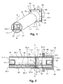
- a tubular housing 10 according to the invention is shown with a therein arranged with a lightning protection circuit arranged therein for a computer network connection on a rectangular printed circuit board 20 in a perspective view.
- a first and front tubular or hollow cylindrical housing part 11 protrudes Fig. 1 obliquely to the rear and is the end face of a second and further behind lying hollow cylindrical housing part 12, so that the two hollow cylindrical housing parts 11, 12 are arranged coaxially with respect to their longitudinal axes.
- a first fastening flange 70 which faces away from the first hollow cylindrical housing part 11, a first fastening flange 70 with a square outer shape protrudes perpendicularly from the second housing part 12.
- the first attachment flange 70 is located approximately in the center thereof with respect to the longitudinal direction of the second hollow-cylindrical housing part 12. In each of the four corner regions of the first attachment flange 70, a respective attachment hole 71 ... 74 is arranged, which completely penetrates the first attachment flange 70.
- the four side lengths of the square first mounting flange 70 measure z. B. each 33 mm.
- the second hollow cylindrical housing part 12 Directly behind the second hollow cylindrical housing part 12 includes a in Fig. 1 non-visible third hollow cylindrical housing part 13, which is aligned with respect to its longitudinal axis ebenfall coaxial with the first and second housing part 11, 12.
- the third housing part 13 has at the first and front end 13.1 (in Fig. 1 not visible, see Fig. 2 ) a directly adjacent to the first mounting flange 70 of the second housing part 12 second mounting flange 80, which protrudes perpendicular to the longitudinal axis of the second housing part 12 of this.
- the second mounting flange 80 has substantially the same dimensions as the first mounting flange 70 and also has four further through holes 81 ... 84 in the corner areas. The four holes 81 ...
- the housing 10 z. B. with screws on a third element Fasten.
- the second housing part 12 facing away from the second end of 13 2 (in Fig. 1 not visible, see Fig. 2 ) of the third hollow cylindrical housing part 13 is in Fig. 1 closed with a cylindrical cap 90.
- first socket 31 for example in the form of a commercially available RJ 45 socket, mounted on the printed circuit board 20.
- the foremost end of the first socket 31 is also flush with the first end 11.2 of the first housing part 11, so that the first socket is laterally completely surrounded by the first housing part 11.
- the three aluminum hollow cylindrical housing parts 11, 12, 13 have, apart from the two mounting flanges 70, 80, essentially an identical outer diameter, which z. B. measures about 28 mm.
- the total length, measured in the direction of the longitudinal axes of the three coaxially arranged housing parts 11, 12, 13 is for example about 112 mm.
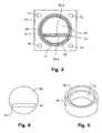
- Fig. 2 is a longitudinal section along the line A - B of the tubular housing 10 from Fig. 1 shown.
- the three hollow cylindrical housing parts 11, 12, 13 are in Fig. 2 with their longitudinal axis arranged horizontally next to each other.
- the second housing part 12 lies to the right of the first housing part 11 and the third housing part 13 is located on the right side in Fig. 2 , directly to the right of the second housing part.
- the first and free end 11.1 of the first housing part 11 points to the left.
- the inner diameter of the first housing part 11 widens in a stepped manner.
- the inner diameter of the second housing part 12 also widens stepwise, specifically in such a way that it corresponds to the widened inner diameter of the first housing part 11 in the region of the second end 11.2.
- a cylindrical connecting ring 50 is pressed with its half width.
- the longitudinal axis of the connecting ring 50 is also aligned coaxially with the longitudinal axes of the first and the second housing part 11, 12.
- the outer diameter of the connecting ring 50 corresponds approximately to the expanded inner diameter of the first housing part 11 in the region of the second end 11.2 and the expanded inner diameter of the second housing part 12 in the region of the first end 12.1.
- the other half of the connecting ring 50 is pressed in the same way in the area with expanded inner diameter of the first end 12.1 of the second housing part 12.
- the minimum inner diameter of the connecting ring 50 region of the narrower ring opening 51 is approximately equal to the minimum inner diameter of the first two housing parts 11, 12.
- the connecting ring consists z. B. copper and connects the two first housing parts non-positively and positively with each other.
- the inner diameter of the second housing part 12 also widens stepwise.
- the outer diameter of the third housing part 13 is tapered stepwise in such a way that it corresponds approximately to the expanded inner diameter in the region of the second end 12.2 of the second housing part 12.
- the first and tapered end 13.1 of the third housing part is present in the region of the second end 12.2 of the second housing part 12 and is pressed with this positive and positive fit.
- the three hollow cylindrical housing parts are therefore mechanically stable connected to each other and together form the robust tubular housing 10th
- the first attachment flange 70 protruding perpendicularly from the second hollow-cylindrical housing part 12 and the second attachment flange 80 protruding perpendicularly from the third hollow-cylindrical housing part 13 directly lie directly against one another on their mutually facing surfaces.
- a cylindrical cap 90 is also arranged, which closes the third housing part 13.
- the Cap 90 is formed as a closed hollow cylinder on one side, which surrounds the third housing part 13 in the region of its second and end 13.2 outside.
- To attach the cap 90 is z. B. a per se known bayonet mechanism provided so that a simple release of the cap 90 by hand is possible.
- the inner diameter of the connecting ring 50 widens from its second (in Fig. 2 right) end face to its first end face (in Fig. 2 left) stepwise, so that there is a narrow ring opening 51 on the right and a wide ring opening 52 on the left (see also Fig. 5 ).
- a circular disc 60 In the wide annular opening 52 of the connecting ring 50 is a circular disc 60, z. B. of copper introduced.
- the outer diameter of the circular disc 60 corresponds approximately to the inner diameter of the connecting ring 50 in the region of the wide annular opening 52.
- the circular disc 60 is located with its right side of the paragraph, which is formed by the step-like transition between wide ring opening 52 and narrow ring opening 51.
- the circular disc 60 lies on the projection, which is formed by the step-like transition of the inner diameter of the first housing part 11.
- the circular disc 60 is held in the wide region 52 of the connecting ring 50.
- the circular disc 60 thus separates the interior of the housing 10 in a first subspace 10.1 and a second subspace 10.2.
- a non-radially extending slot 61 is further introduced (see also Fig. 4 ), which in a direction perpendicular to the sheet in Fig. 2 runs.
- the slot 61 serves to receive the rectangular printed circuit board 20 which extends in a horizontal plane from the first end 11.1 of the first housing part 11 through the second housing part 12 through to the second end 13.2 of the third housing part 13.
- the printed circuit board 20 extends approximately in the middle of the lower half of the housing 10, in a direction parallel to the coaxial longitudinal axes of the three housing parts 11, 12, 13.
- Das in Fig. 2 left front end 20.1 of the printed circuit board 20 is approximately flush with the first end 11.1 of the first housing part 11.
- the printed circuit board 20 is supported in a central region 20.3, which lies between the front end 20.1 and the rear end 20.2 of the printed circuit board 20 through the circular disk 60 and the partition wall in the region of the slot 61.
- the slot 61 is dimensioned such that the circular disk 60 bears against both the upper side 20.5 of the printed circuit board 20 and the underside 20.4 of the printed circuit board 20 and thus mechanically supports the printed circuit board 20 above and below.
- a first socket 31 is disposed directly on the top 20.5 of the printed circuit board 20, wherein it is as in Fig. 1 already mentioned z. B. is a commercially available RJ 45 socket.
- the left-side opening of the socket 31 is approximately flush with the front end 20.1 of the printed circuit board 20 and with the first end 11.1 of the first housing part.
- a second socket 32 also of the type RJ 45, attached to the upper side 20.5 of the printed circuit board 20.
- the opening of the second socket 32 is approximately flush with the rear end 20.2 of the printed circuit board 20 and the second end 13.2 of the third housing part 13.
- the two centers of the openings of the two opposite aligned sockets 31, 32 are located approximately on the coaxial longitudinal central axes of three housing parts 11, 12, 13.
- a plurality of electronic components 40 are arranged on the printed circuit board 20 in the first subspace 10.1 of the housing 10.
- the electronic components have a small height relative to the printed circuit board 20 and are arranged both on the upper side 20.5, as well as on the underside 20.4 of the printed circuit board 20.
- the two subspaces 10.1 and 10.2 of the housing 10 are provided with an in Fig. 2 Gussmasse not shown filled, which completely fills the two subspaces 10.1, 10.2 at least up to the rear ends of the two sockets 31, 32.
- the casting material is present both above and below the printed circuit board 20, so that the printed circuit board 20 is at least partially embedded in the casting compound.
- the electronic components 40, 41 are protected on the printed circuit board 20 from moisture and water. If watertight versions are also used for the two sockets 31, 32, this results in the best possible protection against moisture and water.
- the second socket 32 is also of an in Fig. 2 surrounded by a dashed rectangle only indicated version 32.1 is surrounded.
- the socket 32.1 is used for fixing and centering of the socket 32 in the third housing part 13th
- Fig. 3 is a cross section taken along the line C - D Fig. 2 which runs in a region between the electronic components 40 and the circular disk 60 or the connecting ring 50 perpendicular to the longitudinal central axis through the housing 10.
- the in the central area of Fig. 3 arranged circular disc 60 is concealed in its peripheral edge region of the first non-expanded portion of the first hollow cylindrical housing part 11.
- the rectangular cross-section printed circuit board 20 is arranged in the slot 61.
- the slot 61 has an in Fig. 3 extending in the vertical direction slot width, which corresponds to a thickness of the printed circuit board 20.
- the Fig. 3 in the horizontal direction extending slot length corresponds approximately to the width of the printed circuit board 20.
- the printed circuit board 20 is located with its left side of the in Fig. 3 on the left rear end of the slot 61.1.
- the top 20.5 and the bottom 20.4 of the circuit board is also on the entire width of the printed circuit board 20 at the top and the lower slot limit.
- the printed circuit board is on the top 20.5, the bottom 20.4 and the left side completely against the circular disc 60 and is surrounded by this.
- the circuit board is mechanically fixed in the housing 10 through the circular disc 60 and the partition. In particular, the critical for the printed circuit board 20 bending upward or downward is prevented.
- the slot 61 is completely filled by the printed circuit board 20 or covered by the first housing part 11. Between the first housing part 11 and the in Fig. 3 invisible behind lying second housing part 12 so there is only a small passage opening, so that the two subspaces 10.1, 10.2 of the housing 10 are substantially separated from each other.
- Fig. 4 the circular disc 60 is shown in a plan view.
- the slot 61 jumps from the right side in Figure 4 in the horizontal and non-radial direction in the lower half of the circular disc 60 in this one.
- the slot 61 has an upper and a lower boundary, which run essentially parallel to one another.
- This in Fig. 4 left rear end 61.1 of the slot 61 is perpendicular to the upper or lower boundary of the slot 61. Since the slot 61 is not completely continuous, the circular disc 60 consists of a single piece, which is particularly advantageous during assembly.
- Fig. 5 shows the connecting ring 50 with its longitudinal axis in the vertical direction in detail.
- the connecting ring 50 is substantially formed as a hollow cylinder, which is a in Fig. 5 overhead wide ring opening 52 and a in Fig. 5 below has narrow annular opening 51.
- the wide ring opening 52 goes about halfway up the connecting ring 50 in a stepwise manner into the narrow ring opening 51.
- the rectangular printed circuit board 20 is shown in a plan view on its upper side 20.5.
- the first socket 31 is arranged flush with the front end 20.1.
- the second socket 32 is correspondingly mounted flush with the rear end 20.2.
- the electrical ground contact 20.6 of the printed circuit board is also attached. This is in the form of a rectangular metal strip, which runs with its longer side perpendicular to the longitudinal axis of the rectangular printed circuit board and extends over almost the entire width of the printed circuit board 20. Earth contact 20.6 will be as in Fig. 2 mentioned z. B. soldered to the circular disc 60, so that an electrical contract is formed.
- Fig. 7 shows the three housing parts 11, 12, 13, the connecting ring 50 and the circular disc 60 prior to assembly in a coaxial arrangement.
- the finished assembled printed circuit board 20 is inserted into the slot 61 of the circular disc 60 and then soldered the ground contact 20.6 on the printed circuit board 20 with the circular disc in a first step.
- the circular disc 60 is inserted with inserted circuit board 20 from the side of the wide ring opening 52 forth through the connecting ring 50 until the circular disc 60 abuts the step at the transition to the narrow annular opening 51 of the connecting ring 50.
- one half of the connecting ring 50 is pressed into the region of the second end 11.2 of the first housing part 11 with widened inner diameter until it stops.
- the other half of the connecting ring 50 is in the region of the first end 12.1 of the second housing part 12 with widened Inner diameter also pressed to the stop.
- Disk 60 and connecting ring 50 are soldered together.
- the housing 10 is rotated with its longitudinal axis in the vertical direction and filled from above through the frontal opening of the first end 11.1 of the first housing part 11 casting compound. After a short curing phase, the housing is rotated through 180 °, so that the casting compound can be filled through the opening in the region of the second end 12. 2 of the second housing part 12.
- the pressing in of the first and tapered end 13.1 of the third housing part 13 takes place in the region of the second end 12.2 of the second housing part 12 with widened inner diameter.
- a second housing 100 is shown in a perspective view.
- This one has an in Fig. 8 behind vertical front plate 111, at which in a lower region after a right angle forward projecting forward bottom plate 112 is welded.
- Front plate 111 and bottom plate 112 are made of aluminum.
- From each of the four corner regions of the bottom plate 112 protrudes a retaining pin 161, 162, 163, 164, z. B. in the form of a threaded rod upwards.
- an upper printed circuit board 120 is arranged, wherein the four retaining pins 161 ...
- the upper printed circuit board 120 is z. B. held by not shown nuts in a known manner by the four retaining pins 161 ... 164.
- the threaded rods can at the same time as lightning current arrester, so that no separate lightning conductor must be provided.
- a plane-parallel printed circuit board lower 121 is fixed in the same manner to the four retaining pins 161 ... 164.
- a total of six plug sockets 131... 136 which are of the RJ 45 type, are arranged directly next to one another on the upper side of the upper printed circuit board 120. Accordingly, on the lower printed circuit board 121 at the rear end 121.2 also a total of six other sockets 181 ... 186, also of the type RJ 45, mounted directly on the underside of the lower printed circuit board 121 side by side.
- the openings of all sockets 131 ... 136, 181, 186 protrude in a direction opposite to the front panel 111 direction.
- component portion 140 By a dashed rectangle indicated component portion 140 electronic components are arranged in a known manner. In the present case, it is z.
- electronic components are arranged in a known manner. In the present case, it is z.
- six lightning protection circuits for six computer network connections Analogously, the lower printed circuit board 121 is equipped with, for example, six lightning protection circuits.
- a total of twelve lightning protection circuits for twelve computer network connections are present in the housing 100.
- Fig. 9 is a plan view of the front panel 111 of the housing 100 from Fig. 8 displayed.
- a commercially available fifty-pin connector 150 is inserted, which is electrically connected behind the front panel 111 with the terminals, not shown, on the upper printed circuit board 120 and the lower printed circuit board 121.
- the connector 150 serves to output network signals.
- the total of four holes 171 ... 174 can be seen.
- the housing part 11, 12, 13 in addition to or instead of compression by screwing or cohesive connections (welding, gluing, soldering) to connect with each other.
- z. B. also the third housing part 13 are connected to a further connecting ring with the second housing part 12.
- sockets can be mounted in the region of the lateral surface of the housing, if this is expedient and as sockets other types can be used as the described RJ 45 sockets. Further, it is conceivable to omit the female connector 31 and instead to solder the cable directly to the printed circuit board.
- the circular disc 60 z. B. outside the connecting ring 50 directly in the first housing part 11 or in the second housing part 12 are arranged.
- z. B. a paragraph in one of said housing parts are arranged, which serves as a support for the partition.
- the partition can in principle also be secured by screwing in the housing 10.
Landscapes
- Engineering & Computer Science (AREA)
- Microelectronics & Electronic Packaging (AREA)
- Casings For Electric Apparatus (AREA)
- Shielding Devices Or Components To Electric Or Magnetic Fields (AREA)
Claims (18)
- Dispositif comprenant un circuit imprimé (20, 120, 121) disposé dans un boîtier (10, 100) pour un circuit électrique et/ou électronique, le circuit imprimé (20, 120, 121) présentant une zone avant (20.1, 121.1, 121.1) et une zone arrière (20.2, 120.2, 121.2), le circuit imprimé (20, 120, 121) étant soutenu mécaniquement dans le boîtier (10, 100) entre la zone avant (20.1, 121.1, 121.1) et la zone arrière (20.2, 120.2, 121.2), un espace intérieur du boîtier étant séparé en deux espaces partiels (10.1, 10.2) par une paroi de séparation (60),
caractérisé en ce
que le circuit imprimé (20) fait saillie à travers une fente (61) aménagée dans la paroi de séparation (60) et est soutenu par la paroi de séparation (60). - Dispositif selon la revendication 1, caractérisé en ce que la fente (61) dans la paroi de séparation (60) est dimensionnée de telle sorte que celle-ci est entièrement remplie par une zone (20.3) du circuit imprimé (20) qui est présente dans la fente (61).
- Dispositif selon la revendication 1 ou 2, caractérisé en ce que le circuit imprimé (20) est disposé perpendiculairement à la paroi de séparation (60).
- Dispositif selon l'une des revendications 1 à 3, caractérisé en ce que la paroi de séparation (60) se compose de métal, notamment de cuivre, et est reliée électriquement avec un contact électrique (20.6) introduit dans le circuit imprimé (20), notamment un contact de terre.
- Dispositif selon la revendication 4, caractérisé en ce que le contact électrique (20.6) introduit dans le circuit imprimé (20) est disposé au moins partiellement dans la fente (61) de la paroi de séparation (60) et est fixé par brasage pour établir le contact électrique avec la paroi de séparation (60).
- Dispositif selon l'une des revendications 1 à 5, caractérisé en ce que la paroi de séparation (60) et le boîtier (10) sont reliés électriquement.
- Dispositif selon l'une des revendications 1 à 6, caractérisé en ce que le boîtier (10) est réalisé en forme de tube avec une section transversale circulaire et en ce que la paroi de séparation (60) se présente sous la forme d'une plaque circulaire qui est orientée perpendiculairement à un axe longitudinal du boîtier (10).
- Dispositif selon la revendication 7, caractérisé en ce que le boîtier (10) en forme de tube est réalisé en plusieurs parties, une première partie de boîtier (11) en forme de tube étant reliée du côté frontal avec une deuxième partie de boîtier (12) en forme de tube par le biais d'une bague de liaison (50) intérieure et disposée de manière coaxiale.
- Dispositif selon la revendication 8, caractérisé en ce que la bague de liaison (50) est logée avec une première moitié par adhérence et par complémentarité de forme dans une zone d'extrémité (11.2) ayant un diamètre intérieur agrandi de la première partie de boîtier (11) en forme de tube, alors que la bague de liaison (50) est logée avec une deuxième moitié à la fois par adhérence et par complémentarité de forme dans une deuxième zone d'extrémité (12.1) ayant un diamètre intérieur agrandi de la deuxième partie de boîtier (12) en forme de tube.
- Dispositif selon la revendication 8 ou 9, caractérisé en ce que la plaque circulaire (60) est logée dans la bague de liaison (50), un diamètre de la plaque circulaire (60) correspondant à un diamètre intérieur de la bague de liaison (50) et la plaque circulaire (60) reposant de préférence sur un surplomb faisant saillie vers l'intérieur de la bague de liaison (50).
- Dispositif selon l'une des revendications 7 à 10, caractérisé en ce que la fente (61) présente dans la plaque circulaire (60) s'étend dans une direction non radiale.
- Dispositif selon l'une des revendications 1 à 11, caractérisé en ce que le boîtier (10, 100) se compose de métal, notamment d'aluminium.
- Dispositif selon l'une des revendications 1 à 12, caractérisé en ce qu'un circuit de protection contre la foudre, notamment pour une liaison de réseau informatique, est disposé sur le circuit imprimé (20).
- Dispositif selon l'une des revendications 1 à 13, caractérisé en ce que le circuit imprimé (20) est entouré au moins partiellement par une masse de moulage pour sa protection contre l'humidité et les corps étrangers.
- Dispositif selon l'une des revendications 1 à 14, caractérisé en ce qu'une prise de connexion (31, 32) destinée à la liaison électrique avec un câble externe est présente sur un côté frontal avant et/ou sur un côté frontal arrière du boîtier (10), la prise de connexion (31, 32) étant de préférence montée directement sur le circuit imprimé (20).
- Dispositif selon l'une des revendications 1 à 15, caractérisé en ce que le boîtier (10) dispose sur un côté extérieur d'une ou plusieurs parties en saillie (70, 80) pour la fixation du boîtier (10) à un élément tiers, les parties en saillie (70, 80) présentant notamment des orifices de fixation (71 ... 74, 81 ... 84).
- Dispositif selon l'une des revendications 1 à 16, caractérisé en ce qu'au moins deux circuits imprimés (120, 121) sont disposés avec leurs faces parallèles et espacés l'un au-dessus de l'autre.
- Procédé de fabrication d'un boîtier (10) comprenant un circuit imprimé (20) selon l'une des revendications 7 à 17, caractérisé en ce qu'un circuit imprimé (20) est inséré dans une fente (61) d'une plaque circulaire (60) et la plaque (60) est ensuite logée dans une bague de liaison (50) et la bague de liaison (50) est ensuite coincée avec une première moitié dans une zone d'extrémité (11.2) côté frontal d'une première partie de boîtier (11) en forme de tube et la bague de liaison (50) est ensuite coincée avec une deuxième moitié dans une deuxième zone d'extrémité (12.1) d'une deuxième partie de boîtier (12) en forme de tube.
Applications Claiming Priority (1)
| Application Number | Priority Date | Filing Date | Title |
|---|---|---|---|
| CH3562008A CH706251B1 (de) | 2008-03-11 | 2008-03-11 | Gehäuse mit Leiterplatine. |
Publications (3)
| Publication Number | Publication Date |
|---|---|
| EP2101554A2 EP2101554A2 (fr) | 2009-09-16 |
| EP2101554A3 EP2101554A3 (fr) | 2011-03-16 |
| EP2101554B1 true EP2101554B1 (fr) | 2013-01-02 |
Family
ID=40756336
Family Applications (1)
| Application Number | Title | Priority Date | Filing Date |
|---|---|---|---|
| EP20090405030 Ceased EP2101554B1 (fr) | 2008-03-11 | 2009-02-16 | Boîtier doté d'une platine conductrice |
Country Status (2)
| Country | Link |
|---|---|
| EP (1) | EP2101554B1 (fr) |
| CH (1) | CH706251B1 (fr) |
Families Citing this family (1)
| Publication number | Priority date | Publication date | Assignee | Title |
|---|---|---|---|---|
| DE102009060872A1 (de) † | 2009-12-30 | 2011-08-18 | Baumer Innotec Ag | Sensor mit Gehäuse und Verfahren zu dessen Herstellung |
Family Cites Families (5)
| Publication number | Priority date | Publication date | Assignee | Title |
|---|---|---|---|---|
| US4400858A (en) * | 1981-01-30 | 1983-08-30 | Tele-Drill Inc, | Heat sink/retainer clip for a downhole electronics package of a measurements-while-drilling telemetry system |
| US5034856A (en) * | 1989-10-24 | 1991-07-23 | Hewlett-Packard Company | Modular housing assembly for two incompatible circuits |
| EP0986293A1 (fr) * | 1998-09-08 | 2000-03-15 | Lucent Technologies Inc. | Radio frequency electronic apparatus |
| DE20115670U1 (de) * | 2001-09-24 | 2002-02-21 | TRW Automotive Electronics & Components GmbH & Co. KG, 78315 Radolfzell | Gehäuse für ein elektronisches Steuergerät in Fahrzeugen |
| US7048564B1 (en) * | 2005-05-27 | 2006-05-23 | Delphi Technologies, Inc. | Sealed electronic module with fastenerless circuit board support post |
-
2008
- 2008-03-11 CH CH3562008A patent/CH706251B1/de not_active IP Right Cessation
-
2009
- 2009-02-16 EP EP20090405030 patent/EP2101554B1/fr not_active Ceased
Also Published As
| Publication number | Publication date |
|---|---|
| EP2101554A2 (fr) | 2009-09-16 |
| EP2101554A3 (fr) | 2011-03-16 |
| CH706251B1 (de) | 2013-09-30 |
Similar Documents
| Publication | Publication Date | Title |
|---|---|---|
| DE3790062C2 (fr) | ||
| EP0921609A2 (fr) | Connecteur coaxial à haute fréquence et à angle droit | |
| EP3164911B1 (fr) | Fiche de raccordement | |
| DE2845234A1 (de) | Kontaktvorrichtung fuer mehrlagenschaltungen | |
| EP4014287B1 (fr) | Connecteur femelle de carte de circuit imprimé xlr à 8+2 voies | |
| EP3435482B1 (fr) | Liaison de connexion comprenant un système de câble et un système de plaque, procédé de fabrication d'une telle liaison de connexion | |
| DE3710394C2 (fr) | ||
| DE202005017012U1 (de) | Elektrische Anschlusseinrichtung für eine Leiterplatte | |
| DE69813640T2 (de) | Elektrische verbinder | |
| DE60008719T2 (de) | Eingangs/ausgangssteckverbinderanordnung mit erdungsanordnung für abgeschirmte kabel und verfahren zur herstellung und zum zusammenbau eines solchen steckverbinders | |
| DE3313967A1 (de) | Vorrichtung zum sicheren herstellen von elektrisch leitenden verbindungen zwischen gehaeuseteilen eines gehaeuses | |
| DE102007039064A1 (de) | Elektronisches Gerät und Leiterplatte mit Steckerleiste | |
| DE202012002352U1 (de) | Anordnung aus Steckverbinder und Leiterplatte | |
| DE7429478U (de) | Steckverbinder für elektronische Geräte | |
| DE19720678C1 (de) | HF-Koaxial-Steckverbinderteil | |
| AT505732A2 (de) | Netzspannungsversorgungsgerät | |
| EP0918374B1 (fr) | Connecteur coaxial à haute fréquence | |
| DE102012005812A1 (de) | Elektrischer Verbinder mit integriertem Impedanzangleichelement | |
| EP0606294A1 (fr) | Construction d'un appareil electrotechnique | |
| EP2101554A2 (fr) | Boîtier doté d'une platine conductrice | |
| AT505742B1 (de) | Elektronisches gerät | |
| DE202009018077U1 (de) | Leistungselektronikanordnung | |
| EP0649192A2 (fr) | Dispositif d'installation électrique avec module supplémentaire | |
| DE3802642C1 (en) | Electrical plug distributor | |
| DE102014012739A1 (de) | Elektrischer Steckverbinder, Verbinderelement und Verwendung |
Legal Events
| Date | Code | Title | Description |
|---|---|---|---|
| PUAI | Public reference made under article 153(3) epc to a published international application that has entered the european phase |
Free format text: ORIGINAL CODE: 0009012 |
|
| AK | Designated contracting states |
Kind code of ref document: A2 Designated state(s): AT BE BG CH CY CZ DE DK EE ES FI FR GB GR HR HU IE IS IT LI LT LU LV MC MK MT NL NO PL PT RO SE SI SK TR |
|
| AX | Request for extension of the european patent |
Extension state: AL BA RS |
|
| PUAL | Search report despatched |
Free format text: ORIGINAL CODE: 0009013 |
|
| AK | Designated contracting states |
Kind code of ref document: A3 Designated state(s): AT BE BG CH CY CZ DE DK EE ES FI FR GB GR HR HU IE IS IT LI LT LU LV MC MK MT NL NO PL PT RO SE SI SK TR |
|
| AX | Request for extension of the european patent |
Extension state: AL BA RS |
|
| 17P | Request for examination filed |
Effective date: 20110830 |
|
| AKX | Designation fees paid |
Designated state(s): CH DE LI |
|
| GRAP | Despatch of communication of intention to grant a patent |
Free format text: ORIGINAL CODE: EPIDOSNIGR1 |
|
| GRAS | Grant fee paid |
Free format text: ORIGINAL CODE: EPIDOSNIGR3 |
|
| GRAA | (expected) grant |
Free format text: ORIGINAL CODE: 0009210 |
|
| AK | Designated contracting states |
Kind code of ref document: B1 Designated state(s): DE |
|
| RBV | Designated contracting states (corrected) |
Designated state(s): DE |
|
| REG | Reference to a national code |
Ref country code: DE Ref legal event code: R096 Ref document number: 502009005872 Country of ref document: DE Effective date: 20130307 |
|
| PLBE | No opposition filed within time limit |
Free format text: ORIGINAL CODE: 0009261 |
|
| STAA | Information on the status of an ep patent application or granted ep patent |
Free format text: STATUS: NO OPPOSITION FILED WITHIN TIME LIMIT |
|
| 26N | No opposition filed |
Effective date: 20131003 |
|
| REG | Reference to a national code |
Ref country code: DE Ref legal event code: R097 Ref document number: 502009005872 Country of ref document: DE Effective date: 20131003 |
|
| PGFP | Annual fee paid to national office [announced via postgrant information from national office to epo] |
Ref country code: DE Payment date: 20190219 Year of fee payment: 11 |
|
| REG | Reference to a national code |
Ref country code: DE Ref legal event code: R119 Ref document number: 502009005872 Country of ref document: DE |
|
| PG25 | Lapsed in a contracting state [announced via postgrant information from national office to epo] |
Ref country code: DE Free format text: LAPSE BECAUSE OF NON-PAYMENT OF DUE FEES Effective date: 20200901 |