EP4014287B1 - Connecteur femelle de carte de circuit imprimé xlr à 8+2 voies - Google Patents
Connecteur femelle de carte de circuit imprimé xlr à 8+2 voies Download PDFInfo
- Publication number
- EP4014287B1 EP4014287B1 EP20758118.2A EP20758118A EP4014287B1 EP 4014287 B1 EP4014287 B1 EP 4014287B1 EP 20758118 A EP20758118 A EP 20758118A EP 4014287 B1 EP4014287 B1 EP 4014287B1
- Authority
- EP
- European Patent Office
- Prior art keywords
- housing
- contacts
- connector according
- sections
- chassis connector
- Prior art date
- Legal status (The legal status is an assumption and is not a legal conclusion. Google has not performed a legal analysis and makes no representation as to the accuracy of the status listed.)
- Active
Links
Images


Classifications
-
- H—ELECTRICITY
- H01—ELECTRIC ELEMENTS
- H01R—ELECTRICALLY-CONDUCTIVE CONNECTIONS; STRUCTURAL ASSOCIATIONS OF A PLURALITY OF MUTUALLY-INSULATED ELECTRICAL CONNECTING ELEMENTS; COUPLING DEVICES; CURRENT COLLECTORS
- H01R24/00—Two-part coupling devices, or either of their cooperating parts, characterised by their overall structure
- H01R24/38—Two-part coupling devices, or either of their cooperating parts, characterised by their overall structure having concentrically or coaxially arranged contacts
- H01R24/40—Two-part coupling devices, or either of their cooperating parts, characterised by their overall structure having concentrically or coaxially arranged contacts specially adapted for high frequency
- H01R24/50—Two-part coupling devices, or either of their cooperating parts, characterised by their overall structure having concentrically or coaxially arranged contacts specially adapted for high frequency mounted on a PCB [Printed Circuit Board]
-
- H—ELECTRICITY
- H01—ELECTRIC ELEMENTS
- H01R—ELECTRICALLY-CONDUCTIVE CONNECTIONS; STRUCTURAL ASSOCIATIONS OF A PLURALITY OF MUTUALLY-INSULATED ELECTRICAL CONNECTING ELEMENTS; COUPLING DEVICES; CURRENT COLLECTORS
- H01R12/00—Structural associations of a plurality of mutually-insulated electrical connecting elements, specially adapted for printed circuits, e.g. printed circuit boards [PCB], flat or ribbon cables, or like generally planar structures, e.g. terminal strips, terminal blocks; Coupling devices specially adapted for printed circuits, flat or ribbon cables, or like generally planar structures; Terminals specially adapted for contact with, or insertion into, printed circuits, flat or ribbon cables, or like generally planar structures
- H01R12/70—Coupling devices
- H01R12/71—Coupling devices for rigid printing circuits or like structures
- H01R12/72—Coupling devices for rigid printing circuits or like structures coupling with the edge of the rigid printed circuits or like structures
- H01R12/722—Coupling devices for rigid printing circuits or like structures coupling with the edge of the rigid printed circuits or like structures coupling devices mounted on the edge of the printed circuits
- H01R12/724—Coupling devices for rigid printing circuits or like structures coupling with the edge of the rigid printed circuits or like structures coupling devices mounted on the edge of the printed circuits containing contact members forming a right angle
-
- H—ELECTRICITY
- H01—ELECTRIC ELEMENTS
- H01R—ELECTRICALLY-CONDUCTIVE CONNECTIONS; STRUCTURAL ASSOCIATIONS OF A PLURALITY OF MUTUALLY-INSULATED ELECTRICAL CONNECTING ELEMENTS; COUPLING DEVICES; CURRENT COLLECTORS
- H01R13/00—Details of coupling devices of the kinds covered by groups H01R12/70 or H01R24/00 - H01R33/00
- H01R13/02—Contact members
-
- H—ELECTRICITY
- H01—ELECTRIC ELEMENTS
- H01R—ELECTRICALLY-CONDUCTIVE CONNECTIONS; STRUCTURAL ASSOCIATIONS OF A PLURALITY OF MUTUALLY-INSULATED ELECTRICAL CONNECTING ELEMENTS; COUPLING DEVICES; CURRENT COLLECTORS
- H01R13/00—Details of coupling devices of the kinds covered by groups H01R12/70 or H01R24/00 - H01R33/00
- H01R13/40—Securing contact members in or to a base or case; Insulating of contact members
- H01R13/42—Securing in a demountable manner
- H01R13/436—Securing a plurality of contact members by one locking piece or operation
- H01R13/4367—Insertion of locking piece from the rear
-
- H—ELECTRICITY
- H01—ELECTRIC ELEMENTS
- H01R—ELECTRICALLY-CONDUCTIVE CONNECTIONS; STRUCTURAL ASSOCIATIONS OF A PLURALITY OF MUTUALLY-INSULATED ELECTRICAL CONNECTING ELEMENTS; COUPLING DEVICES; CURRENT COLLECTORS
- H01R13/00—Details of coupling devices of the kinds covered by groups H01R12/70 or H01R24/00 - H01R33/00
- H01R13/46—Bases; Cases
- H01R13/502—Bases; Cases composed of different pieces
-
- H—ELECTRICITY
- H01—ELECTRIC ELEMENTS
- H01R—ELECTRICALLY-CONDUCTIVE CONNECTIONS; STRUCTURAL ASSOCIATIONS OF A PLURALITY OF MUTUALLY-INSULATED ELECTRICAL CONNECTING ELEMENTS; COUPLING DEVICES; CURRENT COLLECTORS
- H01R24/00—Two-part coupling devices, or either of their cooperating parts, characterised by their overall structure
- H01R24/86—Parallel contacts arranged about a common axis
-
- H—ELECTRICITY
- H01—ELECTRIC ELEMENTS
- H01R—ELECTRICALLY-CONDUCTIVE CONNECTIONS; STRUCTURAL ASSOCIATIONS OF A PLURALITY OF MUTUALLY-INSULATED ELECTRICAL CONNECTING ELEMENTS; COUPLING DEVICES; CURRENT COLLECTORS
- H01R27/00—Coupling parts adapted for co-operation with two or more dissimilar counterparts
- H01R27/02—Coupling parts adapted for co-operation with two or more dissimilar counterparts for simultaneous co-operation with two or more dissimilar counterparts
-
- H—ELECTRICITY
- H01—ELECTRIC ELEMENTS
- H01R—ELECTRICALLY-CONDUCTIVE CONNECTIONS; STRUCTURAL ASSOCIATIONS OF A PLURALITY OF MUTUALLY-INSULATED ELECTRICAL CONNECTING ELEMENTS; COUPLING DEVICES; CURRENT COLLECTORS
- H01R2107/00—Four or more poles
Definitions
- the invention relates to an electrical built-in connector, in particular for connecting to electronic circuit boards.
- Such built-in connectors also known as built-in sockets or chassis sockets
- XLR versions for installation in control panels, control cabinets or the walls of device housings and are designed for connection to standard circuit boards used in the entertainment industry. They are available in a wide variety of designs, i.e. with different numbers and designs of contacts, as well as with different grounding and connection variants and as male and female plugs.
- Three- to five-pin built-in sockets are also known in designs for connecting to horizontal circuit boards.
- the electrical contacts of these designs are guided outwards at one end of the housing parallel to the longitudinal axis of the housing and then run at an angle, with the connection areas to the circuit board ending in a common plane, which plane is parallel to the longitudinal axis of the housing.
- the connection areas can also be on the outside of a plate-shaped element. If more data or energy channels are required, these built-in sockets can no longer be used.
- XLR connectors of type 8 + 2 which offer two power channels in addition to eight data channels. Due to the large number of contacts protruding from the rear face, the connection to a circuit board has so far only been possible in a vertical arrangement, where the circuit board is oriented parallel to the rear face and thus perpendicular to the longitudinal axis of the housing. This means that a connection to horizontal circuit boards is not possible, which limits the application area of these connectors.
- the JP 2015 115546 A a "surface-mounted device” component whose circuit board is permanently provided with a connector housing mounted on its surface.
- Contact pins protrude freely into the interior of this housing, i.e. the receiving area for a complementary connector, and are guided outwards on the rear side parallel to the axis.
- a deflection takes place on the rear side of the housing by 90° towards the circuit board, where a solder connection is made between the free running ends of the contact pins and the connection contacts on the circuit board.
- the ends of the contact pins are arranged in an arrangement of three parallel straight lines.
- the US 2011/053427 A1 is an electrical connector that is also designed for mounting on a circuit arrangement.
- Contact pins are held in two insulating contact carriers arranged one behind the other and are bent by 90° within this contact carrier arrangement. The ends of the contact pins emerge from the contact carrier arrangement in a bent manner and are then arranged in a number of parallel straight lines.
- the contact carrier arrangement itself is inserted into a metal housing from the rear and protrudes beyond this housing at the rear.
- the EP0561202A1 discloses earth connections with integral tail shielding.
- Their connector arrangement is designed for mounting on a circuit arrangement and comprises an insulating housing and an arrangement of contact elements held directly in this housing. These are arranged in a plurality of rows and columns in the housing.
- the contact elements are oriented parallel to one another and to the insertion direction and in this arrangement also emerge from the housing on the rear side, ie opposite the insertion side. Outside the housing, each contact element has a curve or a bent section which then continues in a straight line to the circuit arrangement, where contact is also made in an arrangement with several rows and columns.
- an electrical built-in connector with a housing, with at least one mounting structure projecting transversely to the longitudinal axis of the housing, and with an inserted contact carrier made of electrically insulating material.
- the contacts are guided outwards at one end of the housing parallel to the longitudinal axis, the end sections of the sections lying outside the housing being angled compared to their sections lying inside the housing and their connection areas intended for connection to a circuit board ending in a common plane, which plane lies parallel to the longitudinal axis of the housing. This plane is preferably located radially further outside than a tangential plane parallel to it on the housing.
- connection areas of the contact elements are arranged in groups on at least three parallel straight lines that are part of the common plane.
- the ends of the sections of the contacts that lead out of the housing in parallel are at the same distance in the direction of the longitudinal axis of the housing as the parallel straight lines. This results in a staggered position of the deflection points from parallel to angled direction along the longitudinal axis of the housing, which provides sufficient space for the contact-free arrangement and a sufficiently spaced-apart course of the angled sections of the contacts.
- the task underlying the invention was an easy-to-use connector with a large number of data or energy channels, which is also suitable for connection to a horizontally positioned circuit board.
- the contact carrier is fixed in the housing on the side of the housing on which the contacts are guided on the outside thereof, by means of a ring which projects inwards from the housing wall at least in places and is connected to the housing wall at least at one point.
- eight contacts are provided for data transmission and two contacts for energy transmission in order to meet a standard design.
- the contacts for energy transmission have a larger diameter than the contacts for data transmission. This means that higher currents can be transmitted to ensure sufficient energy supply, while smaller conductor cross-sections are sufficient for data transmission using low voltages and currents, and a higher number of these can be provided per socket.
- a secure connection between the retaining element and the housing can be established quickly and easily if the retaining element and the housing wall are crimped together at least at one point.
- a preferred embodiment of a built-in connector as a male plug provides that the electrical contacts are designed as contact pins.
- the electrical contacts are designed as at least ring-shaped contact openings.
- a mounting structure is provided according to a first embodiment, which is at least one laterally projecting ear with a mounting hole.
- a mounting hole is provided that is opposite one another with respect to the central axis of the housing.
- the mounting structure is a flange that projects over the entire circumference of the housing and in which at least one mounting hole is machined.
- at least two mounting holes are arranged in the flange, opposite one another in relation to the center axis of the housing. This can have a rectangular shape or can also have a circular or elliptical shape.
- the angled sections of the contacts run straight and parallel to one another over a large part of their length. This results in the necessary mutual spacing of the electrically conductive elements with a simple design.
- the angled sections are separate elements - i.e. they are not manufactured in one piece with the contacts housed in the housing and led out through the contact carrier - and are directly connected to the sections of the contacts that lead to the outside of the housing. This can be done by screwing, riveting or welding and, if necessary, gluing with conductive adhesives.
- the angled sections are fixed in a common holding plate shortly before their connection areas.
- This holding plate is preferably also located radially outside a parallel tangential plane to the housing.
- the common retaining plate can also have an extension running along the housing to ensure a firm fit and good connection to the circuit board, but also to connect the retaining plate to the housing better and in a mechanically secure manner.
- interlocking guide or stabilizing arrangements can also be arranged in or on the housing and the extension of the retaining plate.
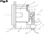
- the electrical built-in connector shown as an example in the attached drawings in a version as an 8 + 2 built-in socket with the option of connecting to an electronic circuit board has a housing 1.
- This can be made of a plastic or a metallic material.
- a rectangular or square mounting flange 2 is provided as a mounting structure projecting transversely to the longitudinal axis A of the housing 1.
- Mounting holes 3 are machined into the corners of this mounting flange 2 opposite the longitudinal center axis A in order to be able to attach the built-in plug socket to a control panel, a device wall or the like using mounting screws, rivets or similar fastening means extending through these mounting holes 3.
- the mounting flange 2 could also be circular, elliptical, with any polygonal peripheral edge or in a similar manner.
- mounting ears with holes protruding laterally from a cylindrically shaped housing 1 are also possible, with two ears opposite each other in relation to the longitudinal axis A of the housing 1 being preferred.
- the housing 1 surrounds a total of 10 contact pins 4, 5 as a male connector. These are in a contact carrier 6 (see Fig. 3 and Fig. 4 ) which is manufactured separately from the housing 1 and is inserted therein parallel to the longitudinal axis A of the housing 1.
- the contact carrier 6 consists of an electrically insulating material, in particular plastic, and leaves the end sections pointing towards the complementary connector exposed.
- the contact carrier 4 which then extends all the way to the front end of the housing 1, accommodates ring-shaped or hollow-cylindrical contact elements.
- contacts 4 are intended for energy transmission and eight contacts 5 are intended for data transmission.
- the contacts 4 for energy transmission are preferably designed with a larger diameter than the thinner contacts 5 for data transmission.
- the contact elements here the contact pins 4, 5, run parallel to the longitudinal axis A of the housing 1 and are guided outwards on the rear side of the contact carrier 6 at one end or of the housing 1 or through both components 1, 4, also parallel to the longitudinal axis A of the housing 1 and protrude from the front side of the housing 1 opposite the insertion side for the cable plug.
- the end sections 41, 51 of the sections of the contacts 4, 5 located outside the housing 1 are angled compared to their sections located inside the housing 1. These end sections 41, 51 typically run transversely to the longitudinal axis A of the housing 1 and, at least from a certain distance from the contacts 4, 5, also parallel to one another. At their outermost ends, they merge into connection areas 42, 52 provided for connection to an electronic circuit board. These end in a common plane E, which parallel to the longitudinal axis A of the housing 1, and preferably also outside of its enveloping surface.
- the connecting areas 42, 52 are arranged in groups, whereby the individual groups - as in the Fig.4 and Fig.5 can be clearly seen - lie on at least three parallel lines G (see Fig.4 ), which are part of the common plane E. In Fig.5 these straight lines G would pass perpendicular to the plane of the drawing through the connecting regions 42, 52.
- the end sections 41, 51 can be designed as a direct continuation of the contacts 4, 5 and can be made by folding or bending from a direction parallel to the longitudinal axis A into a direction transverse to it and parallel to one another.
- an embodiment as shown in the drawing figures is preferred, in which the angled sections 41, 51 are produced as separate elements which are then directly connected to the sections of the contacts 4, 5 that lead to the outside of the housing, for example by riveting, as can be seen in the drawings.
- the end sections 41, 51 are preferably designed as flat metal strips, with the connecting sections 42, 52 preferably having a smaller width than the majority of the length of the end sections 41, 51.
- the angled sections 41, 51 of the contacts 4, 5 are fixed shortly before their connection areas 42, 52 in a common holding plate 9, from which the connection areas 42, 52 protrude on the side facing the circuit board in order to be able to be connected to this circuit board.
- the common holding plate 9 is preferably provided with an extension 91 running along the housing 1, which, together with the holding plate 9, provides a firm support and good connection to the circuit board and also ensures the mechanically stable connection between the housing 1 and the precisely defined position of the connection areas 42, 52.
- the ends of the sections of the contacts 4, 5 that extend parallel to one another and to the longitudinal axis A from the housing 1 have the same distance in the direction of the longitudinal axis A of the housing 1 as the parallel straight lines G or vice versa.
- the contact carrier 6, which is preferably inserted into the housing 1, is fixed in the housing 1 by means of a ring 7 on the side of the housing 1 on which the contacts 4, 5 are guided on the outside.
- the ring 7 is at least partially designed to project inwards from the rear end face of the wall of the housing 1, overlapping the rear end face of the contact carrier 6 and thus preventing the latter from being pushed out of the housing 1 to the rear.
- the ring 7 is firmly connected to the housing 1 at least at one point. This connection can be made by crimping a tongue 71 of the ring 7, which extends radially outwards between two pins 8 of the housing 1, to these pins 8.
- the front insertion opening in the housing 1 preferably has a cutout 21 at at least one circumferential position, which continues parallel to the longitudinal axis A of the housing 1 to the rear into the interior of the housing.
- the contact carrier 6 can also have a recess 61 at a corresponding position. This cutout 21 and the recess 61 serve as a receptacle for a locking mechanism 10 of known design, which in Fig.2 is shown schematically.
Landscapes
- Coupling Device And Connection With Printed Circuit (AREA)
- Connector Housings Or Holding Contact Members (AREA)
- Details Of Connecting Devices For Male And Female Coupling (AREA)
- Multi-Conductor Connections (AREA)
Claims (12)
- Connecteur électrique encastrable, avec un boîtier (1), avec au moins une structure de montage (2) en saillie transversalement à l'axe longitudinal du boîtier, avec un support de contacts (6) en matériau électriquement isolant qui est inséré dans le boîtier (1) parallèlement à l'axe longitudinal (A) de celui-ci, avec plus de cinq contacts électriques (4, 5) fixés dans le support de contacts (6), les contacts (4, 5) étant guidés à une extrémité du boîtier (1) en dehors du support de contacts (6) et du boîtier (1) vers l'extérieur parallèlement à l'axe longitudinal (A) du boîtier (1), les parties d'extrémité (41, 51) des parties des contacts (4, 5) situées à l'extérieur du boîtier (1) étant coudées par rapport à leurs parties situées à l'intérieur du boîtier (1), et des zones de connexion (42, 52) prévues pour leur connexion avec une platine se terminant dans un plan commun (E), lequel plan (E) est parallèle à l'axe longitudinal (A) du boîtier (1), les zones de connexion (42, 52) étant disposées en groupes et les groupes individuels étant situés sur au moins trois droites parallèles (G) qui font partie du plan commun (E), les extrémités des parties des contacts (4, 5) guidées en dehors du boîtier (1) parallèlement à l'axe longitudinal (A) du boîtier (1) présentant le même écartement que les droites parallèles (G), caractérisé en ce que le support de contacts (6) est fixé dans le boîtier, sur le côté du boîtier (1) sur lequel les contacts (4, 5) sont guidés vers l'extérieur de celui-ci, au moyen d'une bague (7) qui fait saillie vers l'intérieur, au moins par endroits, de la paroi de boîtier et qui est reliée à la paroi de boîtier en au moins un endroit.
- Connecteur encastrable selon la revendication 1, dans lequel huit contacts (5) sont prévus pour la transmission de données et deux contacts (4) pour la transmission d'énergie.
- Connecteur encastrable selon la revendication 2, dans lequel les contacts (4) pour la transmission d'énergie présentent un diamètre plus grand que les contacts (5) pour la transmission de données.
- Connecteur encastrable selon la revendication 1, dans lequel l'élément de retenue (7) et la paroi de boîtier sont sertis ensemble en au moins un endroit.
- Connecteur encastrable selon la revendication 1, dans lequel les contacts électriques (4, 5) sont réalisés sous la forme de broches de contact.
- Connecteur encastrable selon la revendication 1, dans lequel les contacts électriques (4, 5) sont réalisés sous la forme d'ouvertures de contact au moins annulaires.
- Connecteur encastrable selon la revendication 1, dans lequel la structure de montage (2) est au moins une oreille en saillie latérale avec un perçage de montage (3).
- Connecteur encastrable selon la revendication 1, dans lequel la structure de montage (2) est une bride en saillie sur toute la périphérie du boîtier (1), dans laquelle est réalisé au moins un perçage de montage (3).
- Connecteur encastré selon la revendication 1, dans lequel les parties coudées (41, 51) sont droites et parallèles entre elles sur une grande partie de leur longueur.
- Connecteur encastrable selon la revendication 1, dans lequel les parties coudées (41, 51) sont des éléments séparés et sont directement reliées aux parties des contacts (4, 5) qui sont guidées vers l'extérieur du boîtier (1).
- Connecteur encastrable selon la revendication 1, dans lequel les parties coudées (41, 51) sont fixées dans une plaque de retenue commune (9) juste avant leurs zones de connexion (42, 52).
- Connecteur encastrable selon la revendication 11, dans lequel la plaque de retenue commune (9) présente un prolongement s'étendant le long du boîtier (1) en contact avec celui-ci.
Applications Claiming Priority (2)
| Application Number | Priority Date | Filing Date | Title |
|---|---|---|---|
| CN201921311838.7U CN210137029U (zh) | 2019-08-13 | 2019-08-13 | 嵌入式插接连接器 |
| PCT/EP2020/025371 WO2021028077A1 (fr) | 2019-08-13 | 2020-08-12 | Connecteur femelle de carte de circuit imprimé xlr à 8+2 voies |
Publications (2)
| Publication Number | Publication Date |
|---|---|
| EP4014287A1 EP4014287A1 (fr) | 2022-06-22 |
| EP4014287B1 true EP4014287B1 (fr) | 2024-05-29 |
Family
ID=69708175
Family Applications (1)
| Application Number | Title | Priority Date | Filing Date |
|---|---|---|---|
| EP20758118.2A Active EP4014287B1 (fr) | 2019-08-13 | 2020-08-12 | Connecteur femelle de carte de circuit imprimé xlr à 8+2 voies |
Country Status (10)
| Country | Link |
|---|---|
| US (1) | US11881662B2 (fr) |
| EP (1) | EP4014287B1 (fr) |
| JP (1) | JP7334332B2 (fr) |
| KR (1) | KR20220020996A (fr) |
| CN (2) | CN210137029U (fr) |
| AU (1) | AU2020328093A1 (fr) |
| BR (1) | BR112022001686A2 (fr) |
| CA (1) | CA3148768A1 (fr) |
| MX (1) | MX2022001572A (fr) |
| WO (1) | WO2021028077A1 (fr) |
Families Citing this family (4)
| Publication number | Priority date | Publication date | Assignee | Title |
|---|---|---|---|---|
| CN210137029U (zh) * | 2019-08-13 | 2020-03-10 | 纽陲客股份公司 | 嵌入式插接连接器 |
| DE102021118853B4 (de) * | 2021-07-21 | 2023-06-15 | Amphenol Tuchel Industrial GmbH | Mehrteiliger Leiterplattenadapterstecker mit spezifischem Interface |
| DE102023000370A1 (de) * | 2022-02-22 | 2023-08-24 | Neutrik Ag | Steckverbinder-Anordnung für elektrische Steckverbinder |
| KR20240013570A (ko) * | 2022-07-22 | 2024-01-30 | 삼성전자주식회사 | 관통 홀이 형성된 하우징을 포함하는 전자 장치 |
Citations (3)
| Publication number | Priority date | Publication date | Assignee | Title |
|---|---|---|---|---|
| US4921431A (en) * | 1989-01-23 | 1990-05-01 | Switchcraft, Inc. | Connector adapter assembly |
| EP0561202A1 (fr) * | 1992-03-20 | 1993-09-22 | Connector Systems Technology N.V. | Borne de terre intégrale et blindage pour extrémité de connexion |
| US5975917A (en) * | 1998-04-01 | 1999-11-02 | Hon Hai Precision Ind. Co., Ltd. | Method for manufacturing an electrical connector and electrical connector manufactured by the same |
Family Cites Families (24)
| Publication number | Priority date | Publication date | Assignee | Title |
|---|---|---|---|---|
| JPH0822182B2 (ja) | 1989-09-04 | 1996-03-06 | 株式会社クボタ | コンバインのクラッチ操作構造 |
| JP2581782Y2 (ja) * | 1991-10-14 | 1998-09-24 | 日本航空電子工業株式会社 | 多芯l型同軸コネクタ |
| US5752854A (en) * | 1997-02-18 | 1998-05-19 | The Whitaker Corporation | Panel mount structure |
| JP4201782B2 (ja) | 2004-06-03 | 2008-12-24 | タイコエレクトロニクスアンプ株式会社 | 基板実装型電気コネクタ |
| CN201230018Y (zh) * | 2008-05-29 | 2009-04-29 | 富士康(昆山)电脑接插件有限公司 | 电连接器 |
| TWM376943U (en) * | 2009-09-03 | 2010-03-21 | Hon Hai Prec Ind Co Ltd | Electrical connector |
| US8292662B2 (en) * | 2010-09-19 | 2012-10-23 | Cheng Uei Precision Industry Co., Ltd. | Watertight connector |
| US9590339B2 (en) * | 2013-05-09 | 2017-03-07 | Commscope, Inc. Of North Carolina | High data rate connectors and cable assemblies that are suitable for harsh environments and related methods and systems |
| JP6130244B2 (ja) * | 2013-06-27 | 2017-05-17 | 矢崎総業株式会社 | 端子及び充電コネクタ |
| JP6362857B2 (ja) | 2013-12-13 | 2018-07-25 | 株式会社東海理化電機製作所 | 実装品及びその製造方法 |
| JP6246650B2 (ja) * | 2014-04-11 | 2017-12-13 | タイコエレクトロニクスジャパン合同会社 | 表面実装コネクタ |
| DE102014111831A1 (de) * | 2014-08-19 | 2016-02-25 | Phoenix Contact E-Mobility Gmbh | Steckverbinderteil mit Temperatursensoren |
| DE102016105470A1 (de) * | 2016-03-23 | 2017-09-28 | Te Connectivity Germany Gmbh | Leistungselektrische Kontakteinrichtung; austauschbares, leistungselektrisches Kontaktmodul sowie leistungselektrischer Verbinder |
| DE102016211876A1 (de) * | 2016-06-30 | 2018-01-04 | Phoenix Contact E-Mobility Gmbh | Elektroanschlusseinrichtung mit verbesserter thermischer Kopplung einer einen Temperatursensor aufweisenden Platine |
| CN207052813U (zh) | 2017-05-12 | 2018-02-27 | 泰科电子(上海)有限公司 | 插座壳体组件及插座 |
| JP6656206B2 (ja) * | 2017-05-26 | 2020-03-04 | 矢崎総業株式会社 | コネクタ |
| JP2019016531A (ja) * | 2017-07-07 | 2019-01-31 | 株式会社オートネットワーク技術研究所 | 基板用コネクタ及び回路基板と基板用コネクタの接続構造 |
| TWI806883B (zh) * | 2017-07-31 | 2023-07-01 | 美商康寧光纖通信射頻有限責任公司 | 雙軸的電纜連接器和雙軸的電纜組件 |
| JP6933304B2 (ja) * | 2018-07-20 | 2021-09-08 | 株式会社オートネットワーク技術研究所 | コネクタ及び外導体 |
| JP6996445B2 (ja) * | 2018-07-20 | 2022-01-17 | 株式会社オートネットワーク技術研究所 | シールドコネクタ及び外導体端子 |
| CN210137029U (zh) * | 2019-08-13 | 2020-03-10 | 纽陲客股份公司 | 嵌入式插接连接器 |
| KR102733088B1 (ko) * | 2019-09-11 | 2024-11-20 | 주식회사 엘지에너지솔루션 | 보호소자 통합형 커넥터 |
| KR102843254B1 (ko) * | 2020-05-04 | 2025-08-05 | 주식회사 엘지에너지솔루션 | 커넥터 모듈 |
| JP7414635B2 (ja) * | 2020-05-07 | 2024-01-16 | 日本航空電子工業株式会社 | コネクタ組立体 |
-
2019
- 2019-08-13 CN CN201921311838.7U patent/CN210137029U/zh active Active
-
2020
- 2020-08-12 BR BR112022001686A patent/BR112022001686A2/pt not_active Application Discontinuation
- 2020-08-12 MX MX2022001572A patent/MX2022001572A/es unknown
- 2020-08-12 CA CA3148768A patent/CA3148768A1/fr not_active Abandoned
- 2020-08-12 AU AU2020328093A patent/AU2020328093A1/en not_active Abandoned
- 2020-08-12 EP EP20758118.2A patent/EP4014287B1/fr active Active
- 2020-08-12 KR KR1020227003141A patent/KR20220020996A/ko active Pending
- 2020-08-12 WO PCT/EP2020/025371 patent/WO2021028077A1/fr not_active Ceased
- 2020-08-12 JP JP2022508796A patent/JP7334332B2/ja active Active
- 2020-08-12 US US17/629,221 patent/US11881662B2/en active Active
- 2020-08-12 CN CN202080056649.9A patent/CN114375527A/zh not_active Withdrawn
Patent Citations (3)
| Publication number | Priority date | Publication date | Assignee | Title |
|---|---|---|---|---|
| US4921431A (en) * | 1989-01-23 | 1990-05-01 | Switchcraft, Inc. | Connector adapter assembly |
| EP0561202A1 (fr) * | 1992-03-20 | 1993-09-22 | Connector Systems Technology N.V. | Borne de terre intégrale et blindage pour extrémité de connexion |
| US5975917A (en) * | 1998-04-01 | 1999-11-02 | Hon Hai Precision Ind. Co., Ltd. | Method for manufacturing an electrical connector and electrical connector manufactured by the same |
Also Published As
| Publication number | Publication date |
|---|---|
| JP2022544653A (ja) | 2022-10-20 |
| CN210137029U (zh) | 2020-03-10 |
| BR112022001686A2 (pt) | 2022-03-22 |
| MX2022001572A (es) | 2022-03-02 |
| CN114375527A (zh) | 2022-04-19 |
| US11881662B2 (en) | 2024-01-23 |
| AU2020328093A1 (en) | 2022-03-24 |
| EP4014287A1 (fr) | 2022-06-22 |
| CA3148768A1 (fr) | 2021-01-08 |
| JP7334332B2 (ja) | 2023-08-28 |
| WO2021028077A1 (fr) | 2021-02-18 |
| KR20220020996A (ko) | 2022-02-21 |
| US20220320807A1 (en) | 2022-10-06 |
Similar Documents
| Publication | Publication Date | Title |
|---|---|---|
| EP4014287B1 (fr) | Connecteur femelle de carte de circuit imprimé xlr à 8+2 voies | |
| DE69120688T2 (de) | Mehrpoliger abgeschirmter verbinder mit gemeinsamer erdung | |
| EP3031103B1 (fr) | Système comprenant une pluralité de modules de connecteur électrique et un cadre de support électriquement conducteur | |
| EP2603952B1 (fr) | Connecteur enfichable pour transmission des données différentielle | |
| AT523135B1 (de) | Kontaktträger für elektrische Steckverbinder und Steckverbinder hierfür | |
| EP3164911B1 (fr) | Fiche de raccordement | |
| EP0921609A2 (fr) | Connecteur coaxial à haute fréquence et à angle droit | |
| EP3353859B1 (fr) | Dispositif de connexion pour conducteur | |
| EP0247662A1 (fr) | Connexion de traversée pour signaux HF | |
| EP3017510B1 (fr) | Connecteur à fiche | |
| DE2845234A1 (de) | Kontaktvorrichtung fuer mehrlagenschaltungen | |
| DE202012007216U1 (de) | Kontaktelement | |
| EP4235976B1 (fr) | Connecteur enfichable comprenant un pont conducteur de protection | |
| EP0205876A1 (fr) | Dispositif multipolaire enfichable comportant une réglette de positionnement avec un dispositif de blindage | |
| WO2015032516A1 (fr) | Dispositif à traversée murale | |
| EP3170230A1 (fr) | Système de sortie de boîtier modulaire | |
| DE3308492C2 (de) | Mehrpolige Steckverbindung | |
| DE102007039064A1 (de) | Elektronisches Gerät und Leiterplatte mit Steckerleiste | |
| DE202012002352U1 (de) | Anordnung aus Steckverbinder und Leiterplatte | |
| EP3963674B1 (fr) | Interface pour carte de circuit imprimé | |
| EP2200125B1 (fr) | Connecteur à fiches blindé | |
| DE19720678C1 (de) | HF-Koaxial-Steckverbinderteil | |
| DE69117257T2 (de) | Stecker und Buchse eines Mikrostreifen-Leitung-Verbinders | |
| EP2034568B1 (fr) | Boîte de raccordement pour technologie des données | |
| DE19640847B4 (de) | Rechtwinkliger abgeschirmter elektrischer Verbinder |
Legal Events
| Date | Code | Title | Description |
|---|---|---|---|
| STAA | Information on the status of an ep patent application or granted ep patent |
Free format text: STATUS: UNKNOWN |
|
| STAA | Information on the status of an ep patent application or granted ep patent |
Free format text: STATUS: THE INTERNATIONAL PUBLICATION HAS BEEN MADE |
|
| PUAI | Public reference made under article 153(3) epc to a published international application that has entered the european phase |
Free format text: ORIGINAL CODE: 0009012 |
|
| STAA | Information on the status of an ep patent application or granted ep patent |
Free format text: STATUS: REQUEST FOR EXAMINATION WAS MADE |
|
| 17P | Request for examination filed |
Effective date: 20220307 |
|
| AK | Designated contracting states |
Kind code of ref document: A1 Designated state(s): AL AT BE BG CH CY CZ DE DK EE ES FI FR GB GR HR HU IE IS IT LI LT LU LV MC MK MT NL NO PL PT RO RS SE SI SK SM TR |
|
| DAV | Request for validation of the european patent (deleted) | ||
| DAX | Request for extension of the european patent (deleted) | ||
| REG | Reference to a national code |
Ref country code: DE Ref legal event code: R079 Free format text: PREVIOUS MAIN CLASS: H01R0024500000 Ipc: H01R0012720000 Ref document number: 502020008162 Country of ref document: DE |
|
| GRAP | Despatch of communication of intention to grant a patent |
Free format text: ORIGINAL CODE: EPIDOSNIGR1 |
|
| STAA | Information on the status of an ep patent application or granted ep patent |
Free format text: STATUS: GRANT OF PATENT IS INTENDED |
|
| RIC1 | Information provided on ipc code assigned before grant |
Ipc: H01R 107/00 20060101ALN20240112BHEP Ipc: H01R 13/436 20060101ALN20240112BHEP Ipc: H01R 24/86 20110101ALI20240112BHEP Ipc: H01R 12/72 20110101AFI20240112BHEP |
|
| INTG | Intention to grant announced |
Effective date: 20240201 |
|
| GRAS | Grant fee paid |
Free format text: ORIGINAL CODE: EPIDOSNIGR3 |
|
| GRAA | (expected) grant |
Free format text: ORIGINAL CODE: 0009210 |
|
| STAA | Information on the status of an ep patent application or granted ep patent |
Free format text: STATUS: THE PATENT HAS BEEN GRANTED |
|
| AK | Designated contracting states |
Kind code of ref document: B1 Designated state(s): AL AT BE BG CH CY CZ DE DK EE ES FI FR GB GR HR HU IE IS IT LI LT LU LV MC MK MT NL NO PL PT RO RS SE SI SK SM TR |
|
| REG | Reference to a national code |
Ref country code: CH Ref legal event code: EP |
|
| REG | Reference to a national code |
Ref country code: IE Ref legal event code: FG4D Free format text: LANGUAGE OF EP DOCUMENT: GERMAN |
|
| REG | Reference to a national code |
Ref country code: DE Ref legal event code: R096 Ref document number: 502020008162 Country of ref document: DE |
|
| REG | Reference to a national code |
Ref country code: LT Ref legal event code: MG9D |
|
| REG | Reference to a national code |
Ref country code: NL Ref legal event code: MP Effective date: 20240529 |
|
| PG25 | Lapsed in a contracting state [announced via postgrant information from national office to epo] |
Ref country code: IS Free format text: LAPSE BECAUSE OF FAILURE TO SUBMIT A TRANSLATION OF THE DESCRIPTION OR TO PAY THE FEE WITHIN THE PRESCRIBED TIME-LIMIT Effective date: 20240929 |
|
| PG25 | Lapsed in a contracting state [announced via postgrant information from national office to epo] |
Ref country code: BG Free format text: LAPSE BECAUSE OF FAILURE TO SUBMIT A TRANSLATION OF THE DESCRIPTION OR TO PAY THE FEE WITHIN THE PRESCRIBED TIME-LIMIT Effective date: 20240529 |
|
| PG25 | Lapsed in a contracting state [announced via postgrant information from national office to epo] |
Ref country code: FI Free format text: LAPSE BECAUSE OF FAILURE TO SUBMIT A TRANSLATION OF THE DESCRIPTION OR TO PAY THE FEE WITHIN THE PRESCRIBED TIME-LIMIT Effective date: 20240529 Ref country code: HR Free format text: LAPSE BECAUSE OF FAILURE TO SUBMIT A TRANSLATION OF THE DESCRIPTION OR TO PAY THE FEE WITHIN THE PRESCRIBED TIME-LIMIT Effective date: 20240529 |
|
| PG25 | Lapsed in a contracting state [announced via postgrant information from national office to epo] |
Ref country code: GR Free format text: LAPSE BECAUSE OF FAILURE TO SUBMIT A TRANSLATION OF THE DESCRIPTION OR TO PAY THE FEE WITHIN THE PRESCRIBED TIME-LIMIT Effective date: 20240830 |
|
| PG25 | Lapsed in a contracting state [announced via postgrant information from national office to epo] |
Ref country code: ES Free format text: LAPSE BECAUSE OF FAILURE TO SUBMIT A TRANSLATION OF THE DESCRIPTION OR TO PAY THE FEE WITHIN THE PRESCRIBED TIME-LIMIT Effective date: 20240529 |
|
| PG25 | Lapsed in a contracting state [announced via postgrant information from national office to epo] |
Ref country code: PL Free format text: LAPSE BECAUSE OF FAILURE TO SUBMIT A TRANSLATION OF THE DESCRIPTION OR TO PAY THE FEE WITHIN THE PRESCRIBED TIME-LIMIT Effective date: 20240529 |
|
| PG25 | Lapsed in a contracting state [announced via postgrant information from national office to epo] |
Ref country code: LV Free format text: LAPSE BECAUSE OF FAILURE TO SUBMIT A TRANSLATION OF THE DESCRIPTION OR TO PAY THE FEE WITHIN THE PRESCRIBED TIME-LIMIT Effective date: 20240529 |
|
| PG25 | Lapsed in a contracting state [announced via postgrant information from national office to epo] |
Ref country code: PL Free format text: LAPSE BECAUSE OF FAILURE TO SUBMIT A TRANSLATION OF THE DESCRIPTION OR TO PAY THE FEE WITHIN THE PRESCRIBED TIME-LIMIT Effective date: 20240529 Ref country code: NO Free format text: LAPSE BECAUSE OF FAILURE TO SUBMIT A TRANSLATION OF THE DESCRIPTION OR TO PAY THE FEE WITHIN THE PRESCRIBED TIME-LIMIT Effective date: 20240829 Ref country code: LV Free format text: LAPSE BECAUSE OF FAILURE TO SUBMIT A TRANSLATION OF THE DESCRIPTION OR TO PAY THE FEE WITHIN THE PRESCRIBED TIME-LIMIT Effective date: 20240529 Ref country code: IS Free format text: LAPSE BECAUSE OF FAILURE TO SUBMIT A TRANSLATION OF THE DESCRIPTION OR TO PAY THE FEE WITHIN THE PRESCRIBED TIME-LIMIT Effective date: 20240929 Ref country code: HR Free format text: LAPSE BECAUSE OF FAILURE TO SUBMIT A TRANSLATION OF THE DESCRIPTION OR TO PAY THE FEE WITHIN THE PRESCRIBED TIME-LIMIT Effective date: 20240529 Ref country code: GR Free format text: LAPSE BECAUSE OF FAILURE TO SUBMIT A TRANSLATION OF THE DESCRIPTION OR TO PAY THE FEE WITHIN THE PRESCRIBED TIME-LIMIT Effective date: 20240830 Ref country code: FI Free format text: LAPSE BECAUSE OF FAILURE TO SUBMIT A TRANSLATION OF THE DESCRIPTION OR TO PAY THE FEE WITHIN THE PRESCRIBED TIME-LIMIT Effective date: 20240529 Ref country code: ES Free format text: LAPSE BECAUSE OF FAILURE TO SUBMIT A TRANSLATION OF THE DESCRIPTION OR TO PAY THE FEE WITHIN THE PRESCRIBED TIME-LIMIT Effective date: 20240529 Ref country code: BG Free format text: LAPSE BECAUSE OF FAILURE TO SUBMIT A TRANSLATION OF THE DESCRIPTION OR TO PAY THE FEE WITHIN THE PRESCRIBED TIME-LIMIT Effective date: 20240529 Ref country code: RS Free format text: LAPSE BECAUSE OF FAILURE TO SUBMIT A TRANSLATION OF THE DESCRIPTION OR TO PAY THE FEE WITHIN THE PRESCRIBED TIME-LIMIT Effective date: 20240829 |
|
| PG25 | Lapsed in a contracting state [announced via postgrant information from national office to epo] |
Ref country code: NL Free format text: LAPSE BECAUSE OF FAILURE TO SUBMIT A TRANSLATION OF THE DESCRIPTION OR TO PAY THE FEE WITHIN THE PRESCRIBED TIME-LIMIT Effective date: 20240529 |
|
| PG25 | Lapsed in a contracting state [announced via postgrant information from national office to epo] |
Ref country code: NL Free format text: LAPSE BECAUSE OF FAILURE TO SUBMIT A TRANSLATION OF THE DESCRIPTION OR TO PAY THE FEE WITHIN THE PRESCRIBED TIME-LIMIT Effective date: 20240529 |
|
| PG25 | Lapsed in a contracting state [announced via postgrant information from national office to epo] |
Ref country code: DK Free format text: LAPSE BECAUSE OF FAILURE TO SUBMIT A TRANSLATION OF THE DESCRIPTION OR TO PAY THE FEE WITHIN THE PRESCRIBED TIME-LIMIT Effective date: 20240529 |
|
| PG25 | Lapsed in a contracting state [announced via postgrant information from national office to epo] |
Ref country code: EE Free format text: LAPSE BECAUSE OF FAILURE TO SUBMIT A TRANSLATION OF THE DESCRIPTION OR TO PAY THE FEE WITHIN THE PRESCRIBED TIME-LIMIT Effective date: 20240529 |
|
| PG25 | Lapsed in a contracting state [announced via postgrant information from national office to epo] |
Ref country code: CZ Free format text: LAPSE BECAUSE OF FAILURE TO SUBMIT A TRANSLATION OF THE DESCRIPTION OR TO PAY THE FEE WITHIN THE PRESCRIBED TIME-LIMIT Effective date: 20240529 |
|
| PG25 | Lapsed in a contracting state [announced via postgrant information from national office to epo] |
Ref country code: RO Free format text: LAPSE BECAUSE OF FAILURE TO SUBMIT A TRANSLATION OF THE DESCRIPTION OR TO PAY THE FEE WITHIN THE PRESCRIBED TIME-LIMIT Effective date: 20240529 Ref country code: SK Free format text: LAPSE BECAUSE OF FAILURE TO SUBMIT A TRANSLATION OF THE DESCRIPTION OR TO PAY THE FEE WITHIN THE PRESCRIBED TIME-LIMIT Effective date: 20240529 |
|
| PG25 | Lapsed in a contracting state [announced via postgrant information from national office to epo] |
Ref country code: SM Free format text: LAPSE BECAUSE OF FAILURE TO SUBMIT A TRANSLATION OF THE DESCRIPTION OR TO PAY THE FEE WITHIN THE PRESCRIBED TIME-LIMIT Effective date: 20240529 |
|
| PG25 | Lapsed in a contracting state [announced via postgrant information from national office to epo] |
Ref country code: SM Free format text: LAPSE BECAUSE OF FAILURE TO SUBMIT A TRANSLATION OF THE DESCRIPTION OR TO PAY THE FEE WITHIN THE PRESCRIBED TIME-LIMIT Effective date: 20240529 Ref country code: SK Free format text: LAPSE BECAUSE OF FAILURE TO SUBMIT A TRANSLATION OF THE DESCRIPTION OR TO PAY THE FEE WITHIN THE PRESCRIBED TIME-LIMIT Effective date: 20240529 Ref country code: RO Free format text: LAPSE BECAUSE OF FAILURE TO SUBMIT A TRANSLATION OF THE DESCRIPTION OR TO PAY THE FEE WITHIN THE PRESCRIBED TIME-LIMIT Effective date: 20240529 Ref country code: EE Free format text: LAPSE BECAUSE OF FAILURE TO SUBMIT A TRANSLATION OF THE DESCRIPTION OR TO PAY THE FEE WITHIN THE PRESCRIBED TIME-LIMIT Effective date: 20240529 Ref country code: DK Free format text: LAPSE BECAUSE OF FAILURE TO SUBMIT A TRANSLATION OF THE DESCRIPTION OR TO PAY THE FEE WITHIN THE PRESCRIBED TIME-LIMIT Effective date: 20240529 Ref country code: CZ Free format text: LAPSE BECAUSE OF FAILURE TO SUBMIT A TRANSLATION OF THE DESCRIPTION OR TO PAY THE FEE WITHIN THE PRESCRIBED TIME-LIMIT Effective date: 20240529 |
|
| PG25 | Lapsed in a contracting state [announced via postgrant information from national office to epo] |
Ref country code: IT Free format text: LAPSE BECAUSE OF FAILURE TO SUBMIT A TRANSLATION OF THE DESCRIPTION OR TO PAY THE FEE WITHIN THE PRESCRIBED TIME-LIMIT Effective date: 20240529 |
|
| REG | Reference to a national code |
Ref country code: DE Ref legal event code: R097 Ref document number: 502020008162 Country of ref document: DE |
|
| REG | Reference to a national code |
Ref country code: CH Ref legal event code: PL |
|
| PLBE | No opposition filed within time limit |
Free format text: ORIGINAL CODE: 0009261 |
|
| STAA | Information on the status of an ep patent application or granted ep patent |
Free format text: STATUS: NO OPPOSITION FILED WITHIN TIME LIMIT |
|
| PG25 | Lapsed in a contracting state [announced via postgrant information from national office to epo] |
Ref country code: LU Free format text: LAPSE BECAUSE OF NON-PAYMENT OF DUE FEES Effective date: 20240812 |
|
| GBPC | Gb: european patent ceased through non-payment of renewal fee |
Effective date: 20240829 |
|
| PG25 | Lapsed in a contracting state [announced via postgrant information from national office to epo] |
Ref country code: CH Free format text: LAPSE BECAUSE OF NON-PAYMENT OF DUE FEES Effective date: 20240831 Ref country code: SI Free format text: LAPSE BECAUSE OF FAILURE TO SUBMIT A TRANSLATION OF THE DESCRIPTION OR TO PAY THE FEE WITHIN THE PRESCRIBED TIME-LIMIT Effective date: 20240529 Ref country code: MC Free format text: LAPSE BECAUSE OF FAILURE TO SUBMIT A TRANSLATION OF THE DESCRIPTION OR TO PAY THE FEE WITHIN THE PRESCRIBED TIME-LIMIT Effective date: 20240529 |
|
| 26N | No opposition filed |
Effective date: 20250303 |
|
| REG | Reference to a national code |
Ref country code: BE Ref legal event code: MM Effective date: 20240831 |
|
| PG25 | Lapsed in a contracting state [announced via postgrant information from national office to epo] |
Ref country code: GB Free format text: LAPSE BECAUSE OF NON-PAYMENT OF DUE FEES Effective date: 20240829 |
|
| PG25 | Lapsed in a contracting state [announced via postgrant information from national office to epo] |
Ref country code: BE Free format text: LAPSE BECAUSE OF NON-PAYMENT OF DUE FEES Effective date: 20240831 |
|
| PG25 | Lapsed in a contracting state [announced via postgrant information from national office to epo] |
Ref country code: FR Free format text: LAPSE BECAUSE OF NON-PAYMENT OF DUE FEES Effective date: 20240831 |
|
| PG25 | Lapsed in a contracting state [announced via postgrant information from national office to epo] |
Ref country code: IE Free format text: LAPSE BECAUSE OF NON-PAYMENT OF DUE FEES Effective date: 20240812 |
|
| PG25 | Lapsed in a contracting state [announced via postgrant information from national office to epo] |
Ref country code: SE Free format text: LAPSE BECAUSE OF FAILURE TO SUBMIT A TRANSLATION OF THE DESCRIPTION OR TO PAY THE FEE WITHIN THE PRESCRIBED TIME-LIMIT Effective date: 20240529 |
|
| PGFP | Annual fee paid to national office [announced via postgrant information from national office to epo] |
Ref country code: DE Payment date: 20250820 Year of fee payment: 6 |
|
| PGFP | Annual fee paid to national office [announced via postgrant information from national office to epo] |
Ref country code: AT Payment date: 20251020 Year of fee payment: 5 |
|
| PG25 | Lapsed in a contracting state [announced via postgrant information from national office to epo] |
Ref country code: PT Free format text: LAPSE BECAUSE OF NON-PAYMENT OF DUE FEES Effective date: 20240529 |
|
| PG25 | Lapsed in a contracting state [announced via postgrant information from national office to epo] |
Ref country code: CY Free format text: LAPSE BECAUSE OF FAILURE TO SUBMIT A TRANSLATION OF THE DESCRIPTION OR TO PAY THE FEE WITHIN THE PRESCRIBED TIME-LIMIT; INVALID AB INITIO Effective date: 20200812 |
|
| PG25 | Lapsed in a contracting state [announced via postgrant information from national office to epo] |
Ref country code: HU Free format text: LAPSE BECAUSE OF FAILURE TO SUBMIT A TRANSLATION OF THE DESCRIPTION OR TO PAY THE FEE WITHIN THE PRESCRIBED TIME-LIMIT; INVALID AB INITIO Effective date: 20200812 |