EP2105522A2 - Installation de cristallisation - Google Patents
Installation de cristallisation Download PDFInfo
- Publication number
- EP2105522A2 EP2105522A2 EP09008527A EP09008527A EP2105522A2 EP 2105522 A2 EP2105522 A2 EP 2105522A2 EP 09008527 A EP09008527 A EP 09008527A EP 09008527 A EP09008527 A EP 09008527A EP 2105522 A2 EP2105522 A2 EP 2105522A2
- Authority
- EP
- European Patent Office
- Prior art keywords
- crystal growing
- coils
- coil
- hollow cylindrical
- cylindrical body
- Prior art date
- Legal status (The legal status is an assumption and is not a legal conclusion. Google has not performed a legal analysis and makes no representation as to the accuracy of the status listed.)
- Withdrawn
Links
Images


Classifications
-
- C—CHEMISTRY; METALLURGY
- C30—CRYSTAL GROWTH
- C30B—SINGLE-CRYSTAL GROWTH; UNIDIRECTIONAL SOLIDIFICATION OF EUTECTIC MATERIAL OR UNIDIRECTIONAL DEMIXING OF EUTECTOID MATERIAL; REFINING BY ZONE-MELTING OF MATERIAL; PRODUCTION OF A HOMOGENEOUS POLYCRYSTALLINE MATERIAL WITH DEFINED STRUCTURE; SINGLE CRYSTALS OR HOMOGENEOUS POLYCRYSTALLINE MATERIAL WITH DEFINED STRUCTURE; AFTER-TREATMENT OF SINGLE CRYSTALS OR A HOMOGENEOUS POLYCRYSTALLINE MATERIAL WITH DEFINED STRUCTURE; APPARATUS THEREFOR
- C30B15/00—Single-crystal growth by pulling from a melt, e.g. Czochralski method
- C30B15/30—Mechanisms for rotating or moving either the melt or the crystal
-
- H—ELECTRICITY
- H10—SEMICONDUCTOR DEVICES; ELECTRIC SOLID-STATE DEVICES NOT OTHERWISE PROVIDED FOR
- H10P—GENERIC PROCESSES OR APPARATUS FOR THE MANUFACTURE OR TREATMENT OF DEVICES COVERED BY CLASS H10
- H10P14/00—Formation of materials, e.g. in the shape of layers or pillars
- H10P14/20—Formation of materials, e.g. in the shape of layers or pillars of semiconductor materials
-
- C—CHEMISTRY; METALLURGY
- C30—CRYSTAL GROWTH
- C30B—SINGLE-CRYSTAL GROWTH; UNIDIRECTIONAL SOLIDIFICATION OF EUTECTIC MATERIAL OR UNIDIRECTIONAL DEMIXING OF EUTECTOID MATERIAL; REFINING BY ZONE-MELTING OF MATERIAL; PRODUCTION OF A HOMOGENEOUS POLYCRYSTALLINE MATERIAL WITH DEFINED STRUCTURE; SINGLE CRYSTALS OR HOMOGENEOUS POLYCRYSTALLINE MATERIAL WITH DEFINED STRUCTURE; AFTER-TREATMENT OF SINGLE CRYSTALS OR A HOMOGENEOUS POLYCRYSTALLINE MATERIAL WITH DEFINED STRUCTURE; APPARATUS THEREFOR
- C30B11/00—Single-crystal growth by normal freezing or freezing under temperature gradient, e.g. Bridgman-Stockbarger method
-
- C—CHEMISTRY; METALLURGY
- C30—CRYSTAL GROWTH
- C30B—SINGLE-CRYSTAL GROWTH; UNIDIRECTIONAL SOLIDIFICATION OF EUTECTIC MATERIAL OR UNIDIRECTIONAL DEMIXING OF EUTECTOID MATERIAL; REFINING BY ZONE-MELTING OF MATERIAL; PRODUCTION OF A HOMOGENEOUS POLYCRYSTALLINE MATERIAL WITH DEFINED STRUCTURE; SINGLE CRYSTALS OR HOMOGENEOUS POLYCRYSTALLINE MATERIAL WITH DEFINED STRUCTURE; AFTER-TREATMENT OF SINGLE CRYSTALS OR A HOMOGENEOUS POLYCRYSTALLINE MATERIAL WITH DEFINED STRUCTURE; APPARATUS THEREFOR
- C30B15/00—Single-crystal growth by pulling from a melt, e.g. Czochralski method
- C30B15/14—Heating of the melt or the crystallised materials
-
- Y—GENERAL TAGGING OF NEW TECHNOLOGICAL DEVELOPMENTS; GENERAL TAGGING OF CROSS-SECTIONAL TECHNOLOGIES SPANNING OVER SEVERAL SECTIONS OF THE IPC; TECHNICAL SUBJECTS COVERED BY FORMER USPC CROSS-REFERENCE ART COLLECTIONS [XRACs] AND DIGESTS
- Y10—TECHNICAL SUBJECTS COVERED BY FORMER USPC
- Y10S—TECHNICAL SUBJECTS COVERED BY FORMER USPC CROSS-REFERENCE ART COLLECTIONS [XRACs] AND DIGESTS
- Y10S117/00—Single-crystal, oriented-crystal, and epitaxy growth processes; non-coating apparatus therefor
- Y10S117/90—Apparatus characterized by composition or treatment thereof, e.g. surface finish, surface coating
-
- Y—GENERAL TAGGING OF NEW TECHNOLOGICAL DEVELOPMENTS; GENERAL TAGGING OF CROSS-SECTIONAL TECHNOLOGIES SPANNING OVER SEVERAL SECTIONS OF THE IPC; TECHNICAL SUBJECTS COVERED BY FORMER USPC CROSS-REFERENCE ART COLLECTIONS [XRACs] AND DIGESTS
- Y10—TECHNICAL SUBJECTS COVERED BY FORMER USPC
- Y10T—TECHNICAL SUBJECTS COVERED BY FORMER US CLASSIFICATION
- Y10T117/00—Single-crystal, oriented-crystal, and epitaxy growth processes; non-coating apparatus therefor
- Y10T117/10—Apparatus
Definitions
- the invention relates to a crystal growing plant, in particular semiconductor crystal growing plant, comprising a heatable crucible for a melt and a coaxial with the crucible arranged coil arrangement for generating a magnetic field in the melt, wherein the coil assembly comprises three or more coils, which are arranged one above the other in the axial direction are and which are each acted upon by an alternating voltage, wherein the voltage applied to a coil AC voltage is phase-shifted with respect to the voltage applied to the adjacent coil AC voltage.
- the systems that work according to the Vertical Gradient Freeze (VGF) method differ from those that operate according to the Czochralski method (CZ) in their construction.
- VGF Vertical Gradient Freeze
- CZ Czochralski method
- the VGF process operates under high overpressure, so the boiler must be made of steel to withstand the high pressure.
- the steel boiler would at least largely shield a magnetic field generated by a coil disposed outside the boiler, so that inside the crucible made of boron nitride or quartz glass is, no sufficiently strong magnetic traveling field would arise to mix the melt. That is, the coil should be placed inside the vessel as close as possible to the crucible, but outside the crucible.
- the coil would at least partially cool the heating power of the heater. Inside the crucible, the coil can not be arranged, as they cause chemical reactions with the melt or, because of the high temperature of the melt itself melt or - if cooled - would prevent the melting of the silicon.
- the invention is therefore based on the problem of providing, by simple means, a magnetic field configuration which is suitable for controlling convections within the melt to such an extent that the crystal drawn from the melt is as homogeneous as possible, thereby heating the melt.
- the invention provides a crystal growing apparatus according to the preamble of claim 1, wherein the coils are formed by a hollow cylindrical body made of an electrically conductive material, which forms by a multi-circumferential slot a single-layer, spiral-shaped current path through connectable to the power supply contact points is divided into sections, each forming a coil.
- the inventive concept is therefore to use a high temperature resistant coil, which does not have to be cooled.
- the next step in the invention is to combine the required heater with the desired coil, by forming the coil from solid graphite conductor rods, which generates the correct magnetic field with adapted resistance and gives off the desired heat output.
- a crucible is used e.g. operated from quartz glass in a vacuum vessel at reduced pressure and inert gas.
- Heaters made of graphite, which are built around the crucible, are known here.
- the busbars are arranged in a meandering manner in a manner which results when a full graphite cylinder is alternately slotted in from top to bottom and from bottom to top and in each case leaves a web for the transverse connection.
- the idea of the invention in the CZ method is now to reshape the already known graphite heater so that the busbars are guided spirally around the crucible, so that the current direction is always the same.
- the inventive coil arrangement for the CZ method acts on the melt like a linear motor, the direction of movement of the outer zones of the melt being directed upwards or downwards depending on the direction of the current.
- the skin effect can be exploited, so that with increasing frequency of the three-phase current, an increasingly thinner zone is moved in the melt.
- a traveling magnetic field can be generated, which penetrates into the region of the semiconductor melt and thereby causes certain flows of the electrically conductive melt which are favorable for the crystal growth process.
- the melt must also be kept at a temperature that is usually slightly above the melting point of the respective material to be melted.
- resistance heaters are arranged around the crucible.
- the coils can additionally take on the heating function: The current flowing through the coil generates heat due to their electrical resistances, which serves both to melt the material in the crucible and to maintain the melting temperature.
- the solution according to the invention has the particular advantage that the hollow cylindrical body forms a particularly good, because evenly radiating heat radiation source because of its largely closed to thin slits inner surface.
- the coils are electrically connected in the form of a star or delta connection with each other, wherein the coils are connected according to their circuitry to the poles of a three-phase power source.
- a three-phase power source are usually available at the installation sites for crystal growth devices, so that a power supply according to the invention for the coils is provided without additional effort.
- the coils are additionally connected to a DC voltage source, which in addition to the AC direct current generated in the coils, which alone is responsible for the heating power.
- the hollow cylindrical body can be provided in a particularly simple manner with a spiral-shaped slot if it passes through the hollow cylindrical body in always the same sense of direction.
- the coils can be supplied with power, have the formation of three coils in the axial direction superposed sections each have two contact points for connection to the phases of a three-phase power source.
- the contact points are connected to extending on the inner or outer circumferential surface of the hollow cylindrical body electrically conductive rails which terminate at an end face of the hollow cylindrical body in terminals which are connected to the phases of a three-phase power source.
- the rails can also act as a resistance heating element of a resistance heater and are connected to a DC voltage source.
- a device for electrical resistance heating of a semiconductor crystal growing system is produced while simultaneously generating a traveling magnetic field.
- the invention thus provides an arrangement of electrical resistance heating elements in a system for Growth of monocrystalline semiconductor crystals from the melt, which are designed so that the alternating current flowing for heating in the resistance heating elements simultaneously generates a magnetic traveling field.
- the invention thus consists essentially of a device for electrical resistance heating a semiconductor crystal growing system, which is determined by the fact that the substantially hollow cylindrical resistance heater consists of three axially superimposed sections, in each case by a substantially spiral slot of the current path a single-layer coil is defined and have the same sense of rotation of the spiral slot, and that the three sections have two contact points for connection to the three phases of a three-phase power source.
- the dual use of the coils as a resistance heater and as a magnetic field generator has the further advantage that they like the previous resistance heaters, which are used exclusively for heating the melt, can be arranged directly on the crucible within a boiler. This is in contrast to the previously known arrangements in which the field coils for magnetic field generation are arranged separately from the resistance heater outside the boiler.
- the invention thus solves the problem by the use of an electrical resistance heater surrounding the melt in the form of a hollow cylindrical body having an array of slots which forces the heating current to a substantially helical path so that the resistance heater simultaneously acts as a single-layer coil acts to generate a magnetic field.
- a material for the resistance heater graphite can be used particularly advantageously, whereby in a protective gas atmosphere, a temperature resistance up to 2000 ° C is achieved.
- the use of cylindrical resistance heating elements of isostatically pressed graphite is today the technical standard in the semiconductor crystal growing industry. When operating the resistance heater with alternating current creates a time-dependent alternating field.
- the invention presented here thus achieves the advantage that the current required for electrical heating of the system is used simultaneously to generate a magnetic field wander.
- the resistance heater which is also designed as a coil arrangement, high temperature resistant and immediately surrounds the hot core zone of the system and thus the melting range. This will change the volume within which the Magnetic field must be generated minimized.
- the alternating magnetic field does not have to penetrate the boiler wall of the crystal growing system, whereby the boiler wall can be carried out in a conventional manner as a steel boiler. As a result, there are no shielding problems for the area outside the plant.
- the generation of magnetic traveling fields in the region of the melt is made possible by the invention in the first place.
- Another significant advantage of the invention presented here is that the hollow cylindrical geometry of the heater coil arrangement already corresponds to the most widely used heater arrangement of crystal growing systems and thus can be combined with existing facilities or even retrofitted without great design effort, if sufficient Number of power feedthroughs is available.
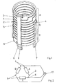
- Fig. 1 an example of a heater-coil arrangement according to the invention is shown, in which a hollow cylindrical body 1, which can be produced particularly advantageously from isostatically pressed graphite, is provided with a substantially spiral-shaped slot 2.
- the term "spiraling" also includes a gradual course, as he in the Fig. 1 is shown.
- the arrangement has four electrical contact points 3, 4, 5 and 6, which serve the supply of alternating currents.
- a delta connection is realized in that the first phase of a three-phase current source by means of a first extending over the height of the hollow cylindrical body 1 rail 8 to the first and fourth contact points connected thereto 3, 6, the second phase by means of a second rail 7 to the second contact point 4 and the third phase is connected by means of a third rail 9 to the third contact point 5.
- the rails 7, 8, 9 can by means of high temperature resistant screws, the z. B. can be made of the carbon fiber material CFC, are bolted to the hollow cylindrical body 1.
- the rails 7, 8, 9 can be screwed with three current feedthroughs in the bottom of a crystal growing system, to which the corresponding high-current cables are connected outside the system.
- a spiral-forming, a rung forming path is formed, which is divided by the contact points 3 to 6 in three sections, each forming a coil A, B, C.
- the tracks are higher than wide and thus on average substantially rectangular.
- the Fig. 2 shows the casing of the three coils A, B, C to a delta connection, wherein the respective adjacent ends of the (cyclic) adjacent coils are connected and are connected to the phases of a three-phase power source.
- the resistance heater presented in this invention consists of three sections stacked in the axial direction, each defined by a pair of taps and thus corresponding to three coaxial coils arranged one above the other.
- the taps can be made by connecting the contact points 3 and 6, 4 and 4, 5 and 5 - as in Fig. 1 and Fig. 2 shown - can be configured as a delta connection and connected to the three phases of a three-phase source.
- the three sections at points 4 and 5 can be separated from each other and then configured as a star connection and connected to the three phases of a three-phase source 17. In both cases, three alternating currents 120 ° out of phase flow through the three sections, generating a traveling magnetic field inside the device.
- This traveling field generates an upward or downward flow in the edge area of a semiconductor melt positioned inside the resistance heater, depending on the sense of circulation of the connection of the three phases with the three sections.
- This can, for. B. in the case of a Czochralski arrangement, the thermal Auftriebskonvetation be counteracted, while in the case of a VGF arrangement by mixing the melt, the effective heat transport can be increased.
- Fig. 3 is the use of a heater-coil assembly according to the invention, namely the hollow cylindrical body 1 as described above, in a high-pressure crystal growing plant for the growth of compound semiconductor crystals shown by the VGF method, which consists of a water-cooled high pressure vessel 10 made of steel, in the interior of a crucible 11 which is held by a support crucible 12, a melt, in particular a semiconductor melt 13, above the growing single crystal 14 stands.
- the high temperatures required for melting the semiconductor material are achieved by the hollow cylindrical body 1 in combination with a thermal insulation package 15, which is arranged radially outside the hollow cylindrical body 1.
- a typical flow pattern 16 generated by the traveling magnetic field generated by the hollow cylindrical body 1 in conjunction with a three-phase current source 17.
- the semiconductor melt 13 in a VGF crystal growing plant for growing compound semiconductor crystals is typically covered with a boron oxide cover melt 18 which, in combination with the increased pressure in the equipment, prevents evaporation of the volatile components of the compound semiconductor material.
- Fig. 4 shows the use of a hollow cylindrical body 1 according to the invention in a Czochralski plant for growing silicon or germanium crystals, which consists of a water-cooled steel vessel 20, in the interior of which a semiconductor melt 23 stands in a crucible 21, which is held by a support crucible 22 , From this semiconductor melt 23, a single crystal 24 is pulled.
- the high temperatures required for melting the semiconductor material are achieved by the hollow cylindrical body 1 in combination with a thermal insulation package 25.
- a typical flow pattern 26 is represented by arrows, which by thermal buoyancy convection arises and can be counteracted by the generated by the hollow cylindrical body 1 in conjunction with a three-phase source 17 magnetic field.
- the invention can be used in principle in all systems in which electrically conductive melts are provided by a resistance heater and in which a targeted influencing the melt flow of technical importance. Particularly advantageously, the invention can be used in all those systems in which already today cylindrical resistance heating elements are used in inert gas atmospheres under high pressure or reduced pressure or in vacuo.
Landscapes
- Chemical & Material Sciences (AREA)
- Engineering & Computer Science (AREA)
- Crystallography & Structural Chemistry (AREA)
- Materials Engineering (AREA)
- Metallurgy (AREA)
- Organic Chemistry (AREA)
- Crystals, And After-Treatments Of Crystals (AREA)
Applications Claiming Priority (2)
| Application Number | Priority Date | Filing Date | Title |
|---|---|---|---|
| DE10349339A DE10349339A1 (de) | 2003-10-23 | 2003-10-23 | Kristallzüchtungsanlage |
| EP04802641A EP1676299B8 (fr) | 2003-10-23 | 2004-10-25 | Installation de cristallogenese |
Related Parent Applications (2)
| Application Number | Title | Priority Date | Filing Date |
|---|---|---|---|
| EP04802641.3 Division | 2004-10-25 | ||
| EP04802641A Division EP1676299B8 (fr) | 2003-10-23 | 2004-10-25 | Installation de cristallogenese |
Publications (2)
| Publication Number | Publication Date |
|---|---|
| EP2105522A2 true EP2105522A2 (fr) | 2009-09-30 |
| EP2105522A3 EP2105522A3 (fr) | 2011-11-02 |
Family
ID=34484947
Family Applications (2)
| Application Number | Title | Priority Date | Filing Date |
|---|---|---|---|
| EP09008527A Withdrawn EP2105522A3 (fr) | 2003-10-23 | 2004-10-25 | Installation de cristallisation |
| EP04802641A Expired - Lifetime EP1676299B8 (fr) | 2003-10-23 | 2004-10-25 | Installation de cristallogenese |
Family Applications After (1)
| Application Number | Title | Priority Date | Filing Date |
|---|---|---|---|
| EP04802641A Expired - Lifetime EP1676299B8 (fr) | 2003-10-23 | 2004-10-25 | Installation de cristallogenese |
Country Status (8)
| Country | Link |
|---|---|
| US (1) | US7179331B2 (fr) |
| EP (2) | EP2105522A3 (fr) |
| JP (1) | JP4654193B2 (fr) |
| KR (1) | KR100810467B1 (fr) |
| AT (1) | ATE435502T1 (fr) |
| DE (2) | DE10349339A1 (fr) |
| ES (1) | ES2328580T3 (fr) |
| WO (1) | WO2005041278A2 (fr) |
Families Citing this family (34)
| Publication number | Priority date | Publication date | Assignee | Title |
|---|---|---|---|---|
| WO2007122231A1 (fr) * | 2006-04-24 | 2007-11-01 | Forschungsverbund Berlin E.V. | Dispositif de production de cristaux à partir de masses fondues électriquement conductrices |
| DE102007020239B4 (de) * | 2006-04-24 | 2009-09-03 | Forschungsverbund Berlin E.V. | Vorrichtung zur Herstellung von Kristallen aus elektrisch leitfähigen Schmelzen |
| DE102006020234A1 (de) * | 2006-04-27 | 2007-10-31 | Deutsche Solar Ag | Ofen für Nichtmetall-Schmelzen |
| DE102007026298A1 (de) * | 2007-06-06 | 2008-12-11 | Freiberger Compound Materials Gmbh | Anordnung und Verfahren zur Herstellung eines Kristalls aus der Schmelze eines Rohmaterials sowie Einkristall |
| DE102007028548B4 (de) | 2007-06-18 | 2009-07-16 | Forschungsverbund Berlin E.V. | Vorrichtung und Verfahren zur Herstellung von Kristallen aus elektrisch leitenden Schmelzen |
| DE102007028547B4 (de) * | 2007-06-18 | 2009-10-08 | Forschungsverbund Berlin E.V. | Vorrichtung zur Herstellung von Kristallen aus elektrisch leitenden Schmelzen |
| DE102007046409B4 (de) | 2007-09-24 | 2009-07-23 | Forschungsverbund Berlin E.V. | Vorrichtung zur Herstellung von Kristallen aus elektrisch leitenden Schmelzen |
| EP2072645B2 (fr) * | 2007-12-19 | 2014-12-24 | Schott AG | Procédé de production d'un matériau semi-conducteur monocristallin ou polycristallin |
| FR2927910B1 (fr) * | 2008-02-27 | 2011-06-17 | Centre Nat Rech Scient | Procede de cristallogenese d'un materiau electriquement conducteur a l'etat fondu. |
| DE102008027359B4 (de) | 2008-06-04 | 2012-04-12 | Forschungsverbund Berlin E.V. | Verfahren zur intensiven Durchmischung von elektrisch leitenden Schmelzen in Kristallisations- und Erstarrungsprozessen |
| DE102008034029A1 (de) * | 2008-07-17 | 2010-01-21 | Forschungsverbund Berlin E.V. | Vorrichtung und Verfahren zur Züchtung von Kristallen aus elektrisch leitenden Schmelzen in Mehrtiegelanordnungen |
| DE102008035439B4 (de) | 2008-07-25 | 2011-06-16 | Forschungsverbund Berlin E.V. | Vorrichtung zur Herstellung von Kristallen aus elektrisch leitenden Schmelzen |
| CN101736401B (zh) * | 2008-11-10 | 2013-07-24 | Axt公司 | 锗晶体生长的方法和装置 |
| WO2010053586A2 (fr) * | 2008-11-10 | 2010-05-14 | Axt, Inc | Systèmes, procédés et substrats de croissance cristalline de germanium monocristallin |
| DE102008059521B4 (de) | 2008-11-28 | 2011-11-17 | Forschungsverbund Berlin E.V. | Verfahren zum Erstarren einer Nichtmetall-Schmelze |
| DE102009045680B4 (de) | 2009-10-14 | 2012-03-22 | Forschungsverbund Berlin E.V. | Vorrichtung und Verfahren zur Herstellung von Siliziumblöcken aus der Schmelze durch gerichtete Erstarrung |
| DE102009046845A1 (de) | 2009-11-18 | 2011-06-01 | Forschungsverbund Berlin E.V. | Kristallisationsanlage und Kristallisationsverfahren |
| WO2011076157A1 (fr) | 2009-12-21 | 2011-06-30 | Fraunhofer-Gesellschaft zur Förderung der angewandten Forschung e.V. | Procédé et agencement permettant d'influer sur la convection dans une masse fondue lors de la fabrication d'un corps solide à partir d'une masse fondue électroconductrice |
| DE102010028173B4 (de) | 2010-04-26 | 2012-11-29 | Forschungsverbund Berlin E.V. | Verfahren zur Herstellung von Kristallblöcken hoher Reinheit |
| DE102010041061B4 (de) | 2010-09-20 | 2013-10-24 | Forschungsverbund Berlin E.V. | Kristallisationsanlage und Kristallisationsverfahren zur Herstellung eines Blocks aus einem Material, dessen Schmelze elektrisch leitend ist |
| DE102011076860B4 (de) | 2011-06-01 | 2016-01-14 | Forschungsverbund Berlin E.V. | Verfahren zur gerichteten Kristallisation von Ingots |
| DE102011051608A1 (de) | 2011-07-06 | 2013-01-10 | Schott Solar Ag | Verfahren und Vorrichtung zum gerichteten Erstarren einer Nichtmetall-Schmelze |
| DE102011079284B3 (de) * | 2011-07-15 | 2012-11-29 | Siltronic Ag | Ringförmiger Widerstandsheizer zum Zuführen von Wärme zu einem wachsenden Einkristall |
| CN102586862B (zh) * | 2012-03-08 | 2014-07-30 | 天津市环欧半导体材料技术有限公司 | 一种提高直拉硅单晶电阻率均匀性的行波磁场法 |
| DE102012204000A1 (de) * | 2012-03-14 | 2013-09-19 | Siltronic Ag | Ringförmiger Widerstandsheizer und Verfahren zum Zuführen von Wärme zu einem kristallisierenden Einkristall |
| EP2692907A1 (fr) * | 2012-08-02 | 2014-02-05 | Siemens Aktiengesellschaft | Dispositif d'alimentation en courant pour le chauffage d'un creuset et son procédé de fonctionnement |
| CN104762655A (zh) * | 2013-11-19 | 2015-07-08 | 有研新材料股份有限公司 | 一种用于直拉单晶炉热场的组合加热器 |
| CN109280968A (zh) * | 2017-07-21 | 2019-01-29 | 镇江仁德新能源科技有限公司 | 一种石墨加热器及硅晶体生长炉 |
| KR20200070759A (ko) * | 2018-12-10 | 2020-06-18 | 웅진에너지 주식회사 | 실리콘 잉곳 성장장치 |
| KR20200070760A (ko) * | 2018-12-10 | 2020-06-18 | 웅진에너지 주식회사 | 잉곳 성장장치 |
| CN113215649B (zh) * | 2021-05-06 | 2021-12-03 | 深圳市国王科技有限公司 | 一种mos场效应管拉晶装置 |
| CN114318504B (zh) * | 2021-12-31 | 2023-09-26 | 西安交通大学 | 一种用于直拉法生长晶体的热磁耦合加热装置及配置方法 |
| CN114411264B (zh) * | 2022-01-20 | 2024-02-20 | 南京晶升装备股份有限公司 | 一种旋转碳化硅长晶炉感应加热系统及长晶炉 |
| JP2024147945A (ja) * | 2023-04-04 | 2024-10-17 | 株式会社Sumco | シリコン単結晶の製造方法、および、シリコン単結晶製造装置 |
Citations (2)
| Publication number | Priority date | Publication date | Assignee | Title |
|---|---|---|---|---|
| DE2107766A1 (de) | 1971-02-18 | 1972-08-31 | Hucht, Meinolf, 4796 Salzkotten | Wasch- und Konserviergerät |
| US20020092461A1 (en) | 2001-01-18 | 2002-07-18 | Janis Virbulis | Process and apparatus for producing a silicon single crystal |
Family Cites Families (18)
| Publication number | Priority date | Publication date | Assignee | Title |
|---|---|---|---|---|
| JPS4949307B1 (fr) | 1970-02-18 | 1974-12-26 | ||
| JPS59121183A (ja) * | 1982-12-28 | 1984-07-13 | Fujitsu Ltd | 結晶成長方法 |
| JPS6081086A (ja) * | 1983-10-07 | 1985-05-09 | Shin Etsu Handotai Co Ltd | 単結晶の成長方法および装置 |
| JPS60210592A (ja) | 1984-03-31 | 1985-10-23 | M Setetsuku Kk | 単結晶の引上げ装置 |
| JPS60264391A (ja) | 1984-06-08 | 1985-12-27 | Nec Corp | 結晶製造装置 |
| DE3432467C1 (de) * | 1984-09-04 | 1986-03-27 | Kernforschungsanlage Jülich GmbH, 5170 Jülich | Stab- und Tiegelhalterung |
| JPS62108795A (ja) * | 1985-11-08 | 1987-05-20 | Nippon Kokan Kk <Nkk> | 加熱流動装置 |
| JPS63159285A (ja) * | 1986-12-24 | 1988-07-02 | Nkk Corp | 単結晶製造装置 |
| JPS63285189A (ja) * | 1987-05-15 | 1988-11-22 | Toshiba Ceramics Co Ltd | シリコン単結晶引上装置 |
| JP2584461B2 (ja) | 1987-11-12 | 1997-02-26 | 東芝セラミツクス株式会社 | 単結晶の引き上げ方法及びその装置 |
| JPH03141187A (ja) | 1989-10-27 | 1991-06-17 | Shin Etsu Chem Co Ltd | 単結晶育成方法 |
| US5196085A (en) * | 1990-12-28 | 1993-03-23 | Massachusetts Institute Of Technology | Active magnetic flow control in Czochralski systems |
| JPH0681086A (ja) | 1992-09-03 | 1994-03-22 | Hitachi Metals Ltd | 耐蝕性に優れた超微細結晶粒組織を有する合金 |
| JPH08143391A (ja) * | 1993-06-01 | 1996-06-04 | Texas Instr Inc <Ti> | チョクラルスキ結晶引上げ装置に使用する螺旋加熱器 |
| JP2716023B2 (ja) * | 1995-11-22 | 1998-02-18 | 日本電気株式会社 | シリコン単結晶育成装置 |
| FR2751244B1 (fr) * | 1996-07-18 | 1998-09-04 | Air Liquide | Procede et installation de traitement d'un melange gazeux par adsorption a variation de pression |
| DE19652543A1 (de) * | 1996-12-17 | 1998-06-18 | Wacker Siltronic Halbleitermat | Verfahren zur Herstellung eines Silicium-Einkristalls und Heizvorrichtung zur Durchführung des Verfahrens |
| FR2810342B1 (fr) * | 2000-06-20 | 2002-11-29 | Commissariat Energie Atomique | Procede de cristallogenese avec champ magnetique |
-
2003
- 2003-10-23 DE DE10349339A patent/DE10349339A1/de not_active Ceased
-
2004
- 2004-08-19 US US10/921,560 patent/US7179331B2/en not_active Expired - Lifetime
- 2004-10-25 AT AT04802641T patent/ATE435502T1/de not_active IP Right Cessation
- 2004-10-25 EP EP09008527A patent/EP2105522A3/fr not_active Withdrawn
- 2004-10-25 WO PCT/DE2004/002373 patent/WO2005041278A2/fr not_active Ceased
- 2004-10-25 DE DE502004009697T patent/DE502004009697D1/de not_active Expired - Lifetime
- 2004-10-25 KR KR1020067009551A patent/KR100810467B1/ko not_active Expired - Lifetime
- 2004-10-25 EP EP04802641A patent/EP1676299B8/fr not_active Expired - Lifetime
- 2004-10-25 JP JP2006535945A patent/JP4654193B2/ja not_active Expired - Lifetime
- 2004-10-25 ES ES04802641T patent/ES2328580T3/es not_active Expired - Lifetime
Patent Citations (2)
| Publication number | Priority date | Publication date | Assignee | Title |
|---|---|---|---|---|
| DE2107766A1 (de) | 1971-02-18 | 1972-08-31 | Hucht, Meinolf, 4796 Salzkotten | Wasch- und Konserviergerät |
| US20020092461A1 (en) | 2001-01-18 | 2002-07-18 | Janis Virbulis | Process and apparatus for producing a silicon single crystal |
Also Published As
| Publication number | Publication date |
|---|---|
| EP2105522A3 (fr) | 2011-11-02 |
| DE10349339A1 (de) | 2005-06-16 |
| DE502004009697D1 (de) | 2009-08-13 |
| JP4654193B2 (ja) | 2011-03-16 |
| US20050087125A1 (en) | 2005-04-28 |
| EP1676299B1 (fr) | 2009-07-01 |
| EP1676299B8 (fr) | 2009-08-19 |
| KR100810467B1 (ko) | 2008-03-07 |
| EP1676299A2 (fr) | 2006-07-05 |
| WO2005041278A3 (fr) | 2005-07-07 |
| KR20060104999A (ko) | 2006-10-09 |
| ATE435502T1 (de) | 2009-07-15 |
| US7179331B2 (en) | 2007-02-20 |
| ES2328580T3 (es) | 2009-11-16 |
| JP2007509026A (ja) | 2007-04-12 |
| WO2005041278A2 (fr) | 2005-05-06 |
Similar Documents
| Publication | Publication Date | Title |
|---|---|---|
| EP1676299B1 (fr) | Installation de cristallogenese | |
| EP2162570B1 (fr) | Dispositif de production de cristaux à partir de bains fondus électriquement conducteurs | |
| DE69902911T2 (de) | Widerstandsheizung fur eine kristallzüchtungsvorrichtung und verfahren zu ihrer verwendung | |
| DE3341098A1 (de) | Einrichtung zum elektrischen erhitzen von gasen | |
| EP2162571B1 (fr) | Dispositif et procédé de production de cristaux à partir de bains fondus électriquement conducteurs | |
| EP1849892A1 (fr) | Four pour fusion d'éléments non métallique | |
| DE68916584T2 (de) | Supraleitendes Magnetsystem mit supraleitenden Zylindern. | |
| DE3143532A1 (de) | Retortendrehofen zur waermebehandlung von werkstuecken | |
| DE2318193A1 (de) | Induktions-tiegelofen | |
| DE3130908A1 (de) | "plasma-reaktor" | |
| DE102009045680B4 (de) | Vorrichtung und Verfahren zur Herstellung von Siliziumblöcken aus der Schmelze durch gerichtete Erstarrung | |
| DE69606693T2 (de) | Induktionsgenerator zum Erwärmen von metallischen Röhren mittels eines kontinuierlichen Verfahrens in einer kontrollierten Atmosphäre | |
| DE3143146A1 (de) | Als flachspule ausgebildete induktionsheizspule zum tiegelfreien zonenschmelzen | |
| DE102008035439B4 (de) | Vorrichtung zur Herstellung von Kristallen aus elektrisch leitenden Schmelzen | |
| DE10358505B4 (de) | Plasmaquelle zur Erzeugung eines induktiv gekoppelten Plasmas | |
| DE3935390A1 (de) | Verfahren zum zerlegen von harzvergossenen geraeten | |
| DE2308136C3 (de) | Gasdichte Stromzuführung | |
| EP2325354A1 (fr) | Installation de cristallisation et procédé de cristallisation | |
| DE69803927T2 (de) | Induktionsofen zum schmelzen von metallen | |
| DE3613949A1 (de) | Vorrichtung zum herstellen von einkristallinem halbleitermaterial | |
| DE102015114208A1 (de) | Transformator, Wickelkörper dafür und Verfahren zur Herstellung eines Wickelkörpers | |
| DE3143207A1 (de) | Als flachspule ausgebildete induktionsspule zum tiegelfreien zonenschmelzen | |
| DE1488432C3 (de) | Verfahren zur magnetohydrodynamischen Erzeugung von Elektrizität | |
| DE2337091C3 (de) | Verfahren und Anlage zur Wärmebehandlung von Draht, Band, Rohren und Walzprofilen aus Stahl | |
| DE102004031192A1 (de) | Verfahren und Vorrichtung zur Wärmebehandlung eines Brennelementkastens aus einer Zirkoniumlegierung |
Legal Events
| Date | Code | Title | Description |
|---|---|---|---|
| PUAI | Public reference made under article 153(3) epc to a published international application that has entered the european phase |
Free format text: ORIGINAL CODE: 0009012 |
|
| AC | Divisional application: reference to earlier application |
Ref document number: 1676299 Country of ref document: EP Kind code of ref document: P |
|
| AK | Designated contracting states |
Kind code of ref document: A2 Designated state(s): AT BE BG CH CY CZ DE DK EE ES FI FR GB GR HU IE IT LI LU MC NL PL PT RO SE SI SK TR |
|
| PUAL | Search report despatched |
Free format text: ORIGINAL CODE: 0009013 |
|
| AK | Designated contracting states |
Kind code of ref document: A3 Designated state(s): AT BE BG CH CY CZ DE DK EE ES FI FR GB GR HU IE IT LI LU MC NL PL PT RO SE SI SK TR |
|
| RIC1 | Information provided on ipc code assigned before grant |
Ipc: C30B 15/14 20060101ALI20110926BHEP Ipc: C30B 11/00 20060101AFI20110926BHEP Ipc: C30B 15/30 20060101ALI20110926BHEP |
|
| 17P | Request for examination filed |
Effective date: 20120430 |
|
| 17Q | First examination report despatched |
Effective date: 20120724 |
|
| GRAP | Despatch of communication of intention to grant a patent |
Free format text: ORIGINAL CODE: EPIDOSNIGR1 |
|
| INTG | Intention to grant announced |
Effective date: 20130531 |
|
| STAA | Information on the status of an ep patent application or granted ep patent |
Free format text: STATUS: THE APPLICATION IS DEEMED TO BE WITHDRAWN |
|
| 18D | Application deemed to be withdrawn |
Effective date: 20131011 |