EP2106024A1 - Magnetischer Nano-Resonator - Google Patents
Magnetischer Nano-Resonator Download PDFInfo
- Publication number
- EP2106024A1 EP2106024A1 EP09156165A EP09156165A EP2106024A1 EP 2106024 A1 EP2106024 A1 EP 2106024A1 EP 09156165 A EP09156165 A EP 09156165A EP 09156165 A EP09156165 A EP 09156165A EP 2106024 A1 EP2106024 A1 EP 2106024A1
- Authority
- EP
- European Patent Office
- Prior art keywords
- plane
- magnetization
- layer
- magnetic
- fixed
- Prior art date
- Legal status (The legal status is an assumption and is not a legal conclusion. Google has not performed a legal analysis and makes no representation as to the accuracy of the status listed.)
- Granted
Links
Images


Classifications
-
- H—ELECTRICITY
- H03—ELECTRONIC CIRCUITRY
- H03H—IMPEDANCE NETWORKS, e.g. RESONANT CIRCUITS; RESONATORS
- H03H9/00—Networks comprising electromechanical or electro-acoustic elements; Electromechanical resonators
- H03H9/24—Constructional features of resonators of material which is not piezoelectric, electrostrictive, or magnetostrictive
- H03H9/2405—Constructional features of resonators of material which is not piezoelectric, electrostrictive, or magnetostrictive of microelectro-mechanical resonators
- H03H9/2447—Beam resonators
- H03H9/2457—Clamped-free beam resonators
-
- G—PHYSICS
- G01—MEASURING; TESTING
- G01R—MEASURING ELECTRIC VARIABLES; MEASURING MAGNETIC VARIABLES
- G01R33/00—Arrangements or instruments for measuring magnetic variables
- G01R33/02—Measuring direction or magnitude of magnetic fields or magnetic flux
- G01R33/028—Electrodynamic magnetometers
- G01R33/0286—Electrodynamic magnetometers comprising microelectromechanical systems [MEMS]
-
- H—ELECTRICITY
- H03—ELECTRONIC CIRCUITRY
- H03H—IMPEDANCE NETWORKS, e.g. RESONANT CIRCUITS; RESONATORS
- H03H3/00—Apparatus or processes specially adapted for the manufacture of impedance networks, resonating circuits, resonators
- H03H3/007—Apparatus or processes specially adapted for the manufacture of impedance networks, resonating circuits, resonators for the manufacture of electromechanical resonators or networks
- H03H3/0072—Apparatus or processes specially adapted for the manufacture of impedance networks, resonating circuits, resonators for the manufacture of electromechanical resonators or networks of microelectro-mechanical resonators or networks
- H03H3/0073—Integration with other electronic structures
-
- H—ELECTRICITY
- H03—ELECTRONIC CIRCUITRY
- H03H—IMPEDANCE NETWORKS, e.g. RESONANT CIRCUITS; RESONATORS
- H03H9/00—Networks comprising electromechanical or electro-acoustic elements; Electromechanical resonators
- H03H9/02—Details
- H03H9/02244—Details of microelectro-mechanical resonators
- H03H9/02259—Driving or detection means
-
- H—ELECTRICITY
- H03—ELECTRONIC CIRCUITRY
- H03H—IMPEDANCE NETWORKS, e.g. RESONANT CIRCUITS; RESONATORS
- H03H9/00—Networks comprising electromechanical or electro-acoustic elements; Electromechanical resonators
- H03H9/24—Constructional features of resonators of material which is not piezoelectric, electrostrictive, or magnetostrictive
- H03H9/2405—Constructional features of resonators of material which is not piezoelectric, electrostrictive, or magnetostrictive of microelectro-mechanical resonators
- H03H9/2447—Beam resonators
- H03H9/2463—Clamped-clamped beam resonators
-
- H—ELECTRICITY
- H03—ELECTRONIC CIRCUITRY
- H03H—IMPEDANCE NETWORKS, e.g. RESONANT CIRCUITS; RESONATORS
- H03H9/00—Networks comprising electromechanical or electro-acoustic elements; Electromechanical resonators
- H03H9/02—Details
- H03H9/02244—Details of microelectro-mechanical resonators
- H03H2009/02488—Vibration modes
- H03H2009/02511—Vertical, i.e. perpendicular to the substrate plane
-
- H—ELECTRICITY
- H03—ELECTRONIC CIRCUITRY
- H03H—IMPEDANCE NETWORKS, e.g. RESONANT CIRCUITS; RESONATORS
- H03H9/00—Networks comprising electromechanical or electro-acoustic elements; Electromechanical resonators
- H03H9/02—Details
- H03H9/02244—Details of microelectro-mechanical resonators
- H03H2009/02488—Vibration modes
- H03H2009/02519—Torsional
Definitions
- the invention relates to the field of electromechanical nano resonators.
- Nano resonators open the door to multiple applications. They have applications in the field of "environmental” sensors, biological or chemical type or temperature. They can also find application in inertial sensors (accelerometers, gyrometers).
- An electromechanical resonator is a mechanical structure vibrated by an external excitation means (electrodes in the case of electrical excitation) and whose deformation (or displacement) is detected by another means (other electrode or other principle of transduction).
- the resonators can be classified according to the means of transduction and excitation or according to their nature (materials and geometric shape).
- Electromechanical resonator microphones are composed of vibrating mechanical structures either in deformation (bending of a beam) or in volume (mode of extension of a beam or a disk). Their dimensions range from a few tens of micrometers to several hundred micrometers.
- the nano resonators are small, their sections range from a few hundred nanometers per few hundred nanometers to a few nanometers to a few nanometers.
- a vibrating system is described in the document Rookes et al, Applied Physics Letters, 84, No. 22, 2004 , which implements an oscillating beam in an intense external magnetic field (of the order of 6 Tesla) by passing an alternating current in a metal layer deposited on its surface.
- the beam serves as a support for a current loop that moves in a uniform magnetic field.
- a potential difference appears at its terminals and makes it possible to detect the movement of the beam.
- This current loop can be confused with the wire used for excitation.
- this system is clearly not integrable and remains a laboratory measure. Indeed, it is necessary to use superconducting coils, under ultra-vacuum (about 10 -6 - 10 -7 Torr), and at low temperature (some Kelvins) to generate the necessary uniform field (from 6 to 10 Tesla).
- This structure is also not compatible with the manufacture of processing of the type placed near an NEMS (co-integration type or post-CMOS integration).
- such a device has low electrostatic coupling effects, and the lowest detection noise possible.
- such a device is compatible with several geometries.
- the term "means integrated in the fixed element" or the movable element, means forming at least a portion of this element and preferably made during the formation process of this element.
- Oscillating movement is understood to mean any vibration movement, including at frequencies other than a resonance frequency.
- a device according to the invention is fully integrable, with its processing electronics while minimizing consumption.
- the electromagnetic means are substantially of the same size as the associated mechanical element (that is to say the fixed element or the movable element).
- a planar magnetic means preferably has a total thickness e small in front of at least one of the two other dimensions or in front of each of the other two dimensions, for example e is less than or equal to 10% of at least one of the two other dimensions (width or depth), the 3 dimensions being measured along perpendicular directions of the space.
- the first electromagnetic means comprise at least one current conductor, respectively disposed on or in the mobile element or the fixed element
- the second electromagnetic means comprise magnetic means, respectively disposed on or in the fixed element or the movable element, to generate a magnetization in a direction perpendicular to a current flow direction in said conductor
- the current conductor may be integrated or attached to the movable element (or fixed), the magnetic means being integrated or fixed to the fixed element (or movable).
- the current conductor may be in the form of a rectilinear conductor, or in the form of a current loop.
- Means make it possible to circulate an alternating current in the current conductor, for example at at least one frequency equal to or close to a resonant frequency of the mobile part.
- the magnetic means may comprise at least one magnet of planar shape, magnetized in its plane. This is for example a magnet comprising a stack of thin layers, such as a layer of ferromagnetic material (F) and a layer of antiferromagnetic material (AF).
- F ferromagnetic material
- AF antiferromagnetic material
- the means for returning the magnetization may comprise means for heating the layer of antiferromagnetic material above the blocking temperature of this layer.
- the AF layer blocks the magnetization of the F layer in a given direction. It is however possible to reverse the direction of this magnetization. Indeed, if the temperature of the AF layer exceeds a limit value (the blocking temperature) it "releases" the magnetization of the layer F, which can then be reversed under the application of a magnetic field.
- Means can therefore be provided for heating the layer of antiferromagnetic material (AF) above the blocking temperature of this layer. These means may comprise a current conductor which circulates under or near the stack, and which may if necessary be used to generate the magnetic field applied to the ferromagnetic layer.
- At least one of said first or second electromagnetic means comprises a stack of layers, such as an alternation of at least one magnetic layer (F) and at least one antiferromagnetic layer (AF).
- the stack is preferably limited by two outer layers each of which is an antiferromagnetic layer.
- At least one of said first or second electromagnetic means may be magnetized reversible and be associated with means of reversing the magnetization.
- the magnetic means may comprise at least one magnet of planar shape (for example in the form of thin layers), with magnetization perpendicular to its plane, for example of the type comprising a plurality of layers CoPt. Means are also provided to return the magnetization of said magnetic means perpendicular magnetization. For example, it is possible to return the magnetization of this type of layer by associating it with an AF layer. To reverse the magnetization, the AF layer is heated to a temperature above its blocking temperature and a magnetic field is applied so that the multilayer takes the desired magnetization (which will be maintained when the temperature of the AF layer will return under its blocking temperature).
- the maximum magnetic field generated by the magnetic means is less than 2.5 T or 1T.
- the movement of the movable element can be a bending movement or a torsion or rotation movement, any volume deformation (in pure translation).
- a device comprises a fixed part and a movable part relative to the fixed part.
- the movable part has a mechanical structure, it is for example a plate or a beam, and will be designated in the following by one or other of these terms.
- the gap, or the distance, between the fixed part and the moving part (when the latter is at rest) is less than 1 ⁇ m, for example of the order of 200 nm or 100 nm, or less than 200 nm or 100 nm, by example between 10 nm and 50 nm.
- This movable part may have a flexibility that allows it to partly come into contact with the fixed part, under the action of the torsor of the electromagnetic forces, or which allows it to be flexed by a certain amplitude as indicated by the arrow F of Figures 3A, 3B , 4A-4C or 8B or 9A, 9C .
- a device implements magnetic means, or magnets, of planar shape, remanent magnetization, either irreversible or reversible, in the plane of the magnetic means or perpendicularly to this plane.
- the reversibility can be obtained by heating and applying an external magnetic field in the desired direction and the desired direction.
- Magnetic means 30, or nano-magnet, with planar and reversible magnetization is represented in Figure 1A and comprises a layer 32 of ferromagnetic material (F) and a layer 34 of antiferromagnetic material (AF). These two layers form a planar element, since the total thickness e of the latter is small in front of at least one of the other two dimensions, and possibly in front of each of the two other dimensions; for example e is less than or equal to 10% of at least one of the other two dimensions.
- this thickness e is between about 50 nm and 150 nm, for example equal to about 110 nm, for a width L (measured in the plane of the Figure 1A ) of the order of magnitude of a few microns to a few tens of micrometers, for example between 5 microns and 50 microns, for example still of the order of 40 microns.
- Its depth is of the order of magnitude of a few microns to a few tens of micrometers, for example between 5 microns and 50 microns.
- the ratio L / e can be at least 30 or 100.
- the lateral dimensions may be smaller than those indicated above.
- the depth may be of the order of a few hundred nm, for example equal to about 200 nm.
- the dimensions of this magnet will be of the order of a few micrometers, which ensures a good uniformity of the magnetic field.
- a heating means for example one or more lines of currents 36 disposed against the antiferromagnetic layer 34, or in a manner close to this layer.
- an intermediate layer of material for example TiN or GeSbTe, capable of releasing heat under the action of an electric current (thermistor) can be arranged between the line 36 and the layer 34. But, advantageously, the latter is closer to the current line 36, so that the most efficient heating possible can be assured.
- the line or lines 36 are preferably rectilinear in order to generate a transverse magnetic field (in the plane of the layer 34) as homogeneous as possible. In the following we limit the description to the case of a single stream line, but the case of two lines is easily deduced.
- the layer 34 AF blocks the magnetization of the layer 32 in one direction or the other, in the plane of the element 30.
- the field generated by the assembly is also locally in the plane of the element 30.
- the temperature exceeds a limit value (the blocking temperature, determined by the antiferromagnetic layer 34, for example 150 ° C, but it may be greater, for example between 150 ° C and 250 ° C) the magnetization of the layer 32 can be reversed, while remaining in the plane of the element 30, under the application of a magnetic field.
- a limit value the blocking temperature, determined by the antiferromagnetic layer 34, for example 150 ° C, but it may be greater, for example between 150 ° C and 250 ° C
- the magnetization of the layer 32 can be reversed, while remaining in the plane of the element 30, under the application of a magnetic field.
- exceeding the blocking temperature of the layer 34 makes it possible to release the magnetization of the ferromagnetic layer.
- the magnetization is maintained in the new direction when the temperature of the AF layer returns to its blocking temperature.
- This blocking temperature can be reached and exceeded, by applying a current I in the current line 36.
- the heating produced by the Joule effect will be transmitted to the layer 34.
- This current line 36 will also allow to induce a magnetic field, which will guide the magnetization of the ferromagnetic layer 32 and will switch this magnetization.
- the stack of magnetic layers in the magnetic means may comprise more complex variants, which make it possible to better control the supply of the layer F.
- a stack comprises, as illustrated in FIG. figure 1E , a layer F sandwiched between two AF layers.
- the structure of the figure 1F can be realized: it comprises the stack following AF layer / F layer / AF layer / F layer / AF layer.
- Any number of layers, alternatively F and AF may be provided.
- it is an odd number of layers, with an AF layer which limits the stack at each of its ends, in other words, the set of layers is between two layers AF, as on the Figures 1E and 1F .
- the figure 1C is a top view of the device of the Figure 1A , where the element 30 is recognized.
- a thermistor 39 is advantageously disposed under the element 30 and on the path of the current brought by the line 36 in order to increase the heat transfer towards it.
- a single stream line we can have 2 (or more) lines, a line 37 (shown in broken lines on the Figure 1A ) for increasing the temperature above the tilting temperature, and a line 30 for generating the magnetic field that will allow to orient and block the magnetization in the layer 32.
- a line 37 shown in broken lines on the Figure 1A
- a line 30 for generating the magnetic field that will allow to orient and block the magnetization in the layer 32.
- FIG 1D which is also a top view of such a device, where the element 30 and a thermistor 39 placed under the element 30 and on the path of the current brought by the line 36 are still recognized, in order to increase the heat transfer to it.
- a second current line 37 also passes under the element 30 and makes it possible to generate a magnetic field in the latter.
- the second line 37 is also represented in Figure 1A , in broken lines.
- the thermistor 39 may for example be TiN or TaN or GeSbTe.
- the magnetization of the layer 32 returned, it generates a magnetic field in the plane of the element 30, of opposite direction to that it generated before.
- a single conductor 36 is used to provide the heating and magnetic field application function (case of the Figure 1A without driver 37).
- a thermistor (TiN or GeSbTe layer) is placed between the conductor 36 and the stack 30 so as to confine the heat in the vicinity of the layer 34.
- the CoFe material which has a magnetization of 2.4 T (whereas NiFe has a magnetization of 1 T), is used.
- the following pairs (AF, F) are therefore preferably used: (PtMn, CoFe), (NiMn, CoFe), (IrMn, CoFe), (FeMn, CoFe).
- a method for producing layers 32, 34 is, for example, a cathodic sputtering method, or an ionic method (PVD, IBD "ion beam deposition").
- a variant 30 'of this element, without conductor 36, 37 can also be implemented in some embodiments.
- the magnetization of the ferromagnetic layer 32 then remains fixed or blocked by the antiferromagnetic layer AF 34 in the plane of this element 30 '.
- the thicknesses of the F (ferromagnetic) layers are then dimensioned to avoid looping the field of one layer F into another layer F.
- FIG. Figure 2A An example of the perpendicular magnetization means 40 or nanomagnets is shown in FIG. Figure 2A .
- These means comprise a magnet, made in thin layers, of flat shape, with a field perpendicular to its plan and, again, at least one layer 34 of antiferromagnetic material (AF), for example IrMn or PtMn or NiMn.
- AF antiferromagnetic material
- the reversal of the remanent magnetization is done by thermal effect, as in the case of the components of the Figure 1A .
- the conductor used for heating may comprise, as explained above, a thermistor, for example TiN or TaN or GeSbTe.
- FIG. Figure 2B Another example of means 40 'for generating a remanent magnetization perpendicular to its plane and permanent is represented in FIG. Figure 2B . Again, these means comprise a stack of thin layers and they are flat.
- the thickness e ' is much smaller than the other two dimensions, or in any case different by at least one order of magnitude, of these two other dimensions.
- This magnet is of multilayer CoPt type or other materials.
- AF antiferromagnetic material
- the Figure 2C represents a top view of the device of the Figure 2A .
- the means 40 with perpendicular remanent magnetization, are surrounded by a coil 36 'which heats the AF layer and generates the magnetic field 360' reversal of the magnetization.
- a remanent magnetization on the surface of the stack 40 or 40 ' is suitable for application to a nano-oscillator according to US Pat. invention or a nano-oscillator according to the invention.
- the thickness e 'indicated means that each of the layers of the stack 40 may itself have a thickness of the order of one nanometer, for example between 0.5 nm and 1.5 nm. Its depth may be equal to L ', or of the order of magnitude of L'.
- An AF layer 34, 34 ' has a thickness substantially equal to a few nanometers, for example 10 nm, or 20 nm for two AF layers 34, 34'.
- the stack 40, 40 ' can be made for example by sputtering layers, alternately cobalt and platinum; a pattern (Co / Pt) n is obtained, where n is the number of repetitions of the platinum / cobalt stack. The same can be done with other compositions.
- magnet structures make it possible to obtain sufficiently intense magnetic fields on a sub-micrometric scale for mechanical actuation, and to integrate the magnets into a nano-oscillator.
- Useful magnetic fields can therefore be greatly reduced compared with the state of the art (recall the value of at least 6 Tesla for the prior art).
- the integrable materials for producing these magnets generate fields of less than 2.5 T, for example of the order of 1 to 2.4 Tesla, for multilayers AF / F and less than 1 T, for example of the order 0.6 Tesla, for multilayers with perpendicular magnetization.
- Thin film magnets exist in the literature, but their dimensions remain of the order of several hundred micrometers and they lose their magnetic properties when reduced.
- a composition of parallel magnets (with variable or / and fixed magnets) and / or perpendicular magnets can be realized (in particular to carry out differential measurements improving the signal / background ratio when the oscillator is used as a sensor).
- FIG. 3A An example of a nano-resonator system according to the invention is illustrated on the figure 3A .
- a nano-resonator comprises a mobile part, for example a beam, referenced 4 on the figure 3A .
- This moving part is in its rest position in the figure. It is fixed, by its two ends 6, 8, to side portions 10, 12 of a fixed base 2.
- Magnetic means 40 forming a nanomagnet, to generate a magnetization B perpendicular to the surface 2 'of the base 2 are in a conductive material, or a conductor 16 is formed or deposited on or in this mobile part.
- the gap h between the mechanical element at rest and the magnet is of the order of, or less than, 1 micron or 200 nm or even 100 nm, for example, it is between 10 nm and 50 nm.
- the moving part 4 When the moving part 4 is activated, by the combined action of the magnetic means 40 and an alternating current I flowing in the conductor 16 associated with the mobile part 4, the latter is resonated (as a function of the frequency ⁇ current I). there is then a bending motion in the plane of the plate.
- the system of figure 3A allows to perform a bending movement of the movable portion 4, parallel to the substrate 2 (oscillating in the direction of the arrow F).
- the figure 3B is a variant, in which the movable portion is fixed at one of its ends to a base 10 secured to a substrate 2.
- a conductor 16 circulates an alternating current that will interact with the perpendicular magnetic field ( at the surface 2 ') generated by the means 40.
- the conductor is in the form of a current loop, in a plane of the movable portion 4 substantially parallel to the upper plane 2' of the substrate 2.
- the interaction of the field magnetic and an alternating current of frequency ⁇ moving in this loop will lead to the application of an oscillating force F, as indicated on the figure 3B .
- This force is contained in the plane of the movable part 4. This results in a movement, alternately of extension and compression, in volume, of the part 4, in the direction of this force F.
- inventions of the Figures 3A and 3B are magnetically actuated with magnet 40 with perpendicular magnetization (as on the Figures 2A and 2B ).
- Magnetic actuation with magnet with parallel magnetization can be implemented (as on the Figures 1A and 1B ). So, in the embodiment of the Figure 4A with a movable part fixed at its two ends, a bending movement is made out of the plane of the movable part 4 (or in a plane perpendicular to the surface 2 'of the fixed part 2).
- the field B generated by the magnetic means 30, with parallel magnetization is this time contained in the plane of the substrate 2 (or parallel to the surface 2 'of this substrate). It interacts with the current I (reciprocating) flowing in the line 16.
- the resulting force F ( ⁇ ) is perpendicular to the substrate plane 2, and the beam 4 thus vibrates also in this direction.
- a bending movement is carried out from the plane of the moving part 4.
- the field generated by the magnetic means 30 is, this time, parallel to the plane of the substrate 2.
- the driver disposed on the movable portion in the form of a current loop.
- the magnetic field interacts with an alternating current I ( ⁇ ) circulating in this loop. In the illustrated embodiment, it is in fact with the current flowing in the part 16 '(the bottom of the "U", or the part of the current loop closest to the free end of the beam 4) which interacts with B, directed in the direction of elongation of the plate 4.
- the resulting force F ( ⁇ ) is perpendicular to the substrate plane 2, and the beam 4 therefore vibrates following this direction.
- the oscillation of the moving part is obtained by using an alternating current (sinusoidal or square) in the conducting means 16, preferably at a resonance frequency of the beam (different modes possibly being excited) .
- extension forces capable of vibrating the structure in volume in order to reach higher vibration frequencies, which can be implemented in "time base” type applications (it is possible to therefore reach frequencies of the order of 1 GHz or more).
- the current conductor means 16 are arranged on or integrated in the moving part and the magnetic means on or in the fixed part. But for each of the configurations presented, the opposite configuration is possible: the magnetic means 30, 40 can be arranged in or on the part 4 which is mechanically movable, while the means 16 of current conductors are arranged in or on the fixed part 2. The force which results from the magnetic field-current interaction will apply in a manner to cause one of the displacements, already described above, of the moving part relative to the fixed part.
- the figure 4C illustrates a structure that is, mechanically of the type of that of the Figure 4A but in which the position of the magnetic means 30 and the conductive means 16 is reversed.
- This structure is movable part fixed at both ends. A bending movement is made out of the plane of the moving part 4 (or in a plane perpendicular to the surface 2 'of the fixed part 2).
- the field B generated by the magnetic means 30 (disposed on or in the moving part 4), parallel magnetization, is, again, parallel to the surface 2 'of the substrate 2. It interacts with the current I (reciprocating) flowing in the line 16, disposed on or in the fixed part 2.
- the resulting force F ( ⁇ ) is perpendicular to the substrate plane 2, and the beam 4 thus vibrates also in this direction.
- the current conductor means and the magnetic means are located in two different planes, parallel to the surface 2 'of the fixed part 2.
- magnetic means 30, 30 1 with parallel magnetization, are arranged on either side of the mobile part 4 (here: a beam), which can have a linear shape ( Figure 5A ) or a form of "U" ( Figure 5B ).
- the current-conducting means 16 disposed on or in the moving part have, in the zone of interaction with the magnetic means, the corresponding linear or U shape.
- the return portion of the current (the base of the "U") is located as close as possible to the magnetic means, substantially between the magnets 30, 30 1 .
- the U-shaped portion 4 has a first section 4 1 , arranged parallel to an axis BB 'which connects the two magnets, and two lateral sections 4 2 , 4 3 each of which is connected to one end of the first section 4 1 .
- the assembly constituted by the various sections of the "U" and by the magnets 30, 30 1 is located substantially in the same plane, parallel to the surface 2 'of the substrate 2.
- the movement is a bending movement, perpendicular to the plane defined by the surface 2 'of the fixed part 2.
- the field generated by the magnetic means 30, 30 1 is substantially contained in the plane of the substrate 2 and it interacts with the current flowing in the line or the loop 16. In fact, it interacts with the portion of the conductor 16 with respect to which it is directed substantially perpendicularly.
- the resulting force F ( ⁇ ) is perpendicular to the plane of the substrate 2, and the beam 4 or, more generally, the movable element 4, therefore vibrates also in this direction.
- the magnetic means 30 are disposed on or in the fixed part.
- the means 30 1 are optional and their deletion nevertheless makes it possible to obtain an off plane bending motion.
- the displacement (bending) of the movable part 4 is also outside the plane.
- the amplitude of the movement of the beam can be controlled (by a closed loop and integrated electronics for example).
- the movable portion is movable about an axis of rotation.
- Two examples of this type of movement are illustrated on the Figures 6A and 6B . It is a nano oscillator with magnetic actuation with parallel magnets.
- Figure 6A allows for off-plane torsional movement of a plate around an axis formed by two simple beams, and the magnets are positioned under the plate.
- magnets 30, 30 1 each with parallel magnetization, and whose magnetizations are directed in the same direction, are made on or in the fixed substrate 2, on either side of a plane P perpendicular to the plane of the surface 2 'of the fixed substrate 2.
- This plane P contains an axis AA' of rotation of the movable portion 4, also parallel to the plane of the surface 2 '.
- the movable portion further comprises a planar element 4 ', which extends on either side of the axis of rotation AA', and on which there is a current loop 16. At rest, this planar element 4 is disposed substantially parallel to the surface 2 '.
- Each of the lateral parts of the planar element 4 ' extends above one of the magnets 30, 30 1 .
- the portion of the loop 16 current flowing on or in this part will interact with the magnetic field of the magnet above which it is located. According to the direction of the current in the loop, the interaction with the magnetic field B will cause the planar element 4 'to undergo a rotation (rotating plate) or a torsion (of the arm) about the axis AA', in one direction or the other.
- the moving element undergoes a pair of electromagnetic forces [F ( ⁇ ), -F ( ⁇ )], induced by the magnets 30, 30 1 (see Figure 6A ).
- the magnetic field essentially interacts, at the ends of the plate, with the portion of the current loop with respect to which it is substantially perpendicular.
- magnets 30, 30 1 , 30 2 , 30 3 are made or placed on or in the fixed substrate 2, on either side of a plane P perpendicular to the plane 2 'of the fixed substrate and having an axis AA of rotation of the movable portion disposed substantially parallel to the plane 2 '.
- the magnets are magnetized parallel to the surface 2 'of the substrate 2.
- the two magnets 30, 30 1 located at one end of the device generate a magnetic field which has an orientation opposite to that of the field generated by the two magnets located at the other end of the device.
- Other configurations are possible, depending on the relative orientations of I and B
- the movable portion 4 further comprises a planar element 4 ', which extends on either side of the axis of rotation AA'.
- the latter is extended, at each of its ends, by a portion 5, 25 in the shape of a "U” which carries a current loop, also "U" shaped.
- the portion 5, for example, comprises a first section 5 1 , arranged perpendicularly to the axis AA ', and two lateral sections 5 2 , 5 3 each of which is connected to one end of the first section 5 1 .
- Portion 25 may have the same structure.
- Each of the two U-shaped ends is disposed substantially parallel to the plane of the surface 2 'and between the magnets associated with this end. Note that at each end, we can elevate the magnets to ensure a field that is well perpendicular to the streamline.
- the current loop portion circulating therein will interact with the magnetic field of the magnets between which it is located.
- the field essentially interacts with the portion of the conductor with respect to which it is directed substantially perpendicularly.
- the interaction with the local magnetic field, generated by the two magnets between which this end portion is located will allow the planar element to be rotated or twisted. around the AA 'axis, in one direction or the other.
- off-plane torsional motion is made with a plate about an axis formed by two beams connected to the substrate by a U-shaped mechanical element (in fact: by the free branches of the "U").
- the magnets are substantially in the same plane as the rotating plate.
- the forces resulting from this interaction may be directed into, or parallel to, the plane 2 'of the fixed substrate 2.
- FIG. 7A This is the case of the structure of the Figure 7A which comprises n (n> 1) of current loops 50, 60, 70, 80, each of which is arranged between two magnets 41, 41 ', 140, 140', 240, 240 ', 340, 340' each with magnetization perpendicular to the plane of the substrate 2 which contains them.
- Each loop is in fact in the form of a corresponding mechanical element, and is disposed substantially parallel to the plane 2 'of the substrate 2, at one end of a beam 51, 61, 71, 81 which will undergo a force according to its axis. This force will therefore be applied to any element located in the extension of the beam.
- a magnetic magnet 30 is used. reversible and a magnet 30 'whose magnetization is fixed.
- FIGS 8A and 8B describe the architectures envisaged with "parallel" magnets to induce movements out of the plane of the wafer.
- the figure 8A gives an example of plate movement in torsion out of the plane of a plate 4 rotated about an axis AA 'formed by two simple beams.
- the Figure 8B gives an example of bending movement of an anchored beam or plate 4, free at one of its ends, out of the plane of this beam or plate.
- One (30) of these magnets is reversibly magnetized and is placed on or in the fixed substrate 2, under the mobile part 4.
- Conductive means 36 thus pass through the substrate 2, close to this magnet 30 with reversible magnetization, in order to cause the heating and the reversal of the magnetization.
- This first magnet reversible magnetization
- the second magnet fixed magnetization
- a twisting movement around the axis AA '(off-plane movement) can first be obtained.
- the magnets are arranged, during the realization, parallel to each other, to then induce movements out of the plane of the wafer (which contains the magnet with variable magnetization).
- the "fixed" magnet (mechanically speaking) extends on either side of a plane P, perpendicular to the plane of the fixed substrate 2, and having an axis of rotation AA 'of the movable part. This axis is itself parallel to the plane defined by the surface 2 'of the substrate 2.
- the movable portion further comprises a planar element 4, which extends on either side of the axis of rotation, and on, or in which is the other magnet 30 ', with fixed magnetization.
- Each of the parts of the planar element extends over a portion of the fixed magnet, with reversible magnetization (in a direction Z perpendicular to the surface 2 'of the substrate 2).
- the field that results from the fixed magnet magnet 30 ' will thus interact with the magnetic field of the fixed magnet 30, with reversible magnetization, above which it is located.
- the planar element 4 In the direction of the magnetization of the latter, it will be possible to subject the planar element 4 to rotate about the axis of the plate or a torsion of the axis about the axis AA ', in a meaning or in the other.
- the moving element undergoes a pair of electromagnetic forces induced by the magnets 30, 30 '(see figure 8A ).
- the interaction is of the type: pole N / pole N repelling or pole N / pole S attracting.
- a magnet 30 with reversible magnetization is implemented, using the means 36, placed on or in the fixed substrate 2.
- a magnet 30 ' is placed on or in the mobile part 4.
- the latter has the shape of a beam, and it is located along the Z axis perpendicular to the surface 2 'of the substrate 2, opposite the magnet 30 with reversible magnetization. During the production, it is arranged substantially parallel to the surface 2 'of the substrate 2.
- the beam can be recessed on one side and free of the other (cantilevered), or recessed on both sides ( realization in "bridge").
- the magnetic fields generated by the two magnets 30, 30 ' are, during the production of the mobile part 4, both parallel to the plane of the substrate 2.
- the magnet 30 'disposed on the movable portion 4 has a fixed magnetization.
- the two magnetic fields interact and the force F (attraction or repulsion according to the direction of the variable magnetization) which results is perpendicular to the plane of substrate 2.
- the beam 4 thus vibrates also in this direction, at the frequency imposed by the current in the conductor 36.
- the moving magnet (or the surface to which it is bound) can therefore be either deformable in flexion ( Figure 8B ), which is rigid but rotates around an axis ( figure 8A ).
- Movements in the plane of a wafer that contains a magnet with variable magnetization can also be generated.
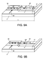
- a pole of the fixed magnet 30 (with reversible magnetization) is disposed in front of a pole of the magnet 30 '(with fixed magnetization) connected to the movable part (a planar element).
- This is connected to the substrate, by a hinge or a pivot 41, around which it will be able to pivot in the plane of the fixed substrate 2 or parallel to this plane.
- the field resulting from the fixed magnet magnet 30 ' will thus interact with the magnetic field of the fixed magnet, with reversible magnetization, in front of which it is located.
- the mobile element 4 undergoes a pair of electromagnetic forces induced by the magnets 30, 30 '(see Figure 9A ), the result of which is the pivoting indicated above.
- the Figure 9B corresponds to the case of a movable element in the form of a beam which supports the magnet with fixed magnetization. This again results in a bending motion around the end 41 of the beam fixed relative to the substrate 2, in one direction or the other, but always parallel to the surface 2 'of the substrate 2.
- Figures 8A - 9B allow to achieve a nano oscillator with magnetic actuation, with magnets with parallel magnetization and with reversal of the magnetic poles of one of the magnets.
- the magnet is made in the fixed substrate 2. This first example leads to the production of a device that operates according to the first mode of operation described above.
- a lithography step is followed, followed by dry etching of the oxide layer, stopping on the SiN layer.
- an etched area 230 is formed in which the magnet 30 will be formed ( figure 10D ).
- a deposition 27 of silicon nitride and a deposit 29 of a sacrificial layer, for example of oxide, with a thickness of about 50 nm are produced at low temperature ( figure 10G ).
- a sacrificial layer for example of oxide
- an SiO2 oxide deposit can be produced, followed by a Ti (sacrificial layer) deposit with release. of this layer by plasma XeF2. The thickness of the sacrificial layer will determine the "gap" between the mobile part and the fixed part.
- a layer 400 for example made of silicon nitride, is then deposited, in which the mobile beam can be formed ( figure 10H ).
- This layer is substantially 100 nm thick.
- a metal layer 160 for example an AlSi layer approximately 100 nm thick, is then deposited ( figure 10I ), in which the current lines 16 are made ( figure 10J ) by lithography and engraving.
- a lithography and etching step makes it possible to structure the mechanical element of the layer 400.
- the method can also be accompanied by a doping step to obtain good ohmic contacts under the connection pads of the current lines.
- the processes are carried out at low temperature ( ⁇ 250 ° C) from the deposition of the magnetic layers.
- Protective layers of the magnet can also be made to protect it during the release step.
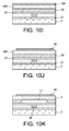
- the magnet is made on the movable element.
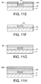
- a lithography and then a dry etching step of the oxide layer 23 is carried out, with stoppage on the layer 21 of SiN. Is thus achieved an engraved area 230 ( figure 11D ), in which will be / will be formed the current line or lines 16, by metal deposition or conductor 160, for example a deposit of 1 micron TiN ( figure 11E ). Alternatively, it is possible to proceed by electrolysis.
- a chemical-mechanical polishing with a stop on the oxide layer, makes it possible to eliminate the lateral portions 161, 162 of metallic or conductive deposits (on the non-etched areas of the layer 23) so as to leave only the portion forming the conductor 16 in the cavity 230 ( figure 11F ).
- a sacrificial layer 29, for example made of titanium, having a thickness of approximately 50 nm is deposited ( figure 11G ). The thickness of this sacrificial layer will determine the "gap" between the mobile part and the fixed part.
- a layer 400 for example a metal layer, of which an example is ruthenium (Ru), is then deposited, in which the mobile beam 4 can be formed ( figure 11H ).
- This layer is substantially 50 nm thick.
- Layers 300 of magnetic materials are then deposited ( figure 11I ), in which the magnet 30 is made ( figure 11J ) by lithography and ion etching.
- the beam 4 can then be lithographed and etched in the layer 400 ( figure 11K ).
- the sacrificial layer 29 is removed under the beam.
- the gap 17 between the mobile part 4 and the fixed part 2 is therefore released ( figure 11L ).
- an architecture is made with reciprocating the poles of the magnet.
- the current lines are made before the deposition of the magnetic layers.
- the first steps make it possible to obtain a structure identical to that of Figures 11A - 11E .
- the conductor obtained is that, 36, which will heat the magnetic structure 30 and to obtain the reversal of the field.
- the figure 12A therefore corresponds substantially to the structure obtained at the end of the figure 11F and on which is added an etch stop layer, for example a layer 27 of silicon nitride (SiN) of about 40 nm thick.
- an etch stop layer for example a layer 27 of silicon nitride (SiN) of about 40 nm thick.
- a layer 29 of oxide of thickness for example 100 nm, is deposited on the barrier layer.
- a lithography and then dry etching step of the oxide layer 29 is carried out, with stopping on the SiN layer.
- An etched area 290 is thus formed in which the magnet ( figure 12C ).
- a chemical-mechanical polishing with a stop on the nitride layer, makes it possible to eliminate the lateral portions 301, 302 of deposits of magnetic layers (on the non-etched areas of the layer 27) so as to leave only the portion forming the magnet 30 in the cavity 290 ( figure 12E ).
- a sacrificial layer 291 for example made of titanium, having a thickness of approximately 50 nm is deposited ( figure 12F ). The thickness of this sacrificial layer will determine the "gap" between the mobile part 4 and the fixed part 2.
- a layer 400 for example a metal layer, an example of which is ruthenium (Ru), is then deposited, in which the mobile beam can be formed ( figure 12F ).
- This layer is substantially 50 nm thick.
- the beam 4 can then be obtained by lithography and etching ( figure 12I ).
- the materials of the non-manufacturing layers of the magnet are chosen by way of example. It is also possible to add layers of protection of the magnets in order to preserve their integrities during the release. It is also possible to make two metal layers to structure two current lines, one for heating (by integrating a TiN or GeSbTe thermistor), the other inducing the reversal field (Cu for example).
Landscapes
- Physics & Mathematics (AREA)
- Acoustics & Sound (AREA)
- Condensed Matter Physics & Semiconductors (AREA)
- General Physics & Mathematics (AREA)
- Engineering & Computer Science (AREA)
- Manufacturing & Machinery (AREA)
- Micromachines (AREA)
- Piezo-Electric Or Mechanical Vibrators, Or Delay Or Filter Circuits (AREA)
Applications Claiming Priority (1)
| Application Number | Priority Date | Filing Date | Title |
|---|---|---|---|
| FR0852062A FR2929464B1 (fr) | 2008-03-28 | 2008-03-28 | Nano resonnateur magnetique |
Publications (2)
| Publication Number | Publication Date |
|---|---|
| EP2106024A1 true EP2106024A1 (de) | 2009-09-30 |
| EP2106024B1 EP2106024B1 (de) | 2018-02-07 |
Family
ID=39941520
Family Applications (1)
| Application Number | Title | Priority Date | Filing Date |
|---|---|---|---|
| EP09156165.4A Active EP2106024B1 (de) | 2008-03-28 | 2009-03-25 | Magnetischer Nano-Resonator |
Country Status (4)
| Country | Link |
|---|---|
| US (1) | US8310320B2 (de) |
| EP (1) | EP2106024B1 (de) |
| JP (1) | JP2009268084A (de) |
| FR (1) | FR2929464B1 (de) |
Cited By (1)
| Publication number | Priority date | Publication date | Assignee | Title |
|---|---|---|---|---|
| CN103728692A (zh) * | 2013-12-30 | 2014-04-16 | 清华大学 | 一种基于纳米梁结构的光机晶体微腔 |
Families Citing this family (18)
| Publication number | Priority date | Publication date | Assignee | Title |
|---|---|---|---|---|
| US7915973B2 (en) * | 2005-08-25 | 2011-03-29 | The Regents Of The University Of California | Tunable multiwalled nanotube resonator |
| FR2929443B1 (fr) * | 2008-03-28 | 2012-06-08 | Commissariat Energie Atomique | Nano-commutateur magnetique bistable |
| FR2948114B1 (fr) * | 2009-07-17 | 2012-03-30 | Commissariat Energie Atomique | Nems comportant des moyens de transduction a base d'alliage d'aluminium |
| FR2954512B1 (fr) * | 2009-12-21 | 2012-05-25 | Commissariat Energie Atomique | Realisation d'un dispositif a structures magnetiques formees sur un meme substrat et ayant des orientations d'aimantation respectives differentes |
| KR101099646B1 (ko) * | 2010-03-19 | 2011-12-29 | 연세대학교 산학협력단 | 나노공진기 제조방법 |
| KR101902267B1 (ko) | 2012-02-17 | 2018-09-28 | 삼성전자주식회사 | 나노 스케일 공진기, 나노 스케일 센서 및 이의 제조방법 |
| CN104470426B (zh) * | 2012-06-21 | 2021-05-25 | 皇家飞利浦有限公司 | 具有运动检测的磁共振检查系统 |
| KR101928344B1 (ko) | 2012-10-24 | 2018-12-13 | 삼성전자주식회사 | 나노 공진 장치 및 방법 |
| EP2784530B1 (de) * | 2013-03-27 | 2016-03-02 | IMEC vzw | Zweiachsiges MEMS-Resonanzmagnetometer |
| FR3017463B1 (fr) | 2014-02-13 | 2020-11-13 | Commissariat Energie Atomique | Capteur de concentration de gaz a structure suspendue |
| TWI531805B (zh) * | 2014-09-18 | 2016-05-01 | 碩英股份有限公司 | 磁力計 |
| FR3054364B1 (fr) | 2016-07-20 | 2018-08-17 | Commissariat A L'energie Atomique Et Aux Energies Alternatives | Aimant permanent comprenant un empilement de n motifs |
| FR3073661B1 (fr) | 2017-11-10 | 2019-11-22 | Commissariat A L'energie Atomique Et Aux Energies Alternatives | Aimant permanent comprenant une couche antiferromagnetique et une couche ferromagnetique |
| WO2020006008A1 (en) * | 2018-06-26 | 2020-01-02 | Magic Leap, Inc. | Raster scanned projector with microelectromechanical system scanner |
| WO2020006011A1 (en) | 2018-06-26 | 2020-01-02 | Magic Leap, Inc. | Hybrid optical fiber mems scanner |
| US10615887B1 (en) * | 2018-09-24 | 2020-04-07 | Seagate Technology Llc | Mitigation of noise generated by random excitation of asymmetric oscillation modes |
| US20230420548A1 (en) * | 2022-06-24 | 2023-12-28 | International Business Machines Corporation | Magnetic structures for resonant manipulation of spin |
| DE102023109183A1 (de) * | 2023-04-12 | 2024-10-17 | eleQtron GmbH | Elektrischer Leiter und Verfahren zur Herstellung eines elektrischen Leiters |
Citations (3)
| Publication number | Priority date | Publication date | Assignee | Title |
|---|---|---|---|---|
| US6593731B1 (en) * | 1999-07-08 | 2003-07-15 | California Institute Of Technology | Displacement transducer utilizing miniaturized magnet and hall junction |
| WO2003061470A1 (en) * | 2002-01-18 | 2003-07-31 | California Institute Of Technology | Method and apparatus for nanomagnetic manipulation and sensing |
| WO2006076037A2 (en) * | 2004-05-24 | 2006-07-20 | Trustees Of Boston University | Controllable nanomechanical memory element |
Family Cites Families (21)
| Publication number | Priority date | Publication date | Assignee | Title |
|---|---|---|---|---|
| NL7907115A (nl) * | 1979-09-25 | 1981-03-27 | Philips Nv | Werkwijze voor het vervaardigen van een permanente magneet ter plaatsing in een luchtspleet van een transformatorkern. |
| US6188504B1 (en) * | 1996-06-28 | 2001-02-13 | Olympus Optical Co., Ltd. | Optical scanner |
| US5963857A (en) * | 1998-01-20 | 1999-10-05 | Lucent Technologies, Inc. | Article comprising a micro-machined filter |
| US6346189B1 (en) * | 1998-08-14 | 2002-02-12 | The Board Of Trustees Of The Leland Stanford Junior University | Carbon nanotube structures made using catalyst islands |
| JP3811304B2 (ja) * | 1998-11-25 | 2006-08-16 | 株式会社日立製作所 | 変位センサおよびその製造方法 |
| FR2811163B1 (fr) * | 2000-06-30 | 2002-10-04 | Centre Nat Rech Scient | Filtre nono-electromecanique |
| EP1197726A1 (de) * | 2000-10-04 | 2002-04-17 | Eidgenössische Technische Hochschule Zürich | Multifunktion-Sensor und Hebel dafür |
| US6495905B2 (en) * | 2000-11-09 | 2002-12-17 | Texas Instruments Incorporated | Nanomechanical switches and circuits |
| RU2181901C1 (ru) * | 2001-01-19 | 2002-04-27 | Акционерное общество закрытого типа Научно-производственная фирма по геофизическим и геоэкологическим работам "КАРОТАЖ" | Способ каротажа с использованием ядерно-магнитного резонанса и устройство для его осуществления |
| US6835926B2 (en) * | 2001-04-12 | 2004-12-28 | California Institute Of Technology | Mechanical sensors of electromagnetic fields |
| WO2002088764A1 (en) * | 2001-04-26 | 2002-11-07 | The Johns Hopkins University | Lorentz force driven mechanical filter/mixer designs for rf applications |
| US7191639B2 (en) * | 2003-04-08 | 2007-03-20 | California Institute Of Technology | On-chip magnetic force actuation of microcantilevers by coplanar coils |
| JP4593239B2 (ja) * | 2003-11-19 | 2010-12-08 | パナソニック株式会社 | 電気機械フィルタ |
| JP4611127B2 (ja) * | 2004-06-14 | 2011-01-12 | パナソニック株式会社 | 電気機械信号選択素子 |
| CN100570429C (zh) * | 2004-06-24 | 2009-12-16 | 康乃尔研究基金会有限公司 | 基于纤维复合材料的mems光扫描器 |
| KR100653083B1 (ko) * | 2004-12-27 | 2006-12-01 | 삼성전자주식회사 | Rf 스위치 |
| US7915973B2 (en) * | 2005-08-25 | 2011-03-29 | The Regents Of The University Of California | Tunable multiwalled nanotube resonator |
| JP4599256B2 (ja) * | 2005-09-09 | 2010-12-15 | 株式会社東芝 | 磁気スイッチング素子及びこれを用いた信号処理装置 |
| US7642692B1 (en) * | 2005-09-15 | 2010-01-05 | The United States Of America As Represented By The Secretary Of The Army | PZT MEMS resonant Lorentz force magnetometer |
| KR101336962B1 (ko) * | 2007-06-01 | 2013-12-04 | 삼성전자주식회사 | 복합 구조의 빔을 이용한 나노 공진기 |
| US7471083B1 (en) * | 2008-01-10 | 2008-12-30 | Joshi Ramesh L | Apparatus and method for showing that a magnetic field produces a couple and not a force |
-
2008
- 2008-03-28 FR FR0852062A patent/FR2929464B1/fr not_active Expired - Fee Related
-
2009
- 2009-03-25 EP EP09156165.4A patent/EP2106024B1/de active Active
- 2009-03-27 JP JP2009080292A patent/JP2009268084A/ja active Pending
- 2009-03-27 US US12/412,865 patent/US8310320B2/en active Active
Patent Citations (3)
| Publication number | Priority date | Publication date | Assignee | Title |
|---|---|---|---|---|
| US6593731B1 (en) * | 1999-07-08 | 2003-07-15 | California Institute Of Technology | Displacement transducer utilizing miniaturized magnet and hall junction |
| WO2003061470A1 (en) * | 2002-01-18 | 2003-07-31 | California Institute Of Technology | Method and apparatus for nanomagnetic manipulation and sensing |
| WO2006076037A2 (en) * | 2004-05-24 | 2006-07-20 | Trustees Of Boston University | Controllable nanomechanical memory element |
Non-Patent Citations (1)
| Title |
|---|
| ROOKES ET AL., APPLIED PHYSICS LETTERS, vol. 84, no. 22, 2004 |
Cited By (1)
| Publication number | Priority date | Publication date | Assignee | Title |
|---|---|---|---|---|
| CN103728692A (zh) * | 2013-12-30 | 2014-04-16 | 清华大学 | 一种基于纳米梁结构的光机晶体微腔 |
Also Published As
| Publication number | Publication date |
|---|---|
| JP2009268084A (ja) | 2009-11-12 |
| FR2929464B1 (fr) | 2011-09-09 |
| US20090289747A1 (en) | 2009-11-26 |
| EP2106024B1 (de) | 2018-02-07 |
| US8310320B2 (en) | 2012-11-13 |
| FR2929464A1 (fr) | 2009-10-02 |
Similar Documents
| Publication | Publication Date | Title |
|---|---|---|
| EP2106024B1 (de) | Magnetischer Nano-Resonator | |
| EP2592429B1 (de) | Vektorieller Magnetfeldsensor | |
| US8174352B2 (en) | Method for making a transducer, transducer made therefrom, and applications thereof | |
| FR2892871A1 (fr) | Oscillateur radio frequence a courant elelctrique polarise en spin | |
| EP1286465A1 (de) | Mikroelektromechanisches Bauelement | |
| EP1428232B8 (de) | Mobilmagnetbetätigungsglied | |
| EP2616386A1 (de) | In der ebene betätigte resonanzvorrichtung und verfahren zur herstellung der vorrichtung | |
| EP3159300B1 (de) | Mikroelektromechanische und/oder nanoelektromechanische struktur mit mindestens zwei unterschiedlich polarisierten thermischen aktuatoren | |
| CH656010A5 (fr) | Dispositif miniature sensible au champ magnetique et appareil de mesure du champ magnetique comportant un tel dispositif. | |
| EP2105940B1 (de) | Bistabiler magnetischer Nano-Schalter | |
| FR2984010A1 (fr) | Dispositif capacitif integre ayant une valeur capacitive thermiquement variable | |
| EP2194544A1 (de) | Hochfrequenzoszillator basierend auf Drehventilen oder Tunnelübergängen | |
| EP2580766A1 (de) | Spinübertragungsoszillator | |
| FR3066854B1 (fr) | Dispositif magnetique integre a inductance variable et procede de realisation d'un tel dispositif | |
| EP1836714B1 (de) | Mikrosystem mit elektromagnetischer steuerung | |
| EP2597655B1 (de) | Herstellungsverfahren einer Vorrichtung enthaltend mehrere magnetische Einheiten in verschiedene Richtungen magnetisiert | |
| US10553786B2 (en) | Magneto-resistance device including conjugated molecule | |
| FR3057958A1 (fr) | Sonde pour microscopie a force atomique miniaturisee et a faible encombrement | |
| EP2201681A1 (de) | Auf nanometrischem oder mikrometrischem massstab vibrierende elektromechanische komponente mit verbessertem detektionsniveau | |
| EP1846320B1 (de) | Mikromechanische vorrichtung mit einem beweglichen balken | |
| EP4564078A1 (de) | Magnetisch betätigte reflektorvorrichtung und verfahren dafür | |
| WO2013186383A1 (fr) | Capteur de champ magnetique a force de laplace | |
| EP3159703A1 (de) | Mikroelektromechanische vorrichtung und system mit einem wandler mit einer schwachen impedanz | |
| FR2880730A1 (fr) | Microsysteme utilisant un microactionneur magnetique a aimant permanent. | |
| EP1836713B1 (de) | Mikrosystem mit integrierter rückhaltemagnetschaltung |
Legal Events
| Date | Code | Title | Description |
|---|---|---|---|
| PUAI | Public reference made under article 153(3) epc to a published international application that has entered the european phase |
Free format text: ORIGINAL CODE: 0009012 |
|
| AK | Designated contracting states |
Kind code of ref document: A1 Designated state(s): AT BE BG CH CY CZ DE DK EE ES FI FR GB GR HR HU IE IS IT LI LT LU LV MC MK MT NL NO PL PT RO SE SI SK TR |
|
| AX | Request for extension of the european patent |
Extension state: AL BA RS |
|
| 17P | Request for examination filed |
Effective date: 20100223 |
|
| RAP1 | Party data changed (applicant data changed or rights of an application transferred) |
Owner name: COMMISSARIAT A L'ENERGIE ATOMIQUE ET AUX ENERGIES |
|
| AKX | Designation fees paid |
Designated state(s): DE FR GB IT |
|
| 17Q | First examination report despatched |
Effective date: 20160630 |
|
| GRAP | Despatch of communication of intention to grant a patent |
Free format text: ORIGINAL CODE: EPIDOSNIGR1 |
|
| STAA | Information on the status of an ep patent application or granted ep patent |
Free format text: STATUS: GRANT OF PATENT IS INTENDED |
|
| RIC1 | Information provided on ipc code assigned before grant |
Ipc: G01R 33/028 20060101ALN20170109BHEP Ipc: H03H 9/24 20060101AFI20170109BHEP Ipc: H03H 9/02 20060101ALI20170109BHEP Ipc: H03H 3/007 20060101ALI20170109BHEP |
|
| INTG | Intention to grant announced |
Effective date: 20170209 |
|
| GRAS | Grant fee paid |
Free format text: ORIGINAL CODE: EPIDOSNIGR3 |
|
| GRAJ | Information related to disapproval of communication of intention to grant by the applicant or resumption of examination proceedings by the epo deleted |
Free format text: ORIGINAL CODE: EPIDOSDIGR1 |
|
| GRAL | Information related to payment of fee for publishing/printing deleted |
Free format text: ORIGINAL CODE: EPIDOSDIGR3 |
|
| STAA | Information on the status of an ep patent application or granted ep patent |
Free format text: STATUS: EXAMINATION IS IN PROGRESS |
|
| GRAP | Despatch of communication of intention to grant a patent |
Free format text: ORIGINAL CODE: EPIDOSNIGR1 |
|
| STAA | Information on the status of an ep patent application or granted ep patent |
Free format text: STATUS: GRANT OF PATENT IS INTENDED |
|
| INTC | Intention to grant announced (deleted) | ||
| RIC1 | Information provided on ipc code assigned before grant |
Ipc: H03H 9/02 20060101ALI20170620BHEP Ipc: H03H 3/007 20060101ALI20170620BHEP Ipc: G01R 33/028 20060101ALN20170620BHEP Ipc: H03H 9/24 20060101AFI20170620BHEP |
|
| INTG | Intention to grant announced |
Effective date: 20170710 |
|
| GRAJ | Information related to disapproval of communication of intention to grant by the applicant or resumption of examination proceedings by the epo deleted |
Free format text: ORIGINAL CODE: EPIDOSDIGR1 |
|
| GRAL | Information related to payment of fee for publishing/printing deleted |
Free format text: ORIGINAL CODE: EPIDOSDIGR3 |
|
| STAA | Information on the status of an ep patent application or granted ep patent |
Free format text: STATUS: EXAMINATION IS IN PROGRESS |
|
| INTC | Intention to grant announced (deleted) | ||
| RIC1 | Information provided on ipc code assigned before grant |
Ipc: H03H 9/02 20060101ALI20171115BHEP Ipc: G01R 33/028 20060101ALN20171115BHEP Ipc: H03H 9/24 20060101AFI20171115BHEP Ipc: H03H 3/007 20060101ALI20171115BHEP |
|
| GRAR | Information related to intention to grant a patent recorded |
Free format text: ORIGINAL CODE: EPIDOSNIGR71 |
|
| STAA | Information on the status of an ep patent application or granted ep patent |
Free format text: STATUS: GRANT OF PATENT IS INTENDED |
|
| GRAA | (expected) grant |
Free format text: ORIGINAL CODE: 0009210 |
|
| STAA | Information on the status of an ep patent application or granted ep patent |
Free format text: STATUS: THE PATENT HAS BEEN GRANTED |
|
| RIC1 | Information provided on ipc code assigned before grant |
Ipc: H03H 3/007 20060101ALI20171214BHEP Ipc: H03H 9/02 20060101ALI20171214BHEP Ipc: G01R 33/028 20060101ALN20171214BHEP Ipc: H03H 9/24 20060101AFI20171214BHEP |
|
| INTG | Intention to grant announced |
Effective date: 20171222 |
|
| AK | Designated contracting states |
Kind code of ref document: B1 Designated state(s): DE FR GB IT |
|
| REG | Reference to a national code |
Ref country code: GB Ref legal event code: FG4D Free format text: NOT ENGLISH |
|
| REG | Reference to a national code |
Ref country code: DE Ref legal event code: R096 Ref document number: 602009050670 Country of ref document: DE |
|
| REG | Reference to a national code |
Ref country code: FR Ref legal event code: PLFP Year of fee payment: 10 |
|
| PG25 | Lapsed in a contracting state [announced via postgrant information from national office to epo] |
Ref country code: IT Free format text: LAPSE BECAUSE OF FAILURE TO SUBMIT A TRANSLATION OF THE DESCRIPTION OR TO PAY THE FEE WITHIN THE PRESCRIBED TIME-LIMIT Effective date: 20180207 |
|
| REG | Reference to a national code |
Ref country code: DE Ref legal event code: R097 Ref document number: 602009050670 Country of ref document: DE |
|
| PLBE | No opposition filed within time limit |
Free format text: ORIGINAL CODE: 0009261 |
|
| STAA | Information on the status of an ep patent application or granted ep patent |
Free format text: STATUS: NO OPPOSITION FILED WITHIN TIME LIMIT |
|
| 26N | No opposition filed |
Effective date: 20181108 |
|
| PGFP | Annual fee paid to national office [announced via postgrant information from national office to epo] |
Ref country code: GB Payment date: 20260324 Year of fee payment: 18 |
|
| PGFP | Annual fee paid to national office [announced via postgrant information from national office to epo] |
Ref country code: DE Payment date: 20260320 Year of fee payment: 18 |
|
| PGFP | Annual fee paid to national office [announced via postgrant information from national office to epo] |
Ref country code: FR Payment date: 20260324 Year of fee payment: 18 |