EP2106123A2 - Procédé de commande d'un détecteur à rayons X et détecteur à rayons X l'utilisant - Google Patents
Procédé de commande d'un détecteur à rayons X et détecteur à rayons X l'utilisant Download PDFInfo
- Publication number
- EP2106123A2 EP2106123A2 EP09000631A EP09000631A EP2106123A2 EP 2106123 A2 EP2106123 A2 EP 2106123A2 EP 09000631 A EP09000631 A EP 09000631A EP 09000631 A EP09000631 A EP 09000631A EP 2106123 A2 EP2106123 A2 EP 2106123A2
- Authority
- EP
- European Patent Office
- Prior art keywords
- period
- gate
- ray
- during
- signal
- Prior art date
- Legal status (The legal status is an assumption and is not a legal conclusion. Google has not performed a legal analysis and makes no representation as to the accuracy of the status listed.)
- Withdrawn
Links
Images

Classifications
-
- G—PHYSICS
- G01—MEASURING; TESTING
- G01T—MEASUREMENT OF NUCLEAR OR X-RADIATION
- G01T1/00—Measuring X-radiation, gamma radiation, corpuscular radiation, or cosmic radiation
- G01T1/16—Measuring radiation intensity
- G01T1/24—Measuring radiation intensity with semiconductor detectors
-
- H—ELECTRICITY
- H04—ELECTRIC COMMUNICATION TECHNIQUE
- H04N—PICTORIAL COMMUNICATION, e.g. TELEVISION
- H04N23/00—Cameras or camera modules comprising electronic image sensors; Control thereof
- H04N23/80—Camera processing pipelines; Components thereof
- H04N23/81—Camera processing pipelines; Components thereof for suppressing or minimising disturbance in the image signal generation
-
- G—PHYSICS
- G01—MEASURING; TESTING
- G01T—MEASUREMENT OF NUCLEAR OR X-RADIATION
- G01T1/00—Measuring X-radiation, gamma radiation, corpuscular radiation, or cosmic radiation
-
- H—ELECTRICITY
- H04—ELECTRIC COMMUNICATION TECHNIQUE
- H04N—PICTORIAL COMMUNICATION, e.g. TELEVISION
- H04N23/00—Cameras or camera modules comprising electronic image sensors; Control thereof
- H04N23/30—Cameras or camera modules comprising electronic image sensors; Control thereof for generating image signals from X-rays
-
- H—ELECTRICITY
- H04—ELECTRIC COMMUNICATION TECHNIQUE
- H04N—PICTORIAL COMMUNICATION, e.g. TELEVISION
- H04N25/00—Circuitry of solid-state image sensors [SSIS]; Control thereof
- H04N25/30—Circuitry of solid-state image sensors [SSIS]; Control thereof for transforming X-rays into image signals
Definitions
- the present invention relates to a method of driving an x-ray detector and an x-ray detector using the same. More particularly, the present invention relates to an x-ray detector and a method of driving the x-ray detector in which image distortion caused by an offset voltage deviation is substantially reduced and/or effectively prevented.
- An x-ray detector is used, for example, as a medical diagnosis device which detects an x-ray image of an object photographed by an x-ray generator, to provide the x-ray image to a display device.
- a flat panel x-ray detector using the DR method typically includes a plurality of light detecting pixels in the flat panel detector to detect an x-ray incident thereon.
- Each light detecting pixel of the plurality of light detecting pixels includes a photodiode.
- the photodiode detects an x-ray emitted from an x-ray generator and outputs an electrical signal proportional to the x-ray.
- the light detecting pixel further includes a switching device which transmits the electrical signal output from the photodiode to a readout integrated circuit of the flat panel x-ray detector.
- the readout integrated circuit reads out, e.g., receives, the electrical signal from the flat panel detector. Specifically, the readout integrated circuit reads out the electrical signal based on a gate voltage provided from a gate driver which sequentially turns on switching devices of associated light detecting pixels arranged in a row direction. Thus, the readout integrated circuit sequentially reads out electrical signals on a row basis.
- the electrical signal is thereafter output from the readout integrated circuit and is processed in a controller, typically disposed on a main board.
- the electrical signal is thereafter converted to an image signal and transmitted to a display device to display the x-ray image thereon.
- an electric potential at a coupling node e.g., a node at which the photodiode and the switching device of a given light detecting pixel are connected
- an input interval e.g., a duty cycle
- an operation timing of the photo diode changes and, as a result, the offset voltage at the coupling node further varies.
- the electrical signal output from the photodiode is adversely affected.
- a distortion in which the offset voltage is added to the electrical signal when the switching device is turned on may occur.
- an offset compensation method which detects the offset voltage of the signal output from the switching device to remove the offset voltage from the electrical signal.
- the offset compensation method of the prior art when the offset voltage varies based on the operation timing of the photo diode, as described above, it is difficult to perform the offset compensation method.
- a distorted image, caused by an offset voltage deviation based on the operation timing of the photo diode is displayed on the display device of the x-ray detector of the prior art.
- Exemplary embodiments of the present invention provide a method of driving an x-ray detector in which image distortion caused by an offset voltage deviation is effectively prevented.
- Exemplary embodiments of the present invention also provide an x-ray detector using the driving method in which the image distortion caused by the offset voltage deviation is effectively prevented.
- an x-ray detector includes an x-ray generator which emits an x-ray and a light detecting pixel.
- the light detecting pixel includes a photodiode which detects the x-ray emitted from the x-ray generator during an x-ray detecting period, and outputs an electrical signal corresponding to the x-ray.
- the light detecting pixel further includes a switching device connected to the photodiode.
- the x-ray detector further includes a light-generating sheet which provides a light to the photodiode during a first flash period of an offset control period, a gate driver which outputs a gate signal to the switching device, and a read-out circuit which receives a signal output from an output terminal of the switching device.
- the gate signal includes a first gate turn-on signal which turns on the switching device during a first gate turn-on period of the x-ray detecting period, and a second gate turn-on signal which turns on the switching device during a second gate turn-on period of the offset control period.
- a method of driving an x-ray detector includes a switching device connected to a light detecting pixel comprising a photodiode which detects an x-ray emitted from an x-ray generator during an x-ray detecting period and outputs an electrical signal corresponding to the x-ray.
- the method includes: receiving the x-ray from the x-ray generator with the photodiode during the x-ray detecting period to generate the electrical signal corresponding to the x-ray; turning on the switching device during a first gate turn-on period of the x-ray detecting period to transmit the electrical signal to an external component; providing a light to the photodiode during an offset control period after the x-ray detecting period; and turning on the switching device during a second gate turn-on period of the offset control period during which the light is not provided to the photodiode to maintain an electric potential at a coupling node disposed between the photodiode and the switching device at a predetermined level.
- an electric potential at a coupling node of a photodiode and a switching device is uniformly maintained at a predetermined level, thereby preventing image distortion caused by an offset voltage deviation.
- first,” “second,” “third” etc. may be used herein to describe various elements, components, regions, layers and/or sections, these elements, components, regions, layers and/or sections should not be limited by these terms. These terms are only used to distinguish one element, component, region, layer or section from another element, component, region, layer or section. Thus, a first element, component, region, layer or section discussed below could be termed a second element, component, region, layer or section without departing from the teachings of the present invention.
- relative terms such as “lower” or “bottom” and “upper” or “top” may be used herein to describe one element's relationship to other elements as illustrated in the Figures. It will be understood that relative terms are intended to encompass different orientations of the device in addition to the orientation depicted in the Figures. For example, if the device in one of the figures is turned over, elements described as being on the “lower” side of other elements would then be oriented on the “upper” side of the other elements. The exemplary term “lower” can, therefore, encompass both an orientation of “lower” and “upper,” depending upon the particular orientation of the figure.
- Exemplary embodiments of the present invention are described herein with reference to cross section illustrations which are schematic illustrations of idealized embodiments of the present invention. As such, variations from the shapes of the illustrations as a result, for example, of manufacturing techniques and/or tolerances, are to be expected. Thus, embodiments of the present invention should not be construed as limited to the particular shapes of regions illustrated herein but are to include deviations in shapes which result, for example, from manufacturing. For example, a region illustrated or described as flat may, typically, have rough and/or nonlinear features. Moreover, sharp angles which are illustrated may be rounded. Thus, the regions illustrated in the figures are schematic in nature and their shapes are not intended to illustrate the precise shape of a region and are not intended to limit the scope of the present invention.
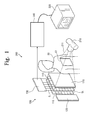
- FIG. 1 is a view showing an exemplary embodiment of an X-ray system.
- an X-ray system 200 includes an X-ray generator 210 that generates X-rays 211 in a direction toward a predetermined region 51 of a patient 50 (that is, an inspection region), an X-ray detector 100 that detects X-rays 211 which have passed through the predetermined region 51 of the patient 50, and a display apparatus 220 that displays an image by receiving image signals corresponding to the X-rays 211 detected by the X-ray detector 100.
- an X-ray system 200 is described with respect to the imaging of a patient 50, it would be clear to one of ordinary skill in the art that such an exemplary embodiment of an X-ray system 200 may be applied to a wide range of applications wherein X-ray imaging is desired, e.g., luggage inspection, etc.
- the scintillator 170 provided between a flat panel 110 of the X-ray detector 100 and the patient 50 converts the X-ray 211, which has passed through the patient 50, into green light to provide the green light to the flat panel 110.
- the X-ray detector 100 may be described in detail with reference to FIG. 2 .
- the X-ray detector 100 obtains image signals corresponding to X-rays 211, which have passed through the patient 50, and then provides the image signal to the display apparatus 220. Accordingly, the display apparatus 220 may display the X-ray images corresponding to the image signals in real time. As an example of the present invention, the display apparatus 220 may include a liquid crystal display (“LCD”), and various other display types as would be known to one of ordinary skill in the art.
- LCD liquid crystal display
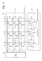
- FIG. 2 is a schematic circuit diagram of an x-ray detector according to an exemplary embodiment the present invention shown in FIG. 1 .
- an x-ray detector 100 includes a flat panel 110 which includes a plurality of light detecting pixels PP.
- Each light detecting pixel PP of the plurality of light detecting pixels PP detects an x-ray emitted from an x-ray generator 210 ( FIG 1 ) and photoelectrically converts the detected x-ray to output an electrical signal proportional to the detected x-ray.
- the flat panel 110 further includes gate lines GL which extend substantially in parallel with each other in a first direction, e.g., a row direction, and data lines DL which extend substantially in parallel with each other in a second direction perpendicular to the first direction, e.g., in a column direction.
- a plurality of areas is formed in a substantially matrix configuration by the gate lines GL and the data lines DL in the flat panel 110, and the light detecting pixels PP are disposed in respective areas of the plurality of areas.
- a first gate line GL1, a second gate line GL2 and a third gate line GL3, as well as a first data line DL1, a second data line DL2 and a third data line DL3 are shown, but alternative exemplary embodiments are not limited thereto.
- the areas include one of the light detecting pixels PP, and each of the light detecting pixels PP includes a photodiode PD and a transistor Tr.
- the photodiode PD detects an x-ray emitted from an x-ray generator 210 and converts the detected x-ray into an electrical signal to output the electrical signal.
- the photodiode PD includes a first electrode connected to an input electrode of the transistor Tr and a second electrode connected to a bias line BL to which a bias voltage Vbias is applied.
- the bias voltage Vbias has a voltage level in a range of approximately -5V to approximately -10V.
- the bias voltage Vbias reverse biases the photodiode PD and, more particularly maintains the photodiode PD in a reverse bias state, as will be described below with reference to FIGS. 3 and 4 .
- a control electrode of the transistor Tr is electrically connected to a gate driver 120 through a corresponding gate line GL, and an output electrode of the transistor Tr is electrically connected to a readout integrated circuit 130 through a corresponding data line DL.
- a node to which the first electrode of the photodiode PD and the input electrode of the transistor Tr are connected is referred to as a coupling node N 1.
- each light detecting pixel PP includes an associated coupling node N1 disposed between the photodiode PD and the transistor Tr associated therewith.
- the gate driver 120 generates a gate signal and sequentially applies the gate signal to the first, second and third gate lines GL1, GL2 and GL3, respectively.
- the gate signal is a voltage signal and swings between a gate-on voltage which turns on the transistor Tr and a gate-off voltage which turns off the transistor Tr.
- the gate-on voltage has a voltage level of approximately 15V
- the gate-off voltage has a voltage level of approximately -10V, but alternative exemplary embodiments are not limited thereto.
- the electrical signal output from the photodiode PD is applied to a corresponding data line DL through the turned-on transistor Tr. Therefore, the data line DL transmits the electrical signal output from the transistor Tr to the readout integrated circuit 130. Further, since the light detecting pixels PP are turned on row by row in response to the gate signal sequentially supplied to the gate lines GL from the gate driver 120, the electrical signal is transmitted to the readout integrated circuit 130 on a row by row basis, e.g., based on the gate signal.
- the readout integrated circuit 130 includes a plurality of amplifiers 131a, 131b and 131c and, more specifically, a first amplifier 131a, a second amplifier 131a and a third amplifier 131c connected to the first data line DL1, the second data line DL2 and the third data line DL3, respectively, as shown in FIG. 2 .
- the readout integrated circuit 130 includes a multiplexer 132 connected to respective output terminals of the plurality of amplifiers 131a, 131b and 131c.
- the first, second and third amplifiers 131a, 131b and 131c, respectively is an operational amplifier ("OP AMP"), but alternative exemplary embodiments are not limited thereto.
- OP AMP operational amplifier
- a negative input terminal ("-") of each of the first, second and third amplifiers 131a, 131b and 131c, respectively, is connected to a corresponding data line DL, e.g., to the first data line DL1, the second data line DL2 and the third data line DL3, respectively, to receive the electrical signal output from a corresponding light detecting pixel PP, and a positive input terminal ("+") of each of the first, second and third amplifiers 131a, 131b and 131c, respectively, receives a reference voltage.
- the reference voltage is a ground voltage.
- first, second and third capacitors C1, C2, and C3, respectively, are connected between the negative input terminal (-) and an output terminal of each of the first amplifier 131a, the second amplifier 131 b and the third amplifier 131c.
- Input terminals of the multiplexer 132 are connected to corresponding output terminals of each of the first, second and third amplifiers 131a, 131b and 131c, respectively, to receive a signal output therefrom.
- a signal OUT output from the multiplexer 132 is applied to a control circuit (not shown) arranged on a main board, for example, of the x-ray detector 100 and is converted to a digital signal by an analog-to-digital converter (not shown) in the control circuit.
- the digital signal is transmitted as an image signal to a display device 220 ( FIG 1 ) connected to the x-ray detector 100.
- the display device displays an x-ray image corresponding to the image signal provided from the x-ray detector 100 on a screen of the display device.
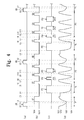
- FIGS. 3a to 3d are signal timing diagrams illustrating waveforms of an x-ray detector according to an exemplary embodiment of the present invention. More specifically, FIG. 3a is a signal timing diagram showing when an x-ray is provided to the photodiode PD of the x-ray detector 100 according to an exemplary embodiment, FIG. 3b is a signal timing diagram showing when a gate signal is applied to the gate line GL of the x-ray detector 100, FIG. 3b is a signal timing diagram showing when a light is provided from a light generating sheet 115 ( FIG 1 ) of the x-ray detector, and FIG. 3d is a signal timing diagram showing an electric potential at the coupling node N1 of the x-ray detector 100.
- a driving period of the x-ray detector 100 (best shown in FIG. 2 ) includes an x-ray detecting period PI, a signal deleting period PE, and an offset control period P0.
- the x-ray detecting period PI includes a period during which an x-ray, generated during an x-ray generating period XR, from the x-ray generator is received by the light detecting pixel pp ( FIG. 2 ) and an electrical signal corresponding to the x-ray generated during the x-ray generating period XR is generated.
- the photodiode PD ( FIG. 2 ) is biased in a forward direction, and an electric potential at the coupling node N1 to which the photodiode PD and the transistor Tr are connected decreases from a first voltage VA1 at which the coupling node N1 is at the beginning of the x-ray detecting period PI.
- the first voltage VA1 is an initial voltage of the coupling node N1.
- the electric potential at the coupling node N1 decreases to a second voltage VA2 until a first time point t1, at which the generation of the x-ray is stopped, e.g., until the end of the x-ray generating period XR of the x-ray detecting period PI.
- the gate signal applied to the control electrode of the transistor Tr transitions from the gate-off voltage Voff to the gate-on voltage Von at a second time point t2.
- the transistor Tr is turned on (in response to the gate-on voltage Von) during a first gate-on period GE between the second time point t2 and a third time point t3, e.g., during a time period in which the gate signal is maintained at the gate-on voltage Von.
- the electric potential at the coupling node N1 gradually increases back to the first voltage VA1, as shown in FIG. 3d .
- the transistor Tr is turned off at the third time point t3, when the gate signal transitions to the gate-off voltage Voff, and the electric potential at the coupling node N1 is thereby lowered to a third voltage VA3.
- the third voltage VA3 is less than the first voltage VA1 but greater than the second voltage VA2. Since the transistor Tr is turned off at the third time point t3, the electric potential at the coupling node N1 is maintained at the third voltage VA3, as shown in FIG. 3d . Therefore, the x-ray detecting period PI is substantially defined as being from the initial time point t0 to the third time point t3.
- the signal deleting period PE which is a period in which the electric potential charged to the coupling node N1 during the x-ray detecting period PI is removed such that the electric potential at the coupling node N1 returns to an initial state, thereby effectively preventing a previous signal, e.g., a previous signal from the light detecting pixel PP, from affecting, e.g., interfering with and/or mixing with, a next signal.
- the signal deleting period PE begins at a fourth time point t4, at which time the light generating sheet (not shown) generates a light which saturates the photodiode PD, as shown in FIG. 3c .
- the light generating sheet includes an inorganic light emitting material and therewith provides the light to the flat panel 110 ( FIG. 2 ) of the x-ray detector 100 during a second flash period FE.
- the photodiode PD is again biased in the forward direction, and the electric potential at the coupling node N1 decreases to a fourth voltage VA4 until a fifth time point t5 at which the supply of the light is stopped, as shown in FIG. 3c .
- the electric potential at the coupling node N1 is maintained at the fourth voltage VA4 until a sixth time point t6.
- the gate signal transitions to the gate-on voltage Von, and the transistor Tr is turned on during a third gate-on period GT between the sixth time point t6 and a seventh time point t7, as shown in FIG. 3b .
- the electric potential at the coupling node N1 thereby increases back to the first voltage VA1 during the third gate-on period GT. Therefore, a previous signal is completely removed from the coupling node N1, and the electric potential at the coupling node N1 is thereby initialized.
- the signal deleting period PE is defined from the fourth time point t4 to the seventh time point t7.
- the offset control period P0 begins after the signal deleting period PE.
- the offset control period P0 includes at least one first flash period F0 during, which the light is generated by the light generating sheet, and at least one second gate-on period G0, during which the gate signal is at the gate-on voltage to turn on the transistor Tr. More specifically, the first flash period F0 is maintained during a time interval in which the photodiode PD ( FIG. 2 ) is saturated and the second gate-on period G0, during which the gate signal transitions to the gate-on voltage Von after the first flash period F0.
- the first flash period F0 and/or the second gate-on period G0 may occur more than once, e.g., repeatedly, during a single offset control period P0.
- the first flash periods F0 may have a same time width dt, e.g., a duration dt, but alternative exemplary embodiments are not limited thereto.
- durations of the first flash periods F0 and/or the second gate-on periods G0 may be varied, as will be described in further detail below with reference to FIG. 4 .
- the electric potential at the coupling node N1 decreases between an eighth time point t8, at which the first flash period F0 begins, and is eventually lowered to the fourth voltage VA4 at a ninth time point t9, at which the first flash period F0 is finished. Then, the second gate-on period G0 begins at a tenth time point t10 at which the gate signal transitions to the gate-on voltage Von, as shown in FIG. 3b .
- the electric potential at the coupling node N1 increases during the second gate-on period G0 and reaches the first voltage VA1 at an eleventh time point t11, e.g., at a time point at which the second gate-on period G0 ends.
- the electric potential at the coupling node N1 is uniformly maintained at the first voltage VA1 even when the second gate-on period G0 is removed, since the first flash period F0 and the second gate-on period G0 occur.
- the offset control period P0 is therefore defined as being from the eighth time point t8, at which the light, e.g., an optical flash, is generated, to a subsequent initial time point t0, e.g., when a next x-ray is generated in the next x-ray generating period XR.
- the electric potential at the coupling node N1 of the x-ray detector 100 is uniformly maintained at the first voltage VA1 at the initial time point t0 when the next x-ray is generated in the offset control period P0. Therefore, an offset voltage deviation is substantially reduced and/or effectively prevented in the x-ray detector 100 according to an exemplary embodiment.
- FIGS. 4a to 4d are signal timing diagrams illustrating waveforms of an x-ray detector according to an alternative exemplary embodiment of the present invention.
- FIG. 4a is a signal timing diagram showing when an x-ray is provided to the photodiode PD of the x-ray detector 100 according to an exemplary embodiment of the present invention
- FIG. 4b is a signal timing diagram showing when a gate signal applied to the gate line GL of the x-ray detector 100
- FIG. 4c is a signal timing diagram showing when a light is provided from a light generating sheet (not shown) according to an alternative exemplary embodiment of the present invention
- FIG. 4a is a signal timing diagram showing when an x-ray is provided to the photodiode PD of the x-ray detector 100 according to an exemplary embodiment of the present invention
- FIG. 4b is a signal timing diagram showing when a gate signal applied to the gate line GL of the x-ray detector 100
- FIG. 4c is a signal timing diagram showing when
- FIG. 4d is a signal timing diagram showing an electric potential at the coupling node N1 of the x-ray detector 100 according to an alternative exemplary embodiment.
- the same reference characters in FIG. 4 refer to the same or like components as shown in FIG. 3 , and any repetitive detailed description thereof has been omitted.
- the driving period of the x-ray detector 100 (best shown in FIG. 2 ) includes an x-ray detecting period PI, a signal deleting period PE and an offset control period P0.
- the offset control period P0 begins after the signal deleting period PE, as shown in FIG. 4d .
- the offset control period P0 includes a first flash period F0 during which a light is generated from a light generating sheet 115 ( FIG 1 ) and a second gate-on period G0 during which a gate signal which turns on the transistor Tr is output.
- the second gate-on period G0 according to an exemplary embodiment is a period during which the gate signal transitions to the gate-on voltage Von and, more particularly, begins after the first flash period F0, as shown in FIG. 4c .
- first flash periods F0 and the second gate-on period P0 occur repeatedly during a given offset control period P0.
- first flash periods F0 which occur during the given offset control period P0 have different time widths, e.g., durations, from each other. More specifically, consecutive first flash periods F0 according to an exemplary embodiment have a first time width dt1, a second time width dt2 and/or a third time width dt3.
- each first flash period F0 is maintained over a time period during which the photodiode PD is saturated by the light from the light generating sheet.
- the electric potential at the coupling node N1 decreases from an eighth time point t8, at which the first flash period F0 begins, and is decreases to a fourth voltage VA4 at a ninth time point t9, at which the first flash period F0 ends, as shown in FIG. 4c .
- the second gate-on period G0 begins at a tenth time point t10, at which point the gate signal transitions to the gate-on voltage Von.
- the electric potential at the coupling node N1 increases during the second gate-on period G0 and reaches the first voltage VA1 at an eleventh time point t11, at which the second gate-on period G0 ends.
- the electric potential at the coupling node N1 is uniformly maintained at the first voltage VA1 at a time when the second gate-on period G0.
- the offset control period P0 is defined as being the eighth time point t8, at which an optical flash, e.g., the light, is generated to a subsequent initial point t0 at which point a next x-ray is generated during the next x-ray generating period XR, as shown in FIG. 4a . Therefore, the electric potential at the coupling node N1 of the x-ray detector according to an exemplary embodiment of the present invention is uniformly maintained at the first voltage VA1 at the initial point t0 when the next x-ray is generated during the next offset control period P0.
- the x-ray is provided from the x-ray generator 210 ( FIG 1 ) at irregular intervals, the electric potential at the coupling node N1 is uniformly maintained. As a result, an image distortion, caused by an offset voltage deviation in the coupling node N1, is effectively prevented.
- an offset control period is provided between two x-ray detecting periods which turn on a switching device of a light detecting pixel to output an electrical signal corresponding to an x-ray.
- the x-ray detecting period includes a first gate-on period transmitting the gate signal to turn on the switching device of the light detecting pixel, and the offset control period includes flash periods which apply light to the photodiode and a second gate-on period which transmits the gate signal which turns on the switching device of the light detecting pixel in a period where the light is not applied.
- an electric potential at a coupling node of a photodiode and a switching device is uniformly maintained at an end time point of a gate-on period, thereby effectively preventing image distortion caused by an offset voltage deviation.
Landscapes
- Engineering & Computer Science (AREA)
- Multimedia (AREA)
- Signal Processing (AREA)
- Physics & Mathematics (AREA)
- Health & Medical Sciences (AREA)
- Life Sciences & Earth Sciences (AREA)
- General Physics & Mathematics (AREA)
- High Energy & Nuclear Physics (AREA)
- Molecular Biology (AREA)
- Spectroscopy & Molecular Physics (AREA)
- Transforming Light Signals Into Electric Signals (AREA)
- Measurement Of Radiation (AREA)
Applications Claiming Priority (1)
| Application Number | Priority Date | Filing Date | Title |
|---|---|---|---|
| KR1020080027472A KR20090102185A (ko) | 2008-03-25 | 2008-03-25 | 엑스레이 검출기의 구동방법 및 이를 이용한 엑스레이검출기 |
Publications (2)
| Publication Number | Publication Date |
|---|---|
| EP2106123A2 true EP2106123A2 (fr) | 2009-09-30 |
| EP2106123A3 EP2106123A3 (fr) | 2011-08-31 |
Family
ID=40810178
Family Applications (1)
| Application Number | Title | Priority Date | Filing Date |
|---|---|---|---|
| EP09000631A Withdrawn EP2106123A3 (fr) | 2008-03-25 | 2009-01-17 | Procédé de commande d'un détecteur à rayons X et détecteur à rayons X l'utilisant |
Country Status (5)
| Country | Link |
|---|---|
| US (1) | US8071951B2 (fr) |
| EP (1) | EP2106123A3 (fr) |
| JP (1) | JP5506179B2 (fr) |
| KR (1) | KR20090102185A (fr) |
| CN (1) | CN101545978A (fr) |
Families Citing this family (14)
| Publication number | Priority date | Publication date | Assignee | Title |
|---|---|---|---|---|
| KR101107168B1 (ko) * | 2010-01-04 | 2012-01-25 | 삼성모바일디스플레이주식회사 | 엑스레이 검출장치 및 이의 구동방법 |
| KR101107164B1 (ko) | 2010-01-14 | 2012-01-25 | 삼성모바일디스플레이주식회사 | 엑스레이 검출장치 및 이의 구동방법 |
| KR101156445B1 (ko) * | 2010-05-14 | 2012-06-18 | 삼성모바일디스플레이주식회사 | 광검출 픽셀의 구동방법 및 이 광검출 픽셀을 포함하는 엑스레이 검출기의 구동방법 |
| KR101042958B1 (ko) * | 2010-06-09 | 2011-06-20 | 삼성모바일디스플레이주식회사 | 엑스레이 검출기 및 엑스레이 이미지 검출 방법 |
| KR101158100B1 (ko) * | 2010-06-28 | 2012-06-22 | (주)세현 | 엑스레이 측정장치 및 이를 갖는 엑스레이 측정시스템 |
| KR101126582B1 (ko) | 2011-07-29 | 2012-03-23 | 주식회사 뷰웍스 | X선 영상촬영장치 및 그 구동방법 |
| KR101413202B1 (ko) | 2012-06-27 | 2014-06-27 | 주식회사 레이언스 | 엑스레이 검출기 및 그 구동 방법 |
| US9078569B2 (en) * | 2012-08-20 | 2015-07-14 | Zhengrong Ying | Configurable data measurement and acquisition systems for multi-slice X-ray computed tomography systems |
| KR20150061704A (ko) * | 2013-11-27 | 2015-06-05 | 삼성전자주식회사 | 엑스선 검출기, 이를 포함하는 엑스선 영상 장치 및 그 제어 방법 |
| CN106575075B (zh) * | 2014-07-21 | 2018-10-12 | 万睿视影像有限公司 | 具有自动感测功能的低功率成像器 |
| JP6780291B2 (ja) * | 2016-05-16 | 2020-11-04 | コニカミノルタ株式会社 | X線画像撮影装置 |
| CN113811794B (zh) * | 2019-05-13 | 2024-04-26 | 直接转换公司 | 读出辐射探测器中的数据的方法、辐射探测器和成像设备 |
| KR102344857B1 (ko) | 2020-03-31 | 2021-12-29 | 신정훈 | 인트라오랄 x선 센서 및 그 제조 방법 |
| KR20230072148A (ko) | 2021-11-17 | 2023-05-24 | 신정훈 | 인트라오랄 x선 센서 및 그 제조 방법 |
Family Cites Families (10)
| Publication number | Priority date | Publication date | Assignee | Title |
|---|---|---|---|---|
| JP3630832B2 (ja) * | 1996-03-28 | 2005-03-23 | キヤノン株式会社 | 光電変換装置 |
| FR2796239B1 (fr) * | 1999-07-06 | 2001-10-05 | Trixell Sas | Procede de commande d'un dispositif photosensible apte a produire des images de bonne qualite |
| JP5016746B2 (ja) * | 2000-07-28 | 2012-09-05 | キヤノン株式会社 | 撮像装置及びその駆動方法 |
| JP3890210B2 (ja) * | 2000-08-11 | 2007-03-07 | キヤノン株式会社 | 画像撮影装置及び画像撮影装置の制御方法 |
| JP3740435B2 (ja) * | 2001-06-07 | 2006-02-01 | キヤノン株式会社 | 放射線撮像装置とその駆動方法、及び放射線撮像システム |
| JP2004037382A (ja) * | 2002-07-05 | 2004-02-05 | Toshiba Corp | 放射線検出器及び放射線診断装置 |
| JP4211435B2 (ja) * | 2002-08-30 | 2009-01-21 | 株式会社島津製作所 | 放射線検出器 |
| JP4416471B2 (ja) * | 2003-10-17 | 2010-02-17 | キヤノン株式会社 | デジタルx線画像撮影装置及びその駆動制御プログラム |
| JP4834518B2 (ja) * | 2005-11-29 | 2011-12-14 | キヤノン株式会社 | 放射線撮像装置、その制御方法、及びそれを実行させるためのプログラムを記録した記録媒体 |
| JP4921180B2 (ja) * | 2006-01-25 | 2012-04-25 | キヤノン株式会社 | 放射線検出装置及び放射線撮像システム |
-
2008
- 2008-03-25 KR KR1020080027472A patent/KR20090102185A/ko not_active Withdrawn
- 2008-10-09 JP JP2008263031A patent/JP5506179B2/ja active Active
-
2009
- 2009-01-09 CN CN200910000146A patent/CN101545978A/zh active Pending
- 2009-01-17 EP EP09000631A patent/EP2106123A3/fr not_active Withdrawn
- 2009-03-24 US US12/409,546 patent/US8071951B2/en not_active Expired - Fee Related
Also Published As
| Publication number | Publication date |
|---|---|
| US8071951B2 (en) | 2011-12-06 |
| KR20090102185A (ko) | 2009-09-30 |
| US20090245465A1 (en) | 2009-10-01 |
| JP5506179B2 (ja) | 2014-05-28 |
| JP2009236897A (ja) | 2009-10-15 |
| CN101545978A (zh) | 2009-09-30 |
| EP2106123A3 (fr) | 2011-08-31 |
Similar Documents
| Publication | Publication Date | Title |
|---|---|---|
| US8071951B2 (en) | Method of driving x-ray detector and x-ray detector using the same | |
| DE102019117491B4 (de) | Berührungsempfindliche anzeigevorrichtung, microkontroller und steuerverfahren | |
| JP6238577B2 (ja) | 放射線撮像装置及び放射線撮像システム | |
| US9778768B2 (en) | Touch display screen and time division driving method thereof | |
| CN110971843B (zh) | 放射线摄像装置及其控制方法、放射线摄像系统 | |
| US20070285367A1 (en) | Burning system having optic-electric transformer and comparator circuit and method for burning liquid crystal display | |
| EP2221713A1 (fr) | Capteur de pixels actif et son procédé de fabrication | |
| JP2017535013A (ja) | 表示装置及びその駆動方法 | |
| JP5178710B2 (ja) | 表示装置 | |
| US20140184568A1 (en) | Display device including sensing unit and method of driving the display device | |
| KR101785560B1 (ko) | 엑스레이 검출기 및 엑스레이 검출기의 구동 방법 | |
| WO2013152591A1 (fr) | Dispositif d'affichage et procédé de commande de ce dispositif | |
| KR101156445B1 (ko) | 광검출 픽셀의 구동방법 및 이 광검출 픽셀을 포함하는 엑스레이 검출기의 구동방법 | |
| US9384707B2 (en) | Display device | |
| US20130113768A1 (en) | Display device and drive method for same | |
| TWI333784B (fr) | ||
| US8723096B2 (en) | Active photosensing pixel with two-terminal photosensing transistor | |
| EP2323020A1 (fr) | Dispositif d'affichage | |
| CN102376276B (zh) | 主动式光感测像素、主动式光感测阵列以及光感测方法 | |
| US8445829B2 (en) | Active photosensing pixel | |
| CN109883562B (zh) | 显示装置、温度传感器以及温度感测方法 | |
| KR101278899B1 (ko) | 능동 감광 픽셀 | |
| KR101413202B1 (ko) | 엑스레이 검출기 및 그 구동 방법 | |
| JP2007094407A5 (fr) | ||
| CN102376277B (zh) | 主动式光感测像素、主动式光感测阵列以及光感测方法 |
Legal Events
| Date | Code | Title | Description |
|---|---|---|---|
| PUAI | Public reference made under article 153(3) epc to a published international application that has entered the european phase |
Free format text: ORIGINAL CODE: 0009012 |
|
| AK | Designated contracting states |
Kind code of ref document: A2 Designated state(s): AT BE BG CH CY CZ DE DK EE ES FI FR GB GR HR HU IE IS IT LI LT LU LV MC MK MT NL NO PL PT RO SE SI SK TR |
|
| AX | Request for extension of the european patent |
Extension state: AL BA RS |
|
| PUAL | Search report despatched |
Free format text: ORIGINAL CODE: 0009013 |
|
| AK | Designated contracting states |
Kind code of ref document: A3 Designated state(s): AT BE BG CH CY CZ DE DK EE ES FI FR GB GR HR HU IE IS IT LI LT LU LV MC MK MT NL NO PL PT RO SE SI SK TR |
|
| AX | Request for extension of the european patent |
Extension state: AL BA RS |
|
| RIC1 | Information provided on ipc code assigned before grant |
Ipc: H04N 5/32 20060101ALI20110728BHEP Ipc: H04N 5/217 20110101AFI20110728BHEP |
|
| 17P | Request for examination filed |
Effective date: 20120215 |
|
| AKX | Designation fees paid |
Designated state(s): DE NL |
|
| RAP1 | Party data changed (applicant data changed or rights of an application transferred) |
Owner name: SAMSUNG ELECTRONICS CO., LTD. |
|
| RAP1 | Party data changed (applicant data changed or rights of an application transferred) |
Owner name: SAMSUNG DISPLAY CO., LTD. |
|
| STAA | Information on the status of an ep patent application or granted ep patent |
Free format text: STATUS: THE APPLICATION HAS BEEN WITHDRAWN |
|
| 18W | Application withdrawn |
Effective date: 20150202 |