EP2107382B1 - Zustandserkennung der Elemente eines Zweigs einer Stromleitung, die eine Last und einen Schalter umfasst - Google Patents
Zustandserkennung der Elemente eines Zweigs einer Stromleitung, die eine Last und einen Schalter umfasst Download PDFInfo
- Publication number
- EP2107382B1 EP2107382B1 EP09155771.0A EP09155771A EP2107382B1 EP 2107382 B1 EP2107382 B1 EP 2107382B1 EP 09155771 A EP09155771 A EP 09155771A EP 2107382 B1 EP2107382 B1 EP 2107382B1
- Authority
- EP
- European Patent Office
- Prior art keywords
- load
- switch
- current
- voltage
- iin
- Prior art date
- Legal status (The legal status is an assumption and is not a legal conclusion. Google has not performed a legal analysis and makes no representation as to the accuracy of the status listed.)
- Ceased
Links
Images


Classifications
-
- G—PHYSICS
- G01—MEASURING; TESTING
- G01R—MEASURING ELECTRIC VARIABLES; MEASURING MAGNETIC VARIABLES
- G01R31/00—Arrangements for testing electric properties; Arrangements for locating electric faults; Arrangements for electrical testing characterised by what is being tested not provided for elsewhere
- G01R31/50—Testing of electric apparatus, lines, cables or components for short-circuits, continuity, leakage current or incorrect line connections
-
- G—PHYSICS
- G01—MEASURING; TESTING
- G01R—MEASURING ELECTRIC VARIABLES; MEASURING MAGNETIC VARIABLES
- G01R19/00—Arrangements for measuring currents or voltages or for indicating presence or sign thereof
- G01R19/165—Indicating that current or voltage is either above or below a predetermined value or within or outside a predetermined range of values
- G01R19/16533—Indicating that current or voltage is either above or below a predetermined value or within or outside a predetermined range of values characterised by the application
- G01R19/16538—Indicating that current or voltage is either above or below a predetermined value or within or outside a predetermined range of values characterised by the application in AC or DC supplies
-
- G—PHYSICS
- G01—MEASURING; TESTING
- G01R—MEASURING ELECTRIC VARIABLES; MEASURING MAGNETIC VARIABLES
- G01R27/00—Arrangements for measuring resistance, reactance, impedance, or electric characteristics derived therefrom
-
- G—PHYSICS
- G01—MEASURING; TESTING
- G01R—MEASURING ELECTRIC VARIABLES; MEASURING MAGNETIC VARIABLES
- G01R31/00—Arrangements for testing electric properties; Arrangements for locating electric faults; Arrangements for electrical testing characterised by what is being tested not provided for elsewhere
- G01R31/28—Testing of electronic circuits, e.g. by signal tracer
- G01R31/282—Testing of electronic circuits specially adapted for particular applications not provided for elsewhere
- G01R31/2825—Testing of electronic circuits specially adapted for particular applications not provided for elsewhere in household appliances or professional audio/video equipment
-
- G—PHYSICS
- G01—MEASURING; TESTING
- G01R—MEASURING ELECTRIC VARIABLES; MEASURING MAGNETIC VARIABLES
- G01R31/00—Arrangements for testing electric properties; Arrangements for locating electric faults; Arrangements for electrical testing characterised by what is being tested not provided for elsewhere
- G01R31/28—Testing of electronic circuits, e.g. by signal tracer
- G01R31/2832—Specific tests of electronic circuits not provided for elsewhere
- G01R31/2836—Fault-finding or characterising
- G01R31/2843—In-circuit-testing
-
- H—ELECTRICITY
- H02—GENERATION; CONVERSION OR DISTRIBUTION OF ELECTRIC POWER
- H02J—ELECTRIC POWER NETWORKS; CIRCUIT ARRANGEMENTS OR SYSTEMS FOR SUPPLYING OR DISTRIBUTING ELECTRIC POWER; SYSTEMS FOR STORING ELECTRIC ENERGY
- H02J13/00—Circuit arrangements for providing remote monitoring or remote control of equipment in a power distribution network
- H02J13/13—Circuit arrangements for providing remote monitoring or remote control of equipment in a power distribution network characterised by the transmission of data to equipment in the power network
-
- H—ELECTRICITY
- H02—GENERATION; CONVERSION OR DISTRIBUTION OF ELECTRIC POWER
- H02J—ELECTRIC POWER NETWORKS; CIRCUIT ARRANGEMENTS OR SYSTEMS FOR SUPPLYING OR DISTRIBUTING ELECTRIC POWER; SYSTEMS FOR STORING ELECTRIC ENERGY
- H02J13/00—Circuit arrangements for providing remote monitoring or remote control of equipment in a power distribution network
- H02J13/18—Circuit arrangements for providing remote monitoring or remote control of equipment in a power distribution network characterised by the remotely-controlled equipment, e.g. converters or transformers
- H02J13/34—Circuit arrangements for providing remote monitoring or remote control of equipment in a power distribution network characterised by the remotely-controlled equipment, e.g. converters or transformers the equipment being switches, relays or circuit breakers
-
- H—ELECTRICITY
- H01—ELECTRIC ELEMENTS
- H01H—ELECTRIC SWITCHES; RELAYS; SELECTORS; EMERGENCY PROTECTIVE DEVICES
- H01H9/00—Details of switching devices, not covered by groups H01H1/00 - H01H7/00
- H01H9/16—Indicators for switching condition, e.g. "on" or "off"
- H01H9/167—Circuits for remote indication
-
- Y—GENERAL TAGGING OF NEW TECHNOLOGICAL DEVELOPMENTS; GENERAL TAGGING OF CROSS-SECTIONAL TECHNOLOGIES SPANNING OVER SEVERAL SECTIONS OF THE IPC; TECHNICAL SUBJECTS COVERED BY FORMER USPC CROSS-REFERENCE ART COLLECTIONS [XRACs] AND DIGESTS
- Y02—TECHNOLOGIES OR APPLICATIONS FOR MITIGATION OR ADAPTATION AGAINST CLIMATE CHANGE
- Y02B—CLIMATE CHANGE MITIGATION TECHNOLOGIES RELATED TO BUILDINGS, e.g. HOUSING, HOUSE APPLIANCES OR RELATED END-USER APPLICATIONS
- Y02B90/00—Enabling technologies or technologies with a potential or indirect contribution to GHG emissions mitigation
- Y02B90/20—Smart grids as enabling technology in buildings sector
-
- Y—GENERAL TAGGING OF NEW TECHNOLOGICAL DEVELOPMENTS; GENERAL TAGGING OF CROSS-SECTIONAL TECHNOLOGIES SPANNING OVER SEVERAL SECTIONS OF THE IPC; TECHNICAL SUBJECTS COVERED BY FORMER USPC CROSS-REFERENCE ART COLLECTIONS [XRACs] AND DIGESTS
- Y02—TECHNOLOGIES OR APPLICATIONS FOR MITIGATION OR ADAPTATION AGAINST CLIMATE CHANGE
- Y02E—REDUCTION OF GREENHOUSE GAS [GHG] EMISSIONS, RELATED TO ENERGY GENERATION, TRANSMISSION OR DISTRIBUTION
- Y02E60/00—Enabling technologies; Technologies with a potential or indirect contribution to GHG emissions mitigation
-
- Y—GENERAL TAGGING OF NEW TECHNOLOGICAL DEVELOPMENTS; GENERAL TAGGING OF CROSS-SECTIONAL TECHNOLOGIES SPANNING OVER SEVERAL SECTIONS OF THE IPC; TECHNICAL SUBJECTS COVERED BY FORMER USPC CROSS-REFERENCE ART COLLECTIONS [XRACs] AND DIGESTS
- Y04—INFORMATION OR COMMUNICATION TECHNOLOGIES HAVING AN IMPACT ON OTHER TECHNOLOGY AREAS
- Y04S—SYSTEMS INTEGRATING TECHNOLOGIES RELATED TO POWER NETWORK OPERATION, COMMUNICATION OR INFORMATION TECHNOLOGIES FOR IMPROVING THE ELECTRICAL POWER GENERATION, TRANSMISSION, DISTRIBUTION, MANAGEMENT OR USAGE, i.e. SMART GRIDS
- Y04S10/00—Systems supporting electrical power generation, transmission or distribution
- Y04S10/18—Systems supporting electrical power generation, transmission or distribution using switches, relays or circuit breakers, e.g. intelligent electronic devices [IED]
-
- Y—GENERAL TAGGING OF NEW TECHNOLOGICAL DEVELOPMENTS; GENERAL TAGGING OF CROSS-SECTIONAL TECHNOLOGIES SPANNING OVER SEVERAL SECTIONS OF THE IPC; TECHNICAL SUBJECTS COVERED BY FORMER USPC CROSS-REFERENCE ART COLLECTIONS [XRACs] AND DIGESTS
- Y04—INFORMATION OR COMMUNICATION TECHNOLOGIES HAVING AN IMPACT ON OTHER TECHNOLOGY AREAS
- Y04S—SYSTEMS INTEGRATING TECHNOLOGIES RELATED TO POWER NETWORK OPERATION, COMMUNICATION OR INFORMATION TECHNOLOGIES FOR IMPROVING THE ELECTRICAL POWER GENERATION, TRANSMISSION, DISTRIBUTION, MANAGEMENT OR USAGE, i.e. SMART GRIDS
- Y04S40/00—Systems for electrical power generation, transmission, distribution or end-user application management characterised by the use of communication or information technologies, or communication or information technology specific aspects supporting them
- Y04S40/12—Systems for electrical power generation, transmission, distribution or end-user application management characterised by the use of communication or information technologies, or communication or information technology specific aspects supporting them characterised by data transport means between the monitoring, controlling or managing units and monitored, controlled or operated electrical equipment
Definitions
- the present invention relates, in general, the detection of the state of a load supplied by an AC power supply and, more particularly, the monitoring of the state of this load and of one or more switches that control it.
- the present invention applies more particularly to the detection of possible failures of the load and the switch or switches in series with this load.
- the invention aims to overcome all or part of the disadvantages of known techniques.
- One embodiment aims at enabling the detection of all possible states of the elements of a series circuit for feeding a load.
- One embodiment is an alternative solution to a measurement of the voltage across the load.
- One embodiment aims to enable the detection of all possible states of the elements of a supply circuit of several charges in series or in parallel.
- the invention provides a method for detecting the state of at least one element of a circuit comprising one or more charges, fed by an alternating voltage and in series with at least a first switch, the state of the element being obtained by analyzing, at several times per period of the alternating voltage, the amplitude of a current taken at the point of interconnection between the load and the first switch.
- a first instant corresponds to the maximum of the AC voltage
- a second instant corresponds to the minimum of the AC voltage
- a third instant is between the first instant and the end of the positive alternation of the AC voltage
- a fourth instant is between the second instant and the end of the negative alternation of the AC voltage.
- a first current threshold is defined during the positive alternation of the AC voltage and a second current threshold is defined during the negative alternation of the AC voltage.
- the method furthermore makes it possible to determine the state of a second switch placed in series with the first switch and the load by analyzing, at at least eight instants per period of the AC voltage, the amplitude of the current drawn at the point of interconnection between the load and the first switch.
- the method furthermore makes it possible to determine the state of at least one element of at least a second branch, parallel to a first branch comprising in series at least the load and at least the first switch, the second branch comprising at least a second load and at least a third switch, by analyzing, at several times per period of the alternating voltage, the amplitude of a current equal to the sum of the current drawn at the interconnection point between the first and second load and the first switch and a current taken at the point of interconnection between the second load and the third switch.
- the invention also provides a circuit for detecting the state of at least one element of a circuit comprising one or more charges supplied with an alternating voltage in series with at least one first switch, the circuit comprising a means of analysis. the amplitude of a current, taken at the point of interconnection between the load and the first switch, at several times per period of the AC voltage.
- the circuit further comprises at least one second switch in series with the load and the first switch whose state can be determined by the means of analyzing the amplitude of the current drawn at the interconnection point. between the load and the first switch, at least eight times per period of the AC voltage.
- the circuit comprises a second branch in parallel with a first branch comprising at least the load and at least the first switch, the second branch comprising at least a second load and a third switch whose states can be determined. by means of analyzing the amplitude of a current equal to the sum of the current drawn at the point of interconnection between the first load and the first switch and a current taken at the point of interconnection between the second load and the third switch.
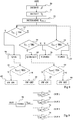
- the figure 1 illustrates a circuit for detecting the state of a load and two switches that control it according to one embodiment.
- This circuit comprises a charge Q in series with two switches T and SW between two application terminals 1 and 2 of an alternating voltage Vac.
- the switch T is, for example, a triac controlled by a control signal CT of a programmer (not shown), for example that of a washing machine.
- CT control signal
- the switch SW may symbolize a door opening detection contact of the machine so as to interrupt the supply of the motor when the door is opened (opening of the second switch ).
- a resistance R Q of value greater than the impedance of the load Q, is in parallel with the load.
- a resistance R SW of high value is in parallel with the switch SW, the resistance R SW being lower than the resistance R Q.
- a window comparator 5 (EVAL) is placed between the terminals 1 and 3 of the triac T. It evaluates a current Iin taken at the point of interconnection between the load Q and the triac T and provides an output OUT which is, for example, at a high level when the current Iin is located in a current window and at a low level otherwise.
- EVAL window comparator 5
- the figure 2 is a block diagram illustrating the operation of a window comparator 5 which can be used in the circuit of the figure 1 .
- the figure 3 illustrates the operation of the window comparator of the figure 2 by showing examples of typical signal patterns.
- the window comparator 5 compares the input AC current Iin with a current window around the current zero defined by a current threshold Iref (current source 9).
- the current Iin is first rectified (block 12). This full wave rectification is performed with respect to a DC voltage Vcc, which avoids the presence of a negative voltage downstream. Then, the rectified current
- the figure 4 illustrates an exemplary embodiment of the window comparator circuit 5 of the figure 2 , placed between two input terminals 1 and 3.
- Two bipolar transistors PNP T1 and T2 are each connected between a terminal 3 'and the terminal 1 corresponding to the terminal for applying a DC voltage Vcc.
- the terminal 3 ' is connected to the input terminal 3 via a resistor Rin of voltage-current conversion.
- the resistor Rin is of high value and its role is to ensure the voltage resistance of the comparator 5 relative to the AC input voltage.
- the emitter of the transistor T1 is connected to the terminal 3 'while the emitter of the transistor T2 is connected to the terminal 1.
- the transistor T1 is diode mounted and current mirrored on a PNP transistor T3 whose emitter is connected to the terminal 3 '.
- the transistor T2 is diode and current mirror mounted on a PNP transistor T4 whose emitter is connected to the terminal 1 and whose the collector is connected to the collector of transistor T3.
- the bases of transistors T1 and T3 are connected to the collector of transistor T1 (terminal 1).
- the bases of transistors T2 and T4 are connected to the collector of transistor T2.
- Transistors T1 and T2 provide the full wave rectification function (12, figure 2 ).
- the current mirror of transistors T1 and T3 (respectively T2 and T4) performs the function of current divider 14 with a ratio k, k being fixed by the ratio between the emitter surfaces of transistors (k for transistors T1 and T2, 1 for transistors T3 and T4).
- a current mirror formed of two NPN-type transistors T5 and T6 is responsible for taking, from the source 9, a current proportional to that of the collector of the transistor T3 or T4, according to the alternation of the current Iin.
- the transistor T5 has its collector connected to its base and to the collectors of the transistors T3 and T4 and its emitter connected to the ground 18.
- the transistor T6 has its emitter connected to the ground and to its collector connected to the current source 9 by defining the output terminal OUT.
- the bases of the transistors T5 and T6 are connected together to the collectors of the transistors T3, T4 and T5.
- the transistor T6 mirrored on the transistor T5 performs the subtraction of the current in the transistor T3 or T4 by the constant current Iref of the source 9, which constitutes the comparison function 16.
- the output OUT is at the low level (all the current Iref is absorbed by the transistor T6). Otherwise, the current source 9 provides a non-zero level on the output OUT.
- the current source 9 is made for example by means of a resistor, a transistor arrangement known as the Widlar source or any other integrated power source.
- the value of the current Iref will be suitably chosen according to the desired current thresholds.
- the window comparator 5 of the figure 1 could be any other known window comparator operating according to the scheme of the figure 2 or similar to this one.
- FIGS. 5A, 5B, 6A, 6B, 7A and 7B illustrate the operation of the circuit of the figure 1 .
- the Figures 5A and 5B illustrate, respectively, the shape of the current Iin and of the output OUT as a function of the different possible states of the triac T.
- Figures 6A and 6B represent paces of these same signals as a function of the different possible states of the charge Q considering that the triac T is open, and the Figures 7A and 7B according to the different states of the switch SW considering that the triac T is open.
- TH- and TH + thresholds are represented symmetrically with respect to the current zero.
- Threshold values TH + and TH- will be chosen by making a compromise between low values which ensure the detection of all possible states of the circuit of the figure 1 and high values that allow good detectability of these different states.
- TH- and TH + thresholds may have different values. For simplicity, we assume a purely resistive load Q.
- the Figures 5A and 5B illustrate the variation of the current Iin and of the output OUT as a function of the state of the triac T, considering that the load Q functions correctly and that the switch SW is closed.
- the current Iin is an alternating current proportional to the supply voltage Vac (curve 30 in solid lines in Figure 5A ).
- the corresponding OUT output is illustrated in Figure 5B by a curve 32 in solid lines.
- the current Iin goes below the threshold TH +, which causes the high state of the output OUT.
- the current Iin goes below the TH- threshold, which causes the output OUT to go low.
- the same pattern occurs on the output OUT during the next alternation between times t 3 and t 4 .
- the current Iin has the appearance of the dashed curve 34 and output OUT the appearance of the dashed curve 36.
- the curve 34 follows the curve 30 and the curve 36 follows the curve 32.
- the curve 34 remains at zero and the output OUT is in the high state.
- the current Iin is zero, as illustrated in FIG. Figure 5A by a phantom curve 38 and the output OUT remains in the high state, as illustrated by the curve in phantom lines 40.
- T OUT the duration during which the output OUT is in the high state on an alternation.
- the Figures 6A and 6B illustrate the variations of the current Iin and the output OUT as a function of the states of the load Q considering that the triac T is open and that the switch SW is closed.
- the current Iin follows the curve 30 and the output OUT the curve 32 (solid lines) identical to those of Figures 5A and 5B .
- the current Iin follows a dashed curve 42 and the output OUT corresponding a dashed curve 44.
- the increase in the impedance between terminals 2 and 3 causes a decrease in current Iin.
- the curve of the current Iin intersects the thresholds TH + and TH- at times t 1 ', t 2 ', t 3 'and t 4 ' different from the instants t 1 , t 2 , t 3 and t 4 .
- T OUT3 t 4 '-t 3 ' greater than the duration T OUT1 .
- the value of the duration T OUT thus makes it possible to determine the state of the charge Q.
- FIGS. 7A and 7B illustrate the variations of the output OUT according to the states of the switch SW considering that the triac T is open and the load Q functions correctly.
- the resistor R SW is different from the resistor R Q , the instants t 1 ", t 2 ", t 3 “and t 4 " are also different from the instants t 1 ', t 2 ', t 3 'and t 4 '.
- a duration T QUT4 is obtained greater than the duration T OUT1 and shorter than the duration T QUT3 .
- One embodiment provides for combining the previously described properties to obtain the state of the load and switches in series with the load.
- thresholds of duration TH1, TH2, TH3 and TH4 which are compared with the duration T OUT are suitably defined.
- T OUT less than the period of the supply voltage Vac (triac not closed on two consecutive alternations).
- the TH1 threshold is set lower than the TH2 threshold
- the TH3 threshold is lower than the TH1 threshold
- the TH4 threshold lies between the TH1 and TH2 thresholds.
- the TH1 and TH2 thresholds make it possible to characterize the state of the charge Q and the triac T.
- the triac T When the duration T OUT is below the threshold TH1, the triac T is open and the charge Q functions correctly. When the duration T OUT is between the thresholds TH1 and TH2, the triac T is open and the load Q is faulty or disconnected. When the duration T OUT is greater at TH2, the triac is in diode mode.
- the thresholds TH3 and TH4 make it possible to characterize the state of the switch SW. When the duration T OUT is below the threshold TH3 or when it is between the thresholds TH1 and TH4, the switch SW is closed. When the duration T OUT is between the thresholds TH3 and TH1 or TH4 and TH2, the switch SW is open.
- the resistance R SW may have a value greater than the resistance R Q.
- a duration T OUT3 shorter than the duration T OUT4 is obtained , and the thresholds TH1, TH2, TH3 and TH4 will be adapted accordingly.
- the figure 8 is a flowchart illustrating a method of monitoring the state of a load and at least one switch in series with the load according to one embodiment.
- T DIODE diode mode
- the duration T OUT is compared with the threshold TH1 (block 57). If the duration T OUT is lower than the threshold TH1 (block 58), this means that the load Q is connected and operates correctly (Q OK). In the opposite case, the duration T OUT is compared with the threshold TH2 (block 59). If the duration T OUT is lower than the threshold TH2 (block 60), this means that the load Q is faulty or disconnected (Q DEFECT). In the opposite case, the triac T is in diode mode (block 56).
- the duration T OUT is compared with the threshold TH3 (block 61). If the duration T OUT is lower than the threshold TH3 (block 62), this means that the switch SW is closed (SW ON). In the opposite case (block 63), the switch SW is open (SW OFF).
- the duration T OUT is compared with the threshold TH4 (block 64). If the duration T OUT is lower than the threshold TH4 (block 65), it means that the switch SW is closed (SW ON). In the opposite case (block 66), the switch SW is open (SW OFF).
- the method described above thus makes it possible to determine the state of all the elements constituting the circuit of the figure 1 .
- the steps for comparing the duration T OUT with the thresholds TH1, TH2, TH3 and TH4 can be carried out by various means, for example using a microprocessor. As a variant, these comparisons can be made using a time counter connected to the output OUT whose output is incremented when the output OUT is in the high state, and means for comparing the output level of this output. time comparator at thresholds.
- the figure 9 represents an embodiment of a system exploiting the signal provided by the circuit of the figure 1 .
- the output OUT of the circuit of the figure 1 is connected to the input of a counter 70 (TIMER) whose output V OUT is incremented when the output OUT is in the high state.
- the output V OUT is connected to four comparators 71 to 74 (C1 to C4), the second input of these comparators being fixed at voltage thresholds V TH1 , V TH2 , V TH3 and V TH4 which are determined according to the counter incrementation speed to match TH1, TH2, TH3 and TH4 thresholds.
- the state of the outputs OUT1, OUT2, OUT3 and OUT4 of the comparators 71 to 74 makes it possible to determine the state of the circuit of the figure 1 , in relation to the process of figure 8 .
- the thresholds TH1, TH2, TH3 and TH4 can be respectively fixed at 3 ms, 6 ms, 1 ms and 4 ms.
- the triac T is controlled in opening by the control signal CT, it is verified (study of the signal OUT) that it does not remain closed nor in diode mode. If the triac responds well to the command opening, we study the pace of the signal OUT to verify that the load Q is working properly and that the switch SW is closed.
- the triac T is commanded to close, it is checked that it does not present a fault by monitoring that the signal OUT is permanently in the high state.
- the resistance Rin of the window comparator circuit 5 of the figure 1 may be an external resistance and the other elements of the circuit 5, and the triac T, may be integrated in the same circuit.
- FIGS. 10A to 10G are timing diagrams illustrating a method of monitoring the state of a load according to another embodiment.
- the switch T can be a triac.
- a resistance R Q is placed in parallel with the charge Q and a window comparator, which measures a current Iin taken at the point of interconnection between the load Q and the switch T, is placed in parallel with the switch T.
- the figure 10A is a timing diagram illustrating the shape of the current Iin in two cases where the switch T is open and the state of the charge Q varies.
- Curve 80 illustrates the case where the load Q is working properly and curve 82 illustrates the case where the load Q is faulty or disconnected.
- the method according to one embodiment is to detect the value of the signal on the output OUT of the window comparator at selected times, which allows to know the state of the switch T and the load Q.
- the figure 10B is a chronogram on which are illustrated such instants ⁇ 1, ⁇ 2, ⁇ 3 and ⁇ 4.
- the instant ⁇ 1 corresponds to the maximum of the AC supply voltage (Vac) and the instant ⁇ 3 corresponds to the minimum of this voltage.
- the instant ⁇ 2 is between the instant ⁇ 1 and the end of the positive alternation of the AC voltage and the instant ⁇ 4 is between the instant ⁇ 3 and the end of the negative alternation of the AC voltage.
- the instants ⁇ 2 and ⁇ 4 are chosen so that the signal on the output OUT is, at these times, in a state when the load Q is operating correctly and in another state when the load Q is connected and faulty or disconnected.
- the chronograms of Figures 10C to 10G illustrate the appearance of the signal on the output OUT in several states of the circuit.
- the Figure 10C illustrates the signal 84 on the output OUT when the triac T is open and the load Q is working properly.
- the figure 10D Figure 86 shows the OUT signal when the triac T is in diode mode and the load Q is working properly.
- the figure 10E illustrates the appearance of the signal OUT 88 when the triac T is open and the charge Q has a fault or is disconnected.
- the figure 10F illustrates the pace 90 of the signal OUT when the triac T is in diode mode and the load Q has a failure or is disconnected.
- the figure 10G illustrates the pace 92 of the signal OUT when the triac is closed.
- the state of the signal is stored on the output OUT at times ⁇ 1, ⁇ 2, ⁇ 3 and ⁇ 4 (high state, 1, or low, 0). Then, we compare, by logical state words, these states to the following table which links the different possible states of the charge Q and the triac T with the corresponding levels of the output OUT at times ⁇ 1, ⁇ 2, ⁇ 3 and ⁇ 4.
- the control signal CT of the switch T (level 1 if the switch is controlled in closing and level 0 if the switch is controlled in opening) is taken into account.
- the state of the switch T and the load Q is thus obtained as a function of the control signal CT.
- This detection method can also make it possible to detect the state of all the elements of a circuit such as that of the figure 1 further comprising a switch SW. For that, it is enough to fix additional instants during which one detects the state of the signal on the output OUT.
- the circuit of the figure 1 at least 8 instants of detection adapted to obtain the state of all elements of the circuit (load Q, switches T and SW).
- the figure 11 illustrates a circuit for monitoring the state of two charges in parallel according to another embodiment.
- This circuit comprises two branches in parallel placed between two terminals 1 and 2 'for applying an AC supply voltage Vac.
- the first branch comprises, in series, a load Q and a triac T controlled by a control signal CT of a programmer (not shown).
- a resistor R Q greater than the impedance of the load Q, is placed in parallel with the load Q.
- the second branch comprises a load Q2 in series with a triac Tr2 controlled by a control signal CT2 of a programmer (not shown)
- a resistor R Q2 greater than the impedance of the load Q2, is placed in parallel with the load Q2.
- a 5 'window comparator (EVAL) of the same type as that shown in FIG.
- Figures 2 and 4 (except that the resistor Rin is external in the case of the comparator 5 '), is placed between the terminal 1 and a terminal 4.
- the terminal 4 is connected to the point of interconnection between the triac T and the load Q via a resistor Rin of voltage-current conversion, the current flowing in this resistor being called Iin.
- Terminal 4 is also connected to the interconnection point of triac Tr2 and charge Q2 via a resistor Rin 2 of voltage-current conversion, the current flowing in this resistor being called Iin 2 .
- the resistors Rin and Rin 2 have high values and their role is to ensure the voltage resistance of the window comparator 5 'with respect to the AC input voltage Vac.
- the comparator evaluates the sum Iin 'of the currents Iin and Iin 2 and provides an output OUT which is, for example, at a high level when the current Iin' is located in a current window and at a low level otherwise. This current window will be adapted to the desired selection.
- this circuit operates in much the same way as the circuit represented in FIG. figure 1 .
- the different values of resistors Rin, Rin 2, R Q and R Q2 are used to temporally shift the switching instants of the signal on the OUT output when there is change in the state of the circuit.
- the current Iin varies, which has repercussions on the current Iin 'and therefore on the switching times of the signal on the output OUT.
- the triac Tr2 is open and an element of the second branch is faulty, the current Iin 2 varies and the switching times of the signal on the output OUT also.
- the invention applies regardless of the type of load that is to be monitored, provided that it has, in normal operation, a relatively low impedance compared to the resistance with which it is in parallel.
- the process described here can be used in household and similar electrical appliances, for example an instantaneous water heater, a motor compressor, a refrigeration appliance, an ice cream maker or an ice-producing appliance, a heat pump electric, an air conditioner, a dehumidifier, for example to meet the standard IEC / EN 60335-1.
Landscapes
- Engineering & Computer Science (AREA)
- Physics & Mathematics (AREA)
- General Physics & Mathematics (AREA)
- Power Engineering (AREA)
- General Engineering & Computer Science (AREA)
- Multimedia (AREA)
- Electronic Switches (AREA)
- Measurement Of Current Or Voltage (AREA)
Claims (9)
- Ein Verfahren zum Detektieren des Zustands von wenigstens einem Element einer Schaltung, die Folgendes aufweist eine oder mehrere Lasten (Q), die durch eine Wechselspannung (Vac) und in Reihe mit wenigstens einem ersten Schalter (T) mit Leistung versorgt werden, dadurch gekennzeichnet, dass der Zustand des Elements durch Analysieren erhalten wird, und zwar zu verschiedenen Zeitpunkten (σ1, σ2, σ3, σ4) in einer Periode der Wechselspannung, wobei die Amplitude eines Stroms (Iin) von dem Knotenpunkt der Last und des ersten Schalters abgetastet wird, wobei die Analyse folgendes beinhaltet Vergleichen zu jedem Zeitpunkt (σ1, σ2, σ3, σ4) der Amplitude des Stroms (Iin) mit wenigstens einem Stromschwellenwert (TH-; TH+), Bilden eines Wortes von logischen Zuständen aus dem Ergebnis des Vergleichs und Vergleichen dieses logischen Zustandswortes mit in einer Tabelle gespeicherten Wörtern.
- Verfahren nach Anspruch 1, wobei ein erster Zeitpunkt (σ1) mit dem Maximum der Wechselspannung (Vac) korrespondiert, ein zweiter Zeitpunkt (σ3) mit dem Wechselspannungsminimum korrespondiert, ein dritter Zeitpunkt (σ2) zwischen dem ersten Zeitpunkt und dem Ende der positiven Halbwelle der Wechselspannung liegt, und ein vierter Zeitpunkt (σ4) zwischen dem zweiten Zeitpunkt und dem Ende der negativen Halbwelle der Wechselspannung liegt.
- Verfahren nach Anspruch 1 oder 2, wobei ein erster Stromschwellenwert (TH+) während der positiven Halbwelle der Wechselspannung (Vac) definiert ist und ein zweiter Stromschwellenwert (TH-) während der negativen Halbwelle der Wechselspannung definiert ist.
- Verfahren nach einem der vorhergehenden Ansprüche, das ferner das Bestimmen des Zustands eines zweiten Schalters (SW) ermöglicht, der in Reihe mit dem ersten Schalter (T) und der Last (Q) angeordnet ist durch Analysieren der Amplitude des Stroms (Iin), die von dem Knotenpunkt der Last und von dem ersten Schalter abgetastet wird, wenigstens acht Mal pro Periode der Wechselspannung (Vac).
- Verfahren nach einem der vorhergehenden Ansprüche, das ferner das Bestimmen des Zustands von wenigstens einem Element eines wenigstens zweiten Zweiges ermöglicht, der parallel zu einem ersten Zweig ist, der in Reihe wenigstens die Last (Q) und wenigstens den ersten Schalter (T) aufweist, wobei der zweite Zweig wenigstens eine zweite Last (Q2) und wenigstens einen dritten Schalter (Tr2) aufweist durch Analysieren zu mehreren Zeitpunkten in einer Periode der Wechselspannung (Vac) der Amplitude eines Stroms (Iin'), der gleich ist zu der Summe des Stroms (Iin), der von dem Knotenpunkt der ersten Last (Q) und des ersten Schalters und von einem Strom (Iin2), der von dem Knotenpunkt der zweiten Last (Q2) und des dritten Schalters (Tr2) abgetastet wird,.
- Verfahren nach einem der Ansprüche 1 bis 5, angewandt auf das Beobachten eines elektrischen Haushaltsgerätes gemäß dem IEC/EN 60335-1 Standard.
- Eine Schaltung zum Detektieren des Zustands von wenigstens einem Element einer Schaltung mit einem oder mehreren Lasten (Q), die durch eine Wechselspannung (Vac) in Reihe mit wenigstens einem ersten Schalter (T) mit Leistung versorgt wird, dadurch gekennzeichnet, dass sie Folgendes aufweist Mittel zum Analysieren der Amplitude eines Stroms (Iin), der von dem Knotenpunkt der Last und des ersten Schalters zu mehreren Zeitpunkten (σ1, σ2, σ3, σ4) in einer Periode der Wechselspannung abgetastet wird, zum Vergleichen der Amplitude des Stroms (Iin) mit wenigstens einem Stromschwellenwert (TH-; TH+) zu jedem Zeitpunkt zum Bilden eines Wortes von logischen Zuständen aus dem Ergebnis der Vergleiche und zum Vergleichen dieses logischen Zustandswortes mit in einer Tabelle gespeicherten Wörtern.
- Schaltung nach Anspruch 7, die ferner Folgendes aufweist wenigstens einen zweiten Schalter (SW) in Reihe mit der Last (Q) und dem ersten Schalter (T), dessen Zustand bestimmt werden kann durch die Mittel zum Analysieren der Amplitude des Stroms (Iin), der von dem Knotenpunkt der Last und des ersten Schalters wenigstens acht Mal pro Periode des Wechselstroms (Vac) abgetastet wird.
- Schaltung nach Anspruch 7 oder 8, die einen zweiten Zweig parallel mit einem ersten Zweig besitzt, der Folgendes aufweist wenigstens die Last (Q) und wenigstens den ersten Schalter (T), wobei der zweite Zweig wenigstens eine zweite Last (Q2) und einen dritten Schalter (T2) aufweist, wobei dessen Zustände bestimmt werden können durch die Mittel zum Analysieren der Amplitude eines Stroms (Iin'), der gleich der Summe des Stroms (Iin) ist, der von dem Knotenpunkt der ersten Last (Q) und dem ersten Schalter (T) und des Stroms (Iin2), der von dem Knotenpunkt der zweiten Last (Q2) und dem dritten Schalter (Tr2) abgetastet wird.
Applications Claiming Priority (1)
| Application Number | Priority Date | Filing Date | Title |
|---|---|---|---|
| FR0852085A FR2929408B1 (fr) | 2008-03-31 | 2008-03-31 | Detection de l'etat des elements d'une branche electrique comprenant une charge et un interrupteur |
Publications (2)
| Publication Number | Publication Date |
|---|---|
| EP2107382A1 EP2107382A1 (de) | 2009-10-07 |
| EP2107382B1 true EP2107382B1 (de) | 2018-10-31 |
Family
ID=39866533
Family Applications (1)
| Application Number | Title | Priority Date | Filing Date |
|---|---|---|---|
| EP09155771.0A Ceased EP2107382B1 (de) | 2008-03-31 | 2009-03-20 | Zustandserkennung der Elemente eines Zweigs einer Stromleitung, die eine Last und einen Schalter umfasst |
Country Status (4)
| Country | Link |
|---|---|
| US (1) | US8461845B2 (de) |
| EP (1) | EP2107382B1 (de) |
| KR (1) | KR101569858B1 (de) |
| FR (1) | FR2929408B1 (de) |
Families Citing this family (3)
| Publication number | Priority date | Publication date | Assignee | Title |
|---|---|---|---|---|
| DE102012218773A1 (de) * | 2012-10-15 | 2014-04-17 | Continental Automotive Gmbh | Verfahren und Einrichtung zur Messung eines Stroms durch einen Schalter |
| US9835687B2 (en) * | 2014-12-17 | 2017-12-05 | Nxp Usa, Inc. | System and method for switch status detection |
| US9897633B2 (en) * | 2014-12-17 | 2018-02-20 | Nxp Usa, Inc. | System and method for switch status detection |
Citations (3)
| Publication number | Priority date | Publication date | Assignee | Title |
|---|---|---|---|---|
| EP0843400A1 (de) * | 1996-11-18 | 1998-05-20 | Schneider Electric Sa | Einrichtung zur frühzeitigen Erkennen von Fehlern mit Lasttypidentifikation |
| US6710580B2 (en) * | 2000-12-14 | 2004-03-23 | Kokusan Denki Co., Ltd. | Method and apparatus for overload-controlling inverter power generation apparatus |
| EP1885059A2 (de) * | 2006-07-28 | 2008-02-06 | All Welding Technologies AG | Elektronenstrahlanlage zur Materialbearbeitung und Stromaddieranordnung zur schnellen Ansteuerung einer Induktivität und Bilderzeugungsvorrichtung für eine Elektronenstrahlanlage zur Materialbearbeitung |
Family Cites Families (21)
| Publication number | Priority date | Publication date | Assignee | Title |
|---|---|---|---|---|
| DE2602916A1 (de) * | 1976-01-27 | 1977-08-18 | Martin Dr Ing Mueller | Verfahren zur messung der linearen verzerrungsparameter und geraet zu dessen durchfuehrung (ii) |
| US4142493A (en) * | 1977-09-29 | 1979-03-06 | The Bendix Corporation | Closed loop exhaust gas recirculation control system |
| US4369403A (en) * | 1980-03-05 | 1983-01-18 | The Scott & Fetzer Company | Power factor controller for induction motor |
| CA1292770C (en) * | 1986-07-30 | 1991-12-03 | Kenneth Lipman | Apparatus and method for controlling a force commutated inverter |
| US4932246A (en) * | 1989-02-22 | 1990-06-12 | Motorola, Inc. | Diagnostic fault test system and circuit |
| US5173867A (en) * | 1990-07-27 | 1992-12-22 | Bha Group, Inc. | Multiple rapper control for electrostatic precipitator |
| US5621627A (en) * | 1995-04-14 | 1997-04-15 | Ac International Inc. | A.C. to A.C. power converter for the adaptive correction of waveform abnormalities |
| DE19617054C2 (de) * | 1996-04-29 | 2002-05-08 | Semikron Elektronik Gmbh | Überstrom- und Kurzschlußsicherung |
| DE19723456C2 (de) * | 1997-06-04 | 2003-03-27 | Siemens Ag | Fehlschlußerkennungseinrichtung für elektrische Verbraucher |
| US7039821B1 (en) * | 1998-12-31 | 2006-05-02 | Potega Patrick H | Hardware for configuring and delivering power |
| US6724329B2 (en) * | 2002-04-24 | 2004-04-20 | Intel Corporation | Decision feedback equalization employing a lookup table |
| US20040003169A1 (en) * | 2002-06-27 | 2004-01-01 | Josh Meit | Method for executing look up table function |
| NL1021168C2 (nl) * | 2002-07-26 | 2004-01-27 | Spaarstekker B V | Schakeleenheid, elektrisch apparaat omvattende een dergelijke schakeleenheid, gebruik van een dergelijke schakeleenheid, en werkwijze voor het schakelen van een verbinding tussen een lichtnet en een belasting. |
| JP4670413B2 (ja) * | 2004-07-07 | 2011-04-13 | トヨタ自動車株式会社 | 電源装置 |
| FR2874700B1 (fr) * | 2004-08-31 | 2006-11-17 | St Microelectronics Sa | Detection de l'etat d'alimentation d'une charge alimentee par une tension variable |
| JP2007113829A (ja) * | 2005-10-20 | 2007-05-10 | Sharp Corp | 電源コード接続位置の表示構造および冷蔵庫 |
| TWI277897B (en) * | 2005-10-20 | 2007-04-01 | Via Tech Inc | Control module, and related control chip and identification method |
| JP4833775B2 (ja) * | 2006-09-06 | 2011-12-07 | 日本電産リード株式会社 | 振幅算出装置およびそれを備えるインピーダンス測定装置、ならびに振幅算出方法およびそれを備えるインピーダンス測定方法 |
| EP1863214A1 (de) * | 2007-01-25 | 2007-12-05 | Agilent Technologies, Inc. | Analyse von digitalen Signalen mit Auswertung ausgewählter Signalbits |
| US20090154042A1 (en) * | 2007-12-17 | 2009-06-18 | Satec Ltd. | Over current protection method and device |
| US20110133743A1 (en) * | 2010-04-30 | 2011-06-09 | Werner Barton | Fault detection device and method for detecting an electrical fault |
-
2008
- 2008-03-31 FR FR0852085A patent/FR2929408B1/fr not_active Expired - Fee Related
-
2009
- 2009-03-20 EP EP09155771.0A patent/EP2107382B1/de not_active Ceased
- 2009-03-23 US US12/383,324 patent/US8461845B2/en not_active Expired - Fee Related
- 2009-03-24 KR KR1020090025110A patent/KR101569858B1/ko not_active Expired - Fee Related
Patent Citations (3)
| Publication number | Priority date | Publication date | Assignee | Title |
|---|---|---|---|---|
| EP0843400A1 (de) * | 1996-11-18 | 1998-05-20 | Schneider Electric Sa | Einrichtung zur frühzeitigen Erkennen von Fehlern mit Lasttypidentifikation |
| US6710580B2 (en) * | 2000-12-14 | 2004-03-23 | Kokusan Denki Co., Ltd. | Method and apparatus for overload-controlling inverter power generation apparatus |
| EP1885059A2 (de) * | 2006-07-28 | 2008-02-06 | All Welding Technologies AG | Elektronenstrahlanlage zur Materialbearbeitung und Stromaddieranordnung zur schnellen Ansteuerung einer Induktivität und Bilderzeugungsvorrichtung für eine Elektronenstrahlanlage zur Materialbearbeitung |
Also Published As
| Publication number | Publication date |
|---|---|
| FR2929408A1 (fr) | 2009-10-02 |
| FR2929408B1 (fr) | 2010-04-09 |
| EP2107382A1 (de) | 2009-10-07 |
| KR20090104677A (ko) | 2009-10-06 |
| US8461845B2 (en) | 2013-06-11 |
| KR101569858B1 (ko) | 2015-11-17 |
| US20090261806A1 (en) | 2009-10-22 |
Similar Documents
| Publication | Publication Date | Title |
|---|---|---|
| EP0645626B1 (de) | Messvorrichtung für entfernbare Sensoren | |
| FR2680007A1 (fr) | Dispositif de controle d'un appareil electrique dans un vehicule et des elements d'excitation le commandant. | |
| FR2680585A1 (fr) | Circuit generateur de tension interne correspondant a une tension externe appliquee a une puce a semi-conducteur. | |
| FR2760163A1 (fr) | Appareil de telecommunication muni d'un dispositif de reconnaissance de peripheriques | |
| EP2107382B1 (de) | Zustandserkennung der Elemente eines Zweigs einer Stromleitung, die eine Last und einen Schalter umfasst | |
| WO2015124305A1 (fr) | Detection de circuit ouvert dans une structure de commutation | |
| CA2315896C (fr) | Circuit electronique de surveillance de tension electrique | |
| FR2875346A1 (fr) | Dispositif de commande de moteur | |
| EP1428081B1 (de) | Steuereinrichtung für die werkzeugabnutzung und/oder werkzeugausfall für ein maschinenwerkzeug | |
| FR2671190A1 (fr) | Pont de mesure de tension de reference pour dispositif de controle et de mesure de l'isolement d'un reseau electrique a tension continue. | |
| EP3103178B1 (de) | Verfahren und schaltung zur erfassung eines elektrischen lichtbogens in einer schaltung und schaltvorrichtung mit solch einer schaltung | |
| FR2923331B1 (fr) | Appareil electrique rotatif pour automobile | |
| FR2844625A1 (fr) | Procede de commande de l'activation d'un actionneur electromecanique | |
| FR2563956A1 (fr) | Circuit integrable pour l'echantillonnage de la tension d'une charge | |
| WO2019215400A1 (fr) | Procédé de détermination d'un courant estimé d'un moteur électrique triphasé en mode dégradé | |
| JP2001289897A (ja) | ワイヤーハーネス検査装置 | |
| EP0458678A1 (de) | Automatische Einrichtung für die Rauschmessung elektronischer Komponenten | |
| EP1420262B1 (de) | Verfahren und Vorrichtung zur Detektion mindestens eines Fehlers mindestens eines Schalters in einem elektronischen Umwandler | |
| JPH11258072A (ja) | センサ装置及びその運転方法 | |
| WO2013045800A1 (fr) | Circuit electrique, notamment pour distinguer la phase et le neutre d'un signal monophase | |
| EP1414147B1 (de) | Messverfahren für die von einem Motor abgegebene Leistung | |
| EP2037287A1 (de) | Verfahren zur Erkennung einer Störung in einem Einspeisungssystem von elektrischer Ladung | |
| JP2561076Y2 (ja) | 抵抗測定装置 | |
| FR3117670A1 (fr) | Composant électronique de détection d’une défaillance d’au moins un interrupteur d’un redresseur pour véhicule | |
| FR2702842A1 (fr) | Système de contrôle permanent de la conduction élecrique d'un réseau alternatif. |
Legal Events
| Date | Code | Title | Description |
|---|---|---|---|
| PUAI | Public reference made under article 153(3) epc to a published international application that has entered the european phase |
Free format text: ORIGINAL CODE: 0009012 |
|
| AK | Designated contracting states |
Kind code of ref document: A1 Designated state(s): AT BE BG CH CY CZ DE DK EE ES FI FR GB GR HR HU IE IS IT LI LT LU LV MC MK MT NL NO PL PT RO SE SI SK TR |
|
| AX | Request for extension of the european patent |
Extension state: AL BA RS |
|
| 17P | Request for examination filed |
Effective date: 20100309 |
|
| AKX | Designation fees paid |
Designated state(s): DE FR GB IT |
|
| 17Q | First examination report despatched |
Effective date: 20150824 |
|
| STAA | Information on the status of an ep patent application or granted ep patent |
Free format text: STATUS: EXAMINATION IS IN PROGRESS |
|
| GRAP | Despatch of communication of intention to grant a patent |
Free format text: ORIGINAL CODE: EPIDOSNIGR1 |
|
| STAA | Information on the status of an ep patent application or granted ep patent |
Free format text: STATUS: GRANT OF PATENT IS INTENDED |
|
| RIC1 | Information provided on ipc code assigned before grant |
Ipc: H02J 13/00 20060101ALI20180531BHEP Ipc: G01R 19/165 20060101AFI20180531BHEP Ipc: G01R 31/28 20060101ALI20180531BHEP Ipc: H01H 9/16 20060101ALI20180531BHEP |
|
| INTG | Intention to grant announced |
Effective date: 20180622 |
|
| RIN1 | Information on inventor provided before grant (corrected) |
Inventor name: PAILLET, PASCAL Inventor name: BENABDELAZIZ, GHAFOUR |
|
| GRAJ | Information related to disapproval of communication of intention to grant by the applicant or resumption of examination proceedings by the epo deleted |
Free format text: ORIGINAL CODE: EPIDOSDIGR1 |
|
| STAA | Information on the status of an ep patent application or granted ep patent |
Free format text: STATUS: EXAMINATION IS IN PROGRESS |
|
| GRAR | Information related to intention to grant a patent recorded |
Free format text: ORIGINAL CODE: EPIDOSNIGR71 |
|
| GRAS | Grant fee paid |
Free format text: ORIGINAL CODE: EPIDOSNIGR3 |
|
| STAA | Information on the status of an ep patent application or granted ep patent |
Free format text: STATUS: GRANT OF PATENT IS INTENDED |
|
| GRAA | (expected) grant |
Free format text: ORIGINAL CODE: 0009210 |
|
| STAA | Information on the status of an ep patent application or granted ep patent |
Free format text: STATUS: THE PATENT HAS BEEN GRANTED |
|
| INTC | Intention to grant announced (deleted) | ||
| INTG | Intention to grant announced |
Effective date: 20180920 |
|
| AK | Designated contracting states |
Kind code of ref document: B1 Designated state(s): DE FR GB IT |
|
| REG | Reference to a national code |
Ref country code: GB Ref legal event code: FG4D Free format text: NOT ENGLISH |
|
| REG | Reference to a national code |
Ref country code: DE Ref legal event code: R096 Ref document number: 602009055329 Country of ref document: DE |
|
| PG25 | Lapsed in a contracting state [announced via postgrant information from national office to epo] |
Ref country code: IT Free format text: LAPSE BECAUSE OF FAILURE TO SUBMIT A TRANSLATION OF THE DESCRIPTION OR TO PAY THE FEE WITHIN THE PRESCRIBED TIME-LIMIT Effective date: 20181031 |
|
| REG | Reference to a national code |
Ref country code: DE Ref legal event code: R097 Ref document number: 602009055329 Country of ref document: DE |
|
| PLBE | No opposition filed within time limit |
Free format text: ORIGINAL CODE: 0009261 |
|
| STAA | Information on the status of an ep patent application or granted ep patent |
Free format text: STATUS: NO OPPOSITION FILED WITHIN TIME LIMIT |
|
| 26N | No opposition filed |
Effective date: 20190801 |
|
| GBPC | Gb: european patent ceased through non-payment of renewal fee |
Effective date: 20190320 |
|
| PG25 | Lapsed in a contracting state [announced via postgrant information from national office to epo] |
Ref country code: GB Free format text: LAPSE BECAUSE OF NON-PAYMENT OF DUE FEES Effective date: 20190320 |
|
| PG25 | Lapsed in a contracting state [announced via postgrant information from national office to epo] |
Ref country code: FR Free format text: LAPSE BECAUSE OF NON-PAYMENT OF DUE FEES Effective date: 20190331 |
|
| PGFP | Annual fee paid to national office [announced via postgrant information from national office to epo] |
Ref country code: DE Payment date: 20230221 Year of fee payment: 15 |
|
| REG | Reference to a national code |
Ref country code: DE Ref legal event code: R119 Ref document number: 602009055329 Country of ref document: DE |
|
| PG25 | Lapsed in a contracting state [announced via postgrant information from national office to epo] |
Ref country code: DE Free format text: LAPSE BECAUSE OF NON-PAYMENT OF DUE FEES Effective date: 20241001 |
|
| PG25 | Lapsed in a contracting state [announced via postgrant information from national office to epo] |
Ref country code: DE Free format text: LAPSE BECAUSE OF NON-PAYMENT OF DUE FEES Effective date: 20241001 |