EP2107538A2 - Resonanzetikett - Google Patents
Resonanzetikett Download PDFInfo
- Publication number
- EP2107538A2 EP2107538A2 EP08252813A EP08252813A EP2107538A2 EP 2107538 A2 EP2107538 A2 EP 2107538A2 EP 08252813 A EP08252813 A EP 08252813A EP 08252813 A EP08252813 A EP 08252813A EP 2107538 A2 EP2107538 A2 EP 2107538A2
- Authority
- EP
- European Patent Office
- Prior art keywords
- electrode pattern
- resonance tag
- circuit layer
- layer
- wiring
- Prior art date
- Legal status (The legal status is an assumption and is not a legal conclusion. Google has not performed a legal analysis and makes no representation as to the accuracy of the status listed.)
- Granted
Links
Images


Classifications
-
- G—PHYSICS
- G08—SIGNALLING
- G08B—SIGNALLING SYSTEMS, e.g. PERSONAL CALLING SYSTEMS; ORDER TELEGRAPHS; ALARM SYSTEMS
- G08B13/00—Burglar, theft or intruder alarms
- G08B13/22—Electrical actuation
- G08B13/24—Electrical actuation by interference with electromagnetic field distribution
- G08B13/2402—Electronic Article Surveillance [EAS], i.e. systems using tags for detecting removal of a tagged item from a secure area, e.g. tags for detecting shoplifting
- G08B13/2428—Tag details
- G08B13/2437—Tag layered structure, processes for making layered tags
-
- G—PHYSICS
- G08—SIGNALLING
- G08B—SIGNALLING SYSTEMS, e.g. PERSONAL CALLING SYSTEMS; ORDER TELEGRAPHS; ALARM SYSTEMS
- G08B13/00—Burglar, theft or intruder alarms
- G08B13/22—Electrical actuation
- G08B13/24—Electrical actuation by interference with electromagnetic field distribution
- G08B13/2402—Electronic Article Surveillance [EAS], i.e. systems using tags for detecting removal of a tagged item from a secure area, e.g. tags for detecting shoplifting
- G08B13/2405—Electronic Article Surveillance [EAS], i.e. systems using tags for detecting removal of a tagged item from a secure area, e.g. tags for detecting shoplifting characterised by the tag technology used
- G08B13/2414—Electronic Article Surveillance [EAS], i.e. systems using tags for detecting removal of a tagged item from a secure area, e.g. tags for detecting shoplifting characterised by the tag technology used using inductive tags
- G08B13/242—Tag deactivation
Definitions
- the present invention generally relates to a resonance tag and, more particularly, to a revival preventing resonance tag.
- a conventional resonance tag is composed of a capacitor and a coil, and constituting a LC circuit.
- the resonance tags are attached to products at stores, libraries, etc., for preventing shoplifting.
- the resonance tag receives an electromagnetic wave from the detector, thereby causing the tag to resonate to reflect an electromagnetic wave with the same frequency. That allows detecting shoplifting.
- the resonance function of the tag is inactivated by a tag inactivator installed for example on a register.
- the resonance tag does not reflect electromagnetic wave, so that a product can pass the detector without alarm.
- the resonance tag is inactivated by appling a high voltage generated when the resonance tag is given a pulse wave or Joule heat accompanied by the high voltage to a dielectric layer of the capacitor to cause the dielectric breakdown thereof, thereby short-circuiting the LC circuit.
- the tag may be reactivated with two electrode patterns of the capacitor being insulated from each other again. As a result, there will be some troubles, and the resonance tags with preventing reactivation are needed.
- One object of the invention is to supply a reliable resonance tag, which can prevent reactivation and can be easily manufactured.
- a resonance tag includes a dielectric layer, a first circuit layer, a second circuit layer and a hard pad.
- the first circuit layer is formed on one surface of the dielectric layer, and the first circuit layer has a first electrode pattern and a coil.
- a second circuit layer is formed on the other surface of the dielectric layer, and the second circuit layer has a second electrode pattern and a wiring, the wiring.
- a hard pad is formed on the second circuit layer and corresponding to the wiring of the second circuit layer, and then an edge of the hard pad is beyond the edge of the wiring.
- the resonance tag After bent repeatedly, the resonance tag is cut into a permanent open-circuit solely by the hard pad. Therefore, an advantage of the resonance tag is more reliable and more easily manufactured compared with the conventional resonance tag.
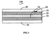
- FIG 1 is a schematic, side view showing a resonance tag according to the present invention.
- FIG 2 is a schematic, top view showing a first circuit layer of the present invention.
- FIG 3 is a schematic, top view showing a second circuit layer of the present resonance tag.
- FIG 4 is a schematic, top view showing a hard pad of the present resonance tag.
- FIG 5 is a schematic, side view showing the hard pad of FIG 4 .
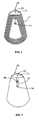
- FIG 6 is a schematic diagram showing the resonance tag attached to a shoe.
- the resonance tag 100 has a multi-layer structure that includes a first circuit layer 10, a dielectric layer 20 and a second circuit layer 30.
- the first circuit layer 10 is formed on one surface of the dielectric layer 20, and the second circuit layer 30 is formed on the other surface thereof.
- the resonance tag 100 can further include a cover layer 40 and a substrate layer 50, which are respectively attached to surfaces of the first circuit layer 10 and the second circuit layer 30 by adhesive layers (not labeled).
- the first circuit layer 10 and the second circuit layer 30 are thin film structures and made of any conductive material, such as, aluminum.
- the first circuit layer 10 includes a first electrode pattern 11 and a coil 12, and the second circuit layer 30 includes a second electrode pattern 31 and a wiring 32.
- the first electrode pattern 11 and the second electrode pattern 31 are opposite to each other, and therefore constitute a capacitor.
- the first electrode pattern 11 and the second electrode pattern 31 are corresponding to an upper-part electrode and a lower-part electrode of the capacitor.
- At least one groove is formed on one electrode of the capacitor.
- a first groove 13 and a second groove 33 are respectively formed on the first electrode pattern 11 and the second electrode pattern 31.
- the first groove 13 is facing and corresponding to the second groove 33.
- the coil 12 has one end electrically connected to the first electrode pattern 11, and the other end to a first connecting portion 14.
- one end of the wiring 32 is electrically connected to the second electrode pattern 31 and the other end thereof to a second connecting portion 34.
- the first connecting portion 14 and the second connecting portion 34 are conductive by a conductive tunnel 70 through the dielectric layer 20, as shown in FIG 1 .
- the first electrode pattern 11, the coil 12, the second electrode pattern 31 and the wiring 32 are electrically connected into a LC circuit.
- the capacitance C is given by a distance between two electron patterns of the capacitor.
- the distance between the first electrode pattern 11 and the second electrode pattern 31 i.e., a thickness of the dielectric layer
- the corresponding resonance frequency is about 8.2 MHz.
- the resonance tag 100 further includes a hard pad 80, which can been arranged on a surface of the second circuit layer 30 or sandwiched between the second circuit layer 30 and the substrate layer 50.
- the hard pad 80 is corresponding to the wiring 32. That is to say, an edge of the hard pad 80 is beyond that of the wiring 32.
- the wiring 32 may have a narrow portion, for a small size hard pad 80 supplied.
- a thickness of the hard pad 80 is in an approximate range of 0.6-1.5 ⁇ m.
- the hard pad 80 can be made of any suitable materials, such as steel.
- the hard pad 80 can be in any suitable shape, for instance, a circular shape with a hackle edge in a diameter about 4-8 millimeters (mm), a quadrate shape with a length of about 4-8 mm, a quadrate ring with the length of about 2-6 mm, a triangle shape and the like.
- the resonance tag 100 of the present invention is attached to a shoe 200 and on a middle part of soled thereof, which suffers more weight when being used.
- the electrode pattern of the resonance tag 100 is oriented toward heeled.
- the resonance tag 100 When the resonance tag 100 approaches a tag inactivator, the LC circuit thereof resonates with a pulse wave emitted from the tag inactivator, and then a high voltage is generated between the first electrode pattern 11 and the second electrode pattern 31. Thereafter, the dielectric layer 20 is broken down at a portion corresponding to the first and the second grooves 13, 33, the LC circuit is short-circuited and the resonance tag 100 is inactivated. As the inactivated resonance tag 100 is bent several times, the hard pad 80 will cut down the wiring 32, and thereby the LC circuit is an open-circuit. As a result, the reactivation of the resonant tag 100 is prevented.
Landscapes
- Physics & Mathematics (AREA)
- Engineering & Computer Science (AREA)
- Automation & Control Theory (AREA)
- Computer Security & Cryptography (AREA)
- Electromagnetism (AREA)
- General Physics & Mathematics (AREA)
- Burglar Alarm Systems (AREA)
- Parts Printed On Printed Circuit Boards (AREA)
- Production Of Multi-Layered Print Wiring Board (AREA)
Applications Claiming Priority (1)
| Application Number | Priority Date | Filing Date | Title |
|---|---|---|---|
| CN2008101033914A CN101551873B (zh) | 2008-04-03 | 2008-04-03 | 摩擦式防复活射频防盗标签 |
Publications (3)
| Publication Number | Publication Date |
|---|---|
| EP2107538A2 true EP2107538A2 (de) | 2009-10-07 |
| EP2107538A3 EP2107538A3 (de) | 2010-07-21 |
| EP2107538B1 EP2107538B1 (de) | 2011-11-23 |
Family
ID=40834322
Family Applications (1)
| Application Number | Title | Priority Date | Filing Date |
|---|---|---|---|
| EP08252813A Active EP2107538B1 (de) | 2008-04-03 | 2008-08-23 | Resonanzetikett |
Country Status (4)
| Country | Link |
|---|---|
| US (1) | US7782210B2 (de) |
| EP (1) | EP2107538B1 (de) |
| CN (1) | CN101551873B (de) |
| AT (1) | ATE534982T1 (de) |
Families Citing this family (2)
| Publication number | Priority date | Publication date | Assignee | Title |
|---|---|---|---|---|
| US8297519B2 (en) | 2010-08-06 | 2012-10-30 | Avery Dennison Corporation | Privacy protection packet for holding free floating security devices with deactivation assisted by perforations in the packet only |
| CN107845223A (zh) * | 2017-10-20 | 2018-03-27 | 宁波讯强电子科技有限公司 | 去激活后不可再次激活的声磁防盗标签及永久去激活方法 |
Family Cites Families (8)
| Publication number | Priority date | Publication date | Assignee | Title |
|---|---|---|---|---|
| US4498076A (en) * | 1982-05-10 | 1985-02-05 | Lichtblau G J | Resonant tag and deactivator for use in an electronic security system |
| US5012225A (en) * | 1989-12-15 | 1991-04-30 | Checkpoint Systems, Inc. | System for deactivating a field-sensitive tag or label |
| US5142270A (en) * | 1991-05-22 | 1992-08-25 | Checkpoint Systems Inc. | Stabilized resonant tag circuit and deactivator |
| US5574431A (en) * | 1995-08-29 | 1996-11-12 | Checkpoint Systems, Inc. | Deactivateable security tag |
| JP3266089B2 (ja) * | 1997-12-25 | 2002-03-18 | 三菱マテリアル株式会社 | 電波式盗難検出装置 |
| JP3436300B2 (ja) * | 1998-03-24 | 2003-08-11 | 三菱マテリアル株式会社 | 盗難防止用タグ及びその取付方法 |
| CN100487737C (zh) * | 2003-02-28 | 2009-05-13 | 上海埃塞电子有限公司 | 解码后不可复活的安全标签及其制造方法 |
| CN201025567Y (zh) * | 2007-03-06 | 2008-02-20 | 北京顺特科技有限公司 | 高灵敏度和防复活的防伪防盗标签 |
-
2008
- 2008-04-03 CN CN2008101033914A patent/CN101551873B/zh active Active
- 2008-08-06 US US12/186,531 patent/US7782210B2/en active Active
- 2008-08-23 EP EP08252813A patent/EP2107538B1/de active Active
- 2008-08-23 AT AT08252813T patent/ATE534982T1/de active
Also Published As
| Publication number | Publication date |
|---|---|
| ATE534982T1 (de) | 2011-12-15 |
| CN101551873B (zh) | 2013-07-10 |
| EP2107538B1 (de) | 2011-11-23 |
| US7782210B2 (en) | 2010-08-24 |
| CN101551873A (zh) | 2009-10-07 |
| US20090251320A1 (en) | 2009-10-08 |
| EP2107538A3 (de) | 2010-07-21 |
Similar Documents
| Publication | Publication Date | Title |
|---|---|---|
| KR100492042B1 (ko) | 보안태그및제조방법 | |
| JP4884477B2 (ja) | キャパシタストラップ | |
| US9299586B1 (en) | Process for manufacturing a combination anti-theft and tracking tag | |
| US20060087437A1 (en) | Identification band with regions having electro-magnetically detectable regions | |
| US4689636A (en) | Deactivatable resonant marker for use in RF electronic article surveillance system | |
| CN113039558A (zh) | 检测系统、以及读取器 | |
| US7782210B2 (en) | Resonance tag | |
| EP1618656B1 (de) | Lc resonanzschaltkreis mit verstärkungskomponente | |
| US8444057B2 (en) | Security labels with reinforced windows and methods of making the same | |
| CN104303217A (zh) | 可永久失效的安全标签 | |
| US11276286B2 (en) | Detectable folded coil | |
| US11544518B2 (en) | Deactivatable metal tag | |
| US12361809B2 (en) | Anti-theft and tracking tag and methods of manufacturing same | |
| JP2002157560A (ja) | 共振タグ | |
| US9870686B2 (en) | Radio frequency label for packaging security | |
| JPH1166446A (ja) | 共振タグおよびその製造方法 | |
| JP2010026732A (ja) | セキュリティタグ | |
| WO2019111710A1 (ja) | 部品管理用カード | |
| CN101068722A (zh) | 追踪具有金属部分的容器和容器盖的方法和系统、与具有金属部分的容器一起使用的标签及标定这种标签的方法 | |
| JP2004287970A (ja) | 共振タグ及びそのキャパシタンス調整方法 | |
| JP2008108003A (ja) | セキュリティタグ | |
| JPH08115478A (ja) | 共鳴センサー | |
| JP2006139617A (ja) | 共振機能付チューブフィルム及び共振機能付容器 |
Legal Events
| Date | Code | Title | Description |
|---|---|---|---|
| PUAI | Public reference made under article 153(3) epc to a published international application that has entered the european phase |
Free format text: ORIGINAL CODE: 0009012 |
|
| AK | Designated contracting states |
Kind code of ref document: A2 Designated state(s): AT BE BG CH CY CZ DE DK EE ES FI FR GB GR HR HU IE IS IT LI LT LU LV MC MT NL NO PL PT RO SE SI SK TR |
|
| AX | Request for extension of the european patent |
Extension state: AL BA MK RS |
|
| PUAL | Search report despatched |
Free format text: ORIGINAL CODE: 0009013 |
|
| AK | Designated contracting states |
Kind code of ref document: A3 Designated state(s): AT BE BG CH CY CZ DE DK EE ES FI FR GB GR HR HU IE IS IT LI LT LU LV MC MT NL NO PL PT RO SE SI SK TR |
|
| AX | Request for extension of the european patent |
Extension state: AL BA MK RS |
|
| 17P | Request for examination filed |
Effective date: 20100907 |
|
| 17Q | First examination report despatched |
Effective date: 20110210 |
|
| AKX | Designation fees paid |
Designated state(s): AT BE BG CH CY CZ DE DK EE ES FI FR GB GR HR HU IE IS IT LI LT LU LV MC MT NL NO PL PT RO SE SI SK TR |
|
| RIC1 | Information provided on ipc code assigned before grant |
Ipc: G08B 13/24 20060101AFI20110426BHEP |
|
| GRAP | Despatch of communication of intention to grant a patent |
Free format text: ORIGINAL CODE: EPIDOSNIGR1 |
|
| RIN1 | Information on inventor provided before grant (corrected) |
Inventor name: CHEN, JIN-KE |
|
| GRAS | Grant fee paid |
Free format text: ORIGINAL CODE: EPIDOSNIGR3 |
|
| GRAA | (expected) grant |
Free format text: ORIGINAL CODE: 0009210 |
|
| AK | Designated contracting states |
Kind code of ref document: B1 Designated state(s): AT BE BG CH CY CZ DE DK EE ES FI FR GB GR HR HU IE IS IT LI LT LU LV MC MT NL NO PL PT RO SE SI SK TR |
|
| REG | Reference to a national code |
Ref country code: GB Ref legal event code: FG4D |
|
| REG | Reference to a national code |
Ref country code: CH Ref legal event code: EP |
|
| REG | Reference to a national code |
Ref country code: IE Ref legal event code: FG4D |
|
| REG | Reference to a national code |
Ref country code: NL Ref legal event code: T3 |
|
| REG | Reference to a national code |
Ref country code: DE Ref legal event code: R096 Ref document number: 602008011534 Country of ref document: DE Effective date: 20120119 |
|
| LTIE | Lt: invalidation of european patent or patent extension |
Effective date: 20111123 |
|
| PG25 | Lapsed in a contracting state [announced via postgrant information from national office to epo] |
Ref country code: IS Free format text: LAPSE BECAUSE OF FAILURE TO SUBMIT A TRANSLATION OF THE DESCRIPTION OR TO PAY THE FEE WITHIN THE PRESCRIBED TIME-LIMIT Effective date: 20120323 Ref country code: NO Free format text: LAPSE BECAUSE OF FAILURE TO SUBMIT A TRANSLATION OF THE DESCRIPTION OR TO PAY THE FEE WITHIN THE PRESCRIBED TIME-LIMIT Effective date: 20120223 Ref country code: LT Free format text: LAPSE BECAUSE OF FAILURE TO SUBMIT A TRANSLATION OF THE DESCRIPTION OR TO PAY THE FEE WITHIN THE PRESCRIBED TIME-LIMIT Effective date: 20111123 |
|
| PG25 | Lapsed in a contracting state [announced via postgrant information from national office to epo] |
Ref country code: PT Free format text: LAPSE BECAUSE OF FAILURE TO SUBMIT A TRANSLATION OF THE DESCRIPTION OR TO PAY THE FEE WITHIN THE PRESCRIBED TIME-LIMIT Effective date: 20120323 Ref country code: HR Free format text: LAPSE BECAUSE OF FAILURE TO SUBMIT A TRANSLATION OF THE DESCRIPTION OR TO PAY THE FEE WITHIN THE PRESCRIBED TIME-LIMIT Effective date: 20111123 Ref country code: LV Free format text: LAPSE BECAUSE OF FAILURE TO SUBMIT A TRANSLATION OF THE DESCRIPTION OR TO PAY THE FEE WITHIN THE PRESCRIBED TIME-LIMIT Effective date: 20111123 Ref country code: SE Free format text: LAPSE BECAUSE OF FAILURE TO SUBMIT A TRANSLATION OF THE DESCRIPTION OR TO PAY THE FEE WITHIN THE PRESCRIBED TIME-LIMIT Effective date: 20111123 Ref country code: SI Free format text: LAPSE BECAUSE OF FAILURE TO SUBMIT A TRANSLATION OF THE DESCRIPTION OR TO PAY THE FEE WITHIN THE PRESCRIBED TIME-LIMIT Effective date: 20111123 Ref country code: GR Free format text: LAPSE BECAUSE OF FAILURE TO SUBMIT A TRANSLATION OF THE DESCRIPTION OR TO PAY THE FEE WITHIN THE PRESCRIBED TIME-LIMIT Effective date: 20120224 |
|
| PG25 | Lapsed in a contracting state [announced via postgrant information from national office to epo] |
Ref country code: CY Free format text: LAPSE BECAUSE OF FAILURE TO SUBMIT A TRANSLATION OF THE DESCRIPTION OR TO PAY THE FEE WITHIN THE PRESCRIBED TIME-LIMIT Effective date: 20111123 |
|
| PG25 | Lapsed in a contracting state [announced via postgrant information from national office to epo] |
Ref country code: EE Free format text: LAPSE BECAUSE OF FAILURE TO SUBMIT A TRANSLATION OF THE DESCRIPTION OR TO PAY THE FEE WITHIN THE PRESCRIBED TIME-LIMIT Effective date: 20111123 Ref country code: SK Free format text: LAPSE BECAUSE OF FAILURE TO SUBMIT A TRANSLATION OF THE DESCRIPTION OR TO PAY THE FEE WITHIN THE PRESCRIBED TIME-LIMIT Effective date: 20111123 Ref country code: BG Free format text: LAPSE BECAUSE OF FAILURE TO SUBMIT A TRANSLATION OF THE DESCRIPTION OR TO PAY THE FEE WITHIN THE PRESCRIBED TIME-LIMIT Effective date: 20120223 Ref country code: CZ Free format text: LAPSE BECAUSE OF FAILURE TO SUBMIT A TRANSLATION OF THE DESCRIPTION OR TO PAY THE FEE WITHIN THE PRESCRIBED TIME-LIMIT Effective date: 20111123 Ref country code: DK Free format text: LAPSE BECAUSE OF FAILURE TO SUBMIT A TRANSLATION OF THE DESCRIPTION OR TO PAY THE FEE WITHIN THE PRESCRIBED TIME-LIMIT Effective date: 20111123 |
|
| PG25 | Lapsed in a contracting state [announced via postgrant information from national office to epo] |
Ref country code: RO Free format text: LAPSE BECAUSE OF FAILURE TO SUBMIT A TRANSLATION OF THE DESCRIPTION OR TO PAY THE FEE WITHIN THE PRESCRIBED TIME-LIMIT Effective date: 20111123 Ref country code: PL Free format text: LAPSE BECAUSE OF FAILURE TO SUBMIT A TRANSLATION OF THE DESCRIPTION OR TO PAY THE FEE WITHIN THE PRESCRIBED TIME-LIMIT Effective date: 20111123 |
|
| REG | Reference to a national code |
Ref country code: AT Ref legal event code: MK05 Ref document number: 534982 Country of ref document: AT Kind code of ref document: T Effective date: 20111123 |
|
| PLBE | No opposition filed within time limit |
Free format text: ORIGINAL CODE: 0009261 |
|
| STAA | Information on the status of an ep patent application or granted ep patent |
Free format text: STATUS: NO OPPOSITION FILED WITHIN TIME LIMIT |
|
| 26N | No opposition filed |
Effective date: 20120824 |
|
| REG | Reference to a national code |
Ref country code: DE Ref legal event code: R097 Ref document number: 602008011534 Country of ref document: DE Effective date: 20120824 |
|
| PG25 | Lapsed in a contracting state [announced via postgrant information from national office to epo] |
Ref country code: AT Free format text: LAPSE BECAUSE OF FAILURE TO SUBMIT A TRANSLATION OF THE DESCRIPTION OR TO PAY THE FEE WITHIN THE PRESCRIBED TIME-LIMIT Effective date: 20111123 |
|
| REG | Reference to a national code |
Ref country code: CH Ref legal event code: PL |
|
| PG25 | Lapsed in a contracting state [announced via postgrant information from national office to epo] |
Ref country code: MC Free format text: LAPSE BECAUSE OF NON-PAYMENT OF DUE FEES Effective date: 20120831 |
|
| PG25 | Lapsed in a contracting state [announced via postgrant information from national office to epo] |
Ref country code: LI Free format text: LAPSE BECAUSE OF NON-PAYMENT OF DUE FEES Effective date: 20120831 Ref country code: ES Free format text: LAPSE BECAUSE OF FAILURE TO SUBMIT A TRANSLATION OF THE DESCRIPTION OR TO PAY THE FEE WITHIN THE PRESCRIBED TIME-LIMIT Effective date: 20120305 Ref country code: CH Free format text: LAPSE BECAUSE OF NON-PAYMENT OF DUE FEES Effective date: 20120831 |
|
| PG25 | Lapsed in a contracting state [announced via postgrant information from national office to epo] |
Ref country code: FI Free format text: LAPSE BECAUSE OF FAILURE TO SUBMIT A TRANSLATION OF THE DESCRIPTION OR TO PAY THE FEE WITHIN THE PRESCRIBED TIME-LIMIT Effective date: 20111123 |
|
| PG25 | Lapsed in a contracting state [announced via postgrant information from national office to epo] |
Ref country code: MT Free format text: LAPSE BECAUSE OF FAILURE TO SUBMIT A TRANSLATION OF THE DESCRIPTION OR TO PAY THE FEE WITHIN THE PRESCRIBED TIME-LIMIT Effective date: 20111123 |
|
| PG25 | Lapsed in a contracting state [announced via postgrant information from national office to epo] |
Ref country code: TR Free format text: LAPSE BECAUSE OF FAILURE TO SUBMIT A TRANSLATION OF THE DESCRIPTION OR TO PAY THE FEE WITHIN THE PRESCRIBED TIME-LIMIT Effective date: 20111123 |
|
| PG25 | Lapsed in a contracting state [announced via postgrant information from national office to epo] |
Ref country code: LU Free format text: LAPSE BECAUSE OF NON-PAYMENT OF DUE FEES Effective date: 20120823 |
|
| PG25 | Lapsed in a contracting state [announced via postgrant information from national office to epo] |
Ref country code: HU Free format text: LAPSE BECAUSE OF FAILURE TO SUBMIT A TRANSLATION OF THE DESCRIPTION OR TO PAY THE FEE WITHIN THE PRESCRIBED TIME-LIMIT Effective date: 20080823 |
|
| REG | Reference to a national code |
Ref country code: FR Ref legal event code: PLFP Year of fee payment: 9 |
|
| REG | Reference to a national code |
Ref country code: FR Ref legal event code: PLFP Year of fee payment: 10 |
|
| REG | Reference to a national code |
Ref country code: FR Ref legal event code: PLFP Year of fee payment: 11 |
|
| PGFP | Annual fee paid to national office [announced via postgrant information from national office to epo] |
Ref country code: IE Payment date: 20200625 Year of fee payment: 13 |
|
| PGFP | Annual fee paid to national office [announced via postgrant information from national office to epo] |
Ref country code: NL Payment date: 20200722 Year of fee payment: 13 |
|
| PGFP | Annual fee paid to national office [announced via postgrant information from national office to epo] |
Ref country code: DE Payment date: 20200831 Year of fee payment: 13 |
|
| PGFP | Annual fee paid to national office [announced via postgrant information from national office to epo] |
Ref country code: BE Payment date: 20200827 Year of fee payment: 13 |
|
| REG | Reference to a national code |
Ref country code: DE Ref legal event code: R082 Ref document number: 602008011534 Country of ref document: DE Representative=s name: BAUER WAGNER PELLENGAHR SROKA PATENT- & RECHTS, DE |
|
| REG | Reference to a national code |
Ref country code: DE Ref legal event code: R119 Ref document number: 602008011534 Country of ref document: DE |
|
| REG | Reference to a national code |
Ref country code: NL Ref legal event code: MM Effective date: 20210901 |
|
| REG | Reference to a national code |
Ref country code: BE Ref legal event code: MM Effective date: 20210831 |
|
| PG25 | Lapsed in a contracting state [announced via postgrant information from national office to epo] |
Ref country code: NL Free format text: LAPSE BECAUSE OF NON-PAYMENT OF DUE FEES Effective date: 20210901 |
|
| PG25 | Lapsed in a contracting state [announced via postgrant information from national office to epo] |
Ref country code: IE Free format text: LAPSE BECAUSE OF NON-PAYMENT OF DUE FEES Effective date: 20210823 Ref country code: DE Free format text: LAPSE BECAUSE OF NON-PAYMENT OF DUE FEES Effective date: 20220301 Ref country code: BE Free format text: LAPSE BECAUSE OF NON-PAYMENT OF DUE FEES Effective date: 20210831 |
|
| PGFP | Annual fee paid to national office [announced via postgrant information from national office to epo] |
Ref country code: GB Payment date: 20250625 Year of fee payment: 18 |
|
| PGFP | Annual fee paid to national office [announced via postgrant information from national office to epo] |
Ref country code: FR Payment date: 20250619 Year of fee payment: 18 |
|
| PGFP | Annual fee paid to national office [announced via postgrant information from national office to epo] |
Ref country code: IT Payment date: 20250829 Year of fee payment: 18 |