EP2107549A2 - Module d'affichage à cristaux liquides - Google Patents
Module d'affichage à cristaux liquides Download PDFInfo
- Publication number
- EP2107549A2 EP2107549A2 EP09250779A EP09250779A EP2107549A2 EP 2107549 A2 EP2107549 A2 EP 2107549A2 EP 09250779 A EP09250779 A EP 09250779A EP 09250779 A EP09250779 A EP 09250779A EP 2107549 A2 EP2107549 A2 EP 2107549A2
- Authority
- EP
- European Patent Office
- Prior art keywords
- liquid crystal
- switches
- crystal cells
- strips
- cells
- Prior art date
- Legal status (The legal status is an assumption and is not a legal conclusion. Google has not performed a legal analysis and makes no representation as to the accuracy of the status listed.)
- Withdrawn
Links
Images


Classifications
-
- G—PHYSICS
- G09—EDUCATION; CRYPTOGRAPHY; DISPLAY; ADVERTISING; SEALS
- G09G—ARRANGEMENTS OR CIRCUITS FOR CONTROL OF INDICATING DEVICES USING STATIC MEANS TO PRESENT VARIABLE INFORMATION
- G09G3/00—Control arrangements or circuits, of interest only in connection with visual indicators other than cathode-ray tubes
- G09G3/20—Control arrangements or circuits, of interest only in connection with visual indicators other than cathode-ray tubes for presentation of an assembly of a number of characters, e.g. a page, by composing the assembly by combination of individual elements arranged in a matrix no fixed position being assigned to or needed to be assigned to the individual characters or partial characters
- G09G3/34—Control arrangements or circuits, of interest only in connection with visual indicators other than cathode-ray tubes for presentation of an assembly of a number of characters, e.g. a page, by composing the assembly by combination of individual elements arranged in a matrix no fixed position being assigned to or needed to be assigned to the individual characters or partial characters by control of light from an independent source
- G09G3/36—Control arrangements or circuits, of interest only in connection with visual indicators other than cathode-ray tubes for presentation of an assembly of a number of characters, e.g. a page, by composing the assembly by combination of individual elements arranged in a matrix no fixed position being assigned to or needed to be assigned to the individual characters or partial characters by control of light from an independent source using liquid crystals
- G09G3/3611—Control of matrices with row and column drivers
- G09G3/3648—Control of matrices with row and column drivers using an active matrix
- G09G3/3655—Details of drivers for counter electrodes, e.g. common electrodes for pixel capacitors or supplementary storage capacitors
-
- G—PHYSICS
- G02—OPTICS
- G02F—OPTICAL DEVICES OR ARRANGEMENTS FOR THE CONTROL OF LIGHT BY MODIFICATION OF THE OPTICAL PROPERTIES OF THE MEDIA OF THE ELEMENTS INVOLVED THEREIN; NON-LINEAR OPTICS; FREQUENCY-CHANGING OF LIGHT; OPTICAL LOGIC ELEMENTS; OPTICAL ANALOGUE/DIGITAL CONVERTERS
- G02F1/00—Devices or arrangements for the control of the intensity, colour, phase, polarisation or direction of light arriving from an independent light source, e.g. switching, gating or modulating; Non-linear optics
- G02F1/01—Devices or arrangements for the control of the intensity, colour, phase, polarisation or direction of light arriving from an independent light source, e.g. switching, gating or modulating; Non-linear optics for the control of the intensity, phase, polarisation or colour
- G02F1/13—Devices or arrangements for the control of the intensity, colour, phase, polarisation or direction of light arriving from an independent light source, e.g. switching, gating or modulating; Non-linear optics for the control of the intensity, phase, polarisation or colour based on liquid crystals, e.g. single liquid crystal display cells
- G02F1/133—Constructional arrangements; Operation of liquid crystal cells; Circuit arrangements
- G02F1/136—Liquid crystal cells structurally associated with a semi-conducting layer or substrate, e.g. cells forming part of an integrated circuit
- G02F1/1362—Active matrix addressed cells
- G02F1/136286—Wiring, e.g. gate line, drain line
-
- G—PHYSICS
- G09—EDUCATION; CRYPTOGRAPHY; DISPLAY; ADVERTISING; SEALS
- G09G—ARRANGEMENTS OR CIRCUITS FOR CONTROL OF INDICATING DEVICES USING STATIC MEANS TO PRESENT VARIABLE INFORMATION
- G09G3/00—Control arrangements or circuits, of interest only in connection with visual indicators other than cathode-ray tubes
- G09G3/20—Control arrangements or circuits, of interest only in connection with visual indicators other than cathode-ray tubes for presentation of an assembly of a number of characters, e.g. a page, by composing the assembly by combination of individual elements arranged in a matrix no fixed position being assigned to or needed to be assigned to the individual characters or partial characters
- G09G3/34—Control arrangements or circuits, of interest only in connection with visual indicators other than cathode-ray tubes for presentation of an assembly of a number of characters, e.g. a page, by composing the assembly by combination of individual elements arranged in a matrix no fixed position being assigned to or needed to be assigned to the individual characters or partial characters by control of light from an independent source
- G09G3/36—Control arrangements or circuits, of interest only in connection with visual indicators other than cathode-ray tubes for presentation of an assembly of a number of characters, e.g. a page, by composing the assembly by combination of individual elements arranged in a matrix no fixed position being assigned to or needed to be assigned to the individual characters or partial characters by control of light from an independent source using liquid crystals
- G09G3/3611—Control of matrices with row and column drivers
- G09G3/3614—Control of polarity reversal in general
-
- G—PHYSICS
- G02—OPTICS
- G02F—OPTICAL DEVICES OR ARRANGEMENTS FOR THE CONTROL OF LIGHT BY MODIFICATION OF THE OPTICAL PROPERTIES OF THE MEDIA OF THE ELEMENTS INVOLVED THEREIN; NON-LINEAR OPTICS; FREQUENCY-CHANGING OF LIGHT; OPTICAL LOGIC ELEMENTS; OPTICAL ANALOGUE/DIGITAL CONVERTERS
- G02F1/00—Devices or arrangements for the control of the intensity, colour, phase, polarisation or direction of light arriving from an independent light source, e.g. switching, gating or modulating; Non-linear optics
- G02F1/01—Devices or arrangements for the control of the intensity, colour, phase, polarisation or direction of light arriving from an independent light source, e.g. switching, gating or modulating; Non-linear optics for the control of the intensity, phase, polarisation or colour
- G02F1/13—Devices or arrangements for the control of the intensity, colour, phase, polarisation or direction of light arriving from an independent light source, e.g. switching, gating or modulating; Non-linear optics for the control of the intensity, phase, polarisation or colour based on liquid crystals, e.g. single liquid crystal display cells
- G02F1/133—Constructional arrangements; Operation of liquid crystal cells; Circuit arrangements
- G02F1/1333—Constructional arrangements; Manufacturing methods
- G02F1/1343—Electrodes
- G02F1/134309—Electrodes characterised by their geometrical arrangement
- G02F1/134318—Electrodes characterised by their geometrical arrangement having a patterned common electrode
-
- G—PHYSICS
- G09—EDUCATION; CRYPTOGRAPHY; DISPLAY; ADVERTISING; SEALS
- G09G—ARRANGEMENTS OR CIRCUITS FOR CONTROL OF INDICATING DEVICES USING STATIC MEANS TO PRESENT VARIABLE INFORMATION
- G09G2300/00—Aspects of the constitution of display devices
- G09G2300/04—Structural and physical details of display devices
- G09G2300/0421—Structural details of the set of electrodes
- G09G2300/0426—Layout of electrodes and connections
-
- G—PHYSICS
- G09—EDUCATION; CRYPTOGRAPHY; DISPLAY; ADVERTISING; SEALS
- G09G—ARRANGEMENTS OR CIRCUITS FOR CONTROL OF INDICATING DEVICES USING STATIC MEANS TO PRESENT VARIABLE INFORMATION
- G09G2320/00—Control of display operating conditions
- G09G2320/02—Improving the quality of display appearance
- G09G2320/0209—Crosstalk reduction, i.e. to reduce direct or indirect influences of signals directed to a certain pixel of the displayed image on other pixels of said image, inclusive of influences affecting pixels in different frames or fields or sub-images which constitute a same image, e.g. left and right images of a stereoscopic display
-
- G—PHYSICS
- G09—EDUCATION; CRYPTOGRAPHY; DISPLAY; ADVERTISING; SEALS
- G09G—ARRANGEMENTS OR CIRCUITS FOR CONTROL OF INDICATING DEVICES USING STATIC MEANS TO PRESENT VARIABLE INFORMATION
- G09G2330/00—Aspects of power supply; Aspects of display protection and defect management
- G09G2330/02—Details of power systems and of start or stop of display operation
- G09G2330/021—Power management, e.g. power saving
Definitions
- the present invention relates to a liquid crystal display module and a method of driving the liquid crystal display of such a module so as to reduce the overall power consumption.
- Liquid crystal displays are well known using a two-dimensional array of liquid crystal cells in which the cells share a plurality of signal lines in one direction and are selectively enabled by gate lines in a perpendicular direction.
- Drive circuits are provided which use the gate lines to enable respective sets of liquid crystal cells.
- the signal lines are then used to provide video signal levels to the enabled cells to charge those cells to the level required to give those cells their desired brightness.
- Each image pixel would typically include three liquid crystal cells corresponding respectively to red, green and blue.
- the red, green and blue liquid crystal cells of a pixel are provided on the same gate line and, indeed, can be driven by the same video signal.
- the video signal is provided first to the red liquid crystal cell by means of its signal line, then to the green liquid crystal cell by means of its signal line and finally to the blue liquid crystal cell by means of its signal line.
- the liquid crystal cells are normally all connected (on an opposite side to switches operated by the gate lines) to a common line which usually takes the form of a plate (COM plate) across the entire area of the liquid crystal display.
- the potential on the common line is varied in steps as a square wave so that the required inversion of sub-pixels or pixels occurs.
- Various forms of inversion are known: 1F frame inversion where all of the liquid crystal cells of a frame have the same potential for each frame, but the potential is changed from frame to frame; 1H inversion where all of the liquid crystal cells of a horizontal line have the same potential, but are inverted from line to line and frame to frame; and dot inversion where adjacent liquid crystal cells have opposite potential and are also inverted from frame to frame.
- the present application recognises that alternating the potential on the COM plate consumes a relatively large amount of power due to the large capacitance of the COM plate. Also, the present application recognises that having all of the liquid crystal cells connected together on the same COM plate can result in noise in the displayed image.
- a liquid crystal display module including:
- liquid crystal display module including:
- each row may be arranged along and connected to a respective strip.
- a strip is provided for each row of liquid crystal cells and the capacitance which needs to be driven for each row is reduced to the capacitance of one strip.
- the strips When the strips are not driven with either a high or a low voltage (corresponding to the two predetermined voltages), they can be driven with a standby voltage preferably midway between the high and low voltages.
- the driver circuit is configured simultaneously to drive only the two strips to said one of two predetermined potentials at any one time.
- the rows may be arrange as adjacent pairs of rows where each pair of rows is arranged along and connected to a respective strip.
- each strip is actually wide enough for two adjacent rows of liquid crystal cells. Because of the alternating arrangement of the liquid crystal cells with respect to the gate lines, each strip will have a central gate line operating alternate liquid crystal cells of two adjacent rows. It will also have gate lines on either side of that strip operating alternate liquid crystal cells of only one row of liquid crystal cells on that side of the strip.
- the driver circuit is configured to drive only the respective strip to said one of two predetermined potentials at any one time.
- the driver circuit is configured simultaneously to drive only the strip to said one of two predetermined potentials.
- the other strips are driven to a different predetermined potential.
- this different predetermined potential is chosen so as to minimise the average potential change that the driving circuit is required to create on any strip at any one time.
- the predetermined potential will usually be at least approximately mid way between the two COM inversion potentials.
- the present invention is applicable to LCD (Liquid Crystal Display) modules such as are used in mobile telephone devices or digital cameras, for instance as illustrated respectively in Figures 1 and 2 .
- the present invention could be applied to any LCD, including those with LCD driving circuits formed on the display panel of the LCD module itself.
- respective LCD modules 6 and 8 are provided for displaying images as required.
- FIG. 3 illustrates an LCD module 10 which is suitable for use in mobile telephone devices and digital cameras and which embodies the present invention.
- the LCD module 10 includes at least one plate 12 made of glass (or any other suitable transparent material) against which a liquid crystal display 16 is formed in any known manner.
- a driving circuit 14 is also formed on the glass plate 12.
- An LCD driving circuit 14 is illustrated at a lower portion of the display module 10.
- a similar driving circuit could be provided at any portion of the glass plate 12 around the display area 16 or, indeed, in a distributed manner around the display area 16.
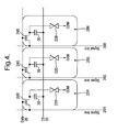
- Figure 4 illustrates one example of how the display area 16 can be implemented.
- the display area 16 is divided into a two-dimensional array of pixels.
- the pixels extend in horizontal rows in a first direction and in vertical columns in a second direction. By activating each pixel with a desired colour and brightness, an appropriate image can be displayed on the display 16.
- each pixel includes three pixel units 20R, 20G, 20B (otherwise known as sub-pixels) respectively for producing red, green and blue.
- Figure 4 illustrates the three pixel units 20R, 20G, 20B of a pixel arranged side by side in the first (horizontal) direction.
- the three pixel units 20R, 20G, 20B should be located close to one another in order to provide the desired visual combined colour, but the exact positioning of the pixel units is not critical.
- Each of the pixel units 20R, 20G, 20B includes a corresponding liquid crystal cell 22R, 22G, 22B.
- One side of every liquid crystal cell 22R, 22G, 22B is connected to a common line COM which, in the preferred embodiment, is formed as part of the glass plate 12 itself.
- the opposite side of each liquid crystal cell 22R, 22G, 22B is connected to a respective control transistor or switch 24R, 24G, 24B.
- all of the switches 24R, 24G, 24B in a row are controlled, in other words switched on or off, by means of a common gate line 26.
- a respective gate line is provided for each of the rows of the display 16.
- the inputs to the switches 24R, 24G, 24B are connected to signal lines 28R, 28G, 28B.
- all of the red pixel units 20R in the same column are connected to a single respective signal line 28R
- all of the green pixel units 20G in the same column are connected to a single respective signal line 28G
- all of the blue pixel units 20B in the same column are connected to a single respective signal line 28B.
- an image is provided row by row.
- a particular gate line 26 is driven to a voltage so as to turn on all of the switches or transistors 24R, 24G, 24B in its respective row. While that gate line enables that particular row or horizontal line, first all of the red signal lines 28R are used to drive all of the red liquid crystal cells 22R in that row, then all of the green signal lines 28G are used to drive all of the green LCD cells 22G in that particular row and, finally, all of the blue signal lines 28B are used to drive all of the blue liquid crystal cells 22B in that particular row.
- all of the pixel units 20R, 20G, 20B of a particular colour are driven simultaneously. However, other arrangements are also possible.
- the corresponding gate line 26 is driven to a voltage to turn off all of its corresponding switches or transistors 24R, 24G, 24B and another gate line is driven to a voltage to turn on its corresponding switches.
- Adjacent gate lines 26 can be driven one after the other, but other arrangements are possible. It will also be appreciated that different arrangements of arrays of pixel units can be provided to achieve the same effect.
- the liquid crystal capacitance is somewhat variable and it becomes difficult, with only the arrangement described above, to drive reliably the liquid crystal cells 22R, 22G, 22B to the appropriate or desired brightness levels.
- CS capacitors 30 are provided in parallel with the liquid crystal cells 22R, 22G, 22B. As illustrated, the CS capacitors 30 are provided between the signal driving end of the liquid crystal cells 22R, 22G, 22B and a CS line 32. For the arrangement described above, a CS line 32 is provided for each respective row or horizontal line. Thus, the CS capacitors 30 of all of the pixel units 20R, 20G, 20B of a respective row or horizontal line are connected to a corresponding respective CS line 32.
- the CS line 32 is driven with a voltage corresponding closely to the voltage of the common voltage COM. In this way, variations in the capacitance of the liquid crystal cells 22R, 22G, 22B have less effect on driving of those liquid crystal cells 22R, 22G, 22B.
- Figure 5 illustrates various signals for driving the first two horizontal lines of the display 16.
- inversion the polarity applied to the liquid crystal cells 22R, 22G, 22B each time they are used; this is known as inversion.
- the polarity is reversed.
- adjacent horizontal lines or rows are driven with opposite polarities.
- a vertical synchronous pulse having the length of one horizontal timing signifies a new frame. Also, a short horizontal synchronous pulse is provided to indicate each new horizontal line or row.
- Gate pulses are shown for the first and second horizontal lines. Each gate pulse lies within the horizontal line period and, during a gate pulse, the respective row or horizontal line of pixel units 20R, 20G, 20B are enabled in the manner described above. Thus, during the gate pulse for the first horizontal line, all of the switches/transistors 24R, 24G, 24B of the first horizontal line are enabled, but none others. Similarly, for the second horizontal gate pulse, only the switches/transistors of the second row or horizontal line are enabled.
- the voltages for a red pixel unit 20R, a green pixel unit 20G and a blue pixel unit 20B are indicated for first and second horizontal lines.
- the COM signal is illustrated as a dashed line overlying the voltage illustrated for the liquid crystal cells 22R, 22G, 22B of the pixel units 20R, 20G, 20B.
- the COM signal changes from one voltage state to another. In this way, the polarity applied to adjacent horizontal rows of pixels is reversed.
- the COM signal is reversed as a whole such that the pixels of a horizontal line are driven with opposite polarity from frame to frame.
- the CS signal follows the COM signal with generally the same voltage.
- the COM signal and CS signal change can state between zero volts and approximately 5 volts.
- respective select pulses are provided for the red pixel units 20R, green pixel units 20G and blue pixel units 20B.
- a common video line can be provided for one pixel, that video line including consecutively the driving signal required for the red pixel unit 20R, green pixel unit 20G and blue pixel unit 20B of the same pixel.
- the select pulses illustrated in Figure 5 are used to apply appropriate portions of the video line signal to the respective red, green and blue pixel units 20R, 20G, 20B.
- the signal line for the respective pixel unit 20R, 20G, 20B is driven to the required voltage provided by the common video line signal at that time.
- FIG 6 illustrates a two dimensional array of liquid crystal display cells having, as in Figure 4 , gate lines 26 and signal lines 28. As illustrated, each liquid crystal display cell 22 is connected between a common connection COM and a respective switch 24.
- the individual liquid crystal display cells could be used to display different colours as described above or could be used as part of a monochrome display.
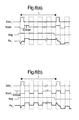
- Figures 7(a) and 7(b) illustrate schematically two inversion methods for driving an array of liquid crystal display cells.
- Figures 8(a) and 8(b) show typical signals for driving the dot inversion method and 1H inversion method respectively.
- the common connection COM is provided as a single plate which extends across all of the liquid crystal display cells. All of the liquid crystal display cells are connected to COM, but merely move up and down with the potential of COM unless their respective switches connect them to a respective signal line.
- the potential of COM oscillates between two predetermined potentials so as to cause the required inversion on the liquid crystal display cells from dot to dot or line to line and also from field/frame to field/frame.
- COM has a relatively high capacitance resulting in a relatively high power consumption for the driver.
- the drawn current I Ccom x Vcom x f(h) where Ccom is the capacitance of the COM plate, Vcom is the predetermined potential to which COM is driven and f(h) is the frequency of the change of the COM potential, for instance, the horizontal line frequency.
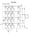
- the present invention follows a proposal to divide the conventional COM plate into an array of adjacent strips. This is illustrated schematically in Figures 9(a) and 9(b) . As illustrated, the common connection COM is provided as an array of strips 30, rather than as a single plate.
- each strip 30 Arranged along each strip 30 is a row of a plurality of liquid crystal cells 22.
- Each cell 22 is connected on one side to its corresponding COM strip 30 and, on the other side, to a respective switch 24.
- the switches 24 may be MOSFETs.
- all of the gates of the switches 24 of a row of cells 22 are connected to a respective gate line 26.
- each gate line can be used to control simultaneously all of the cells 22 of its respective row.
- the respective COM strip 30 can be driven to the required polarity suitable for writing to the cells 22 of that row/strip signals carried on the signal lines 28.
- a driving COM signal 32 is provided only to the COM strip 30 of the active line, namely the line made active by its respective gate line 26 enabling writing to the cells 22 of the respective row. All of the other COM strips 30 are provided with their stand-by COM signal 34.
- the driving COM signal 32 is provided as one of two potentials according to the inversion method
- the stand-by COM signal 34 is provided as a potential substantially midway between the two potentials used for the driving COM signal 32. In this way, when a non-active line becomes an active line, the charge required to bring the corresponding COM strip 30 to the required potential will always be reduced.
- FIG 10(a) illustrates schematically a liquid crystal display module 10 having a driver 40 provided alongside the display 16 itself.
- the driver 40 includes a shift register 42, ram 44, select SW46 and buffer 48.
- the driver 40 has a plurality of drive lines 50 each respectively connected to one of the COM strips 30.
- the driver 40 is thus able to drive consecutively each COM strip 30 with the active driving COM signal 32 having the appropriate potential for the inversion method, whilst driving all other COM strips 30 with the non-active drive or stand-by COM signal 34.
- Figure 9(c) illustrates schematically an arrangement for a colour display where pixels and sub-pixels are driven by a 1H inversion method in accordance with the embodiment described with reference to Figures 9(a) and (b) .
- FIG 9(d) when Gate1 is provided with an active pulse, its corresponding COM strip COM1 is driven to an appropriate potential (a low potential V 2 as illustrated) such that all of the pixels and pixel units along that COM strip can be written.
- Figure 9(d) illustrates writing to sub-pixels PixR1, G1 and B1.
- Gate2 is provided with an active pulse and COM strip COM2 is made active.
- the COM strip COM2 is provided with a voltage opposite to that previously provided to COM strip COM 1 (a high voltage V 3 as illustrated). All of the pixels and sub-pixels corresponding to Gate2 can then be written.
- Figure 9(d) illustrates writing only to sub-pixel PixB2.
- Figures 11(a) and 11(b) illustrate driving two consecutive frames on a liquid crystal display again using COM strips 30, but arranged for dot inversion rather than 1H inversion.
- each gate line 26 is not connected to all of the gates of the switches 24 of a row of liquid crystal display cells 22. Instead, each gate line 26 is connected to alternate switches 24 of one row and alternate (interlaced) switches 24 of an adjacent row.
- alternate cells 22 of one row can be driven by their signal lines 28 at the same time as the interlaced alternate cells 22 of the adjacent row are driven with their signal lines 28.
- both of the adjacent COM strips 30 corresponding to the two adjacent rows of liquid crystal display cells 22 are driven with the driving COM signal 32 to the appropriate potential. It does not matter that other liquid crystal display cells 22 are also connected to the two adjacent COM strips 30 which are driven to an active state, because those other liquid crystal display cells 22 have their switches 24 turned off and, hence, are in a floating state.
- both of such a pair of strips 30 are driven with the driving COM signal 32 simultaneously.
- all other COM strips 30 are provided with a stand-by COM signal 34, for instance of an intermediate potential midway between the two active COM voltages.
- a driver such as driver 40 of Figure 10(b) can be used with a liquid crystal display arranged in this way.
- Figure 12(a) illustrates schematically an arrangement for a colour display where individual pixel units or sub-pixels are driven in a dot inversion method.
- the individual pixel units or sub-pixels are connected to gate lines in an alternate manner in the same way as described for Figure 11(a) .
- sub-pixel PixG1 which is located between sub-pixels PixR1 and B1 is switched on.
- COM strip COM1 is driven with the opposite potential or inversion.
- the red and blue sub-pixels PixR2 and B2 can be written.
- Green sub-pixel PixG2 is written subsequently with Gate3.
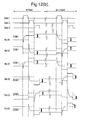
- Figure 13(a) illustrates an arrangement for colour display where the dot inversion method is applied pixel by pixel, with all three sub-pixels of a pixel having the same polarity.
- each gate line is connected to the switches of alternate pixels (each having three sub-pixels) in a row of sub-pixels with respective liquid crystal display cells.
- the same gate line is connected to alternate pixels of an adjacent row of sub-pixels with liquid crystal display cells in an interlaced manner.
- This arrangement can be driven as illustrated in Figure 13(b) .
- gate line Gate 1 carries a pulse to turn on the switches to which it is connected and COM strip COM1 is driven to an appropriate potential sub-pixels PixR1 and B1 can be driven by their signal lines. Although not illustrated, the sub-pixel between PixR1 and B1 can be driven at the same time.
- gate line Gate2 carries the active pulse
- the next pixel in the row becomes active.
- the COM strip COM1 is driven with the opposite polarity according to the dot inversion method and, as illustrated, sub-pixel PixG1 can be driven with its signal line. Although not illustrated, the sub-pixels either side of PixG1 can be driven at the same time.
- Figure 14(a) illustrates schematically a liquid crystal display having a sub-pixel and gate arrangement similar to that of Figure 12(a) . However, with the arrangement of Figure 14(a) , adjacent pairs of COM strips are connected together. Indeed, rather than providing an individual COM strip for each respective row of liquid crystal display cells, it is possible to provide half as many COM strips, each having twice the width such that each COM strip connects to two adjacent rows of liquid crystal display cells.
- Figure 14(b) illustrates schematically how such an arrangement can be driven.
- gate line Gate 1 When gate line Gate 1 carries an active pulse, sub-pixels PixR1 and B 1 will be turned on and with the large COM strip COM1 at an appropriate potential, the sub-pixels PixR1 and B 1 can be driven with their signal lines.
- large COM strip COM1 is again inverted and gate line Gate3 becomes active such that the switch for sub-pixel PixG2 is turned on and it becomes possible to drive that sub-pixel with its signal line.
- the large COM strip COM2 could also be activated so that sub-pixels PixR3 and B3 can be written.
- sub-pixels PixG3 and then PixG4 can be written.
Landscapes
- Engineering & Computer Science (AREA)
- Physics & Mathematics (AREA)
- General Physics & Mathematics (AREA)
- Crystallography & Structural Chemistry (AREA)
- Chemical & Material Sciences (AREA)
- Theoretical Computer Science (AREA)
- Computer Hardware Design (AREA)
- Nonlinear Science (AREA)
- Power Engineering (AREA)
- Microelectronics & Electronic Packaging (AREA)
- Mathematical Physics (AREA)
- Optics & Photonics (AREA)
- Liquid Crystal Display Device Control (AREA)
- Control Of Indicators Other Than Cathode Ray Tubes (AREA)
- Liquid Crystal (AREA)
Applications Claiming Priority (1)
| Application Number | Priority Date | Filing Date | Title |
|---|---|---|---|
| GB0806193A GB2458957B (en) | 2008-04-04 | 2008-04-04 | Liquid crystal display module |
Publications (2)
| Publication Number | Publication Date |
|---|---|
| EP2107549A2 true EP2107549A2 (fr) | 2009-10-07 |
| EP2107549A3 EP2107549A3 (fr) | 2010-09-22 |
Family
ID=39433170
Family Applications (1)
| Application Number | Title | Priority Date | Filing Date |
|---|---|---|---|
| EP09250779A Withdrawn EP2107549A3 (fr) | 2008-04-04 | 2009-03-20 | Module d'affichage à cristaux liquides |
Country Status (6)
| Country | Link |
|---|---|
| US (1) | US8456398B2 (fr) |
| EP (1) | EP2107549A3 (fr) |
| JP (1) | JP2009251608A (fr) |
| CN (1) | CN101551562B (fr) |
| GB (1) | GB2458957B (fr) |
| TW (1) | TW201003625A (fr) |
Families Citing this family (10)
| Publication number | Priority date | Publication date | Assignee | Title |
|---|---|---|---|---|
| GB2460090A (en) | 2008-05-16 | 2009-11-18 | Sony Corp | Ambient light detection device |
| JP2010256466A (ja) * | 2009-04-22 | 2010-11-11 | Sony Corp | 液晶表示装置およびその駆動方法 |
| JP2011008200A (ja) * | 2009-06-29 | 2011-01-13 | Sony Corp | 液晶表示装置およびその駆動方法 |
| US20120235984A1 (en) * | 2009-12-11 | 2012-09-20 | Sharp Kabushiki Kaisha | Display panel, liquid crystal display, and driving method |
| JP2012047807A (ja) | 2010-08-24 | 2012-03-08 | Sony Corp | 表示装置および電子機器 |
| KR101106141B1 (ko) * | 2010-09-17 | 2012-01-20 | 이성호 | 도트 인버전 방식의 액정패널 구동 방법 및 장치 |
| KR101872993B1 (ko) | 2011-03-28 | 2018-07-03 | 삼성디스플레이 주식회사 | 액정 표시 장치 |
| CN102231030B (zh) * | 2011-07-07 | 2013-04-10 | 南京中电熊猫液晶显示科技有限公司 | 薄膜晶体管液晶显示器的像素结构 |
| JP6154305B2 (ja) * | 2013-01-23 | 2017-06-28 | 株式会社ジャパンディスプレイ | 表示装置及び電子機器 |
| CN103399440A (zh) | 2013-08-08 | 2013-11-20 | 京东方科技集团股份有限公司 | 阵列基板、显示装置及驱动方法 |
Citations (3)
| Publication number | Priority date | Publication date | Assignee | Title |
|---|---|---|---|---|
| US20020154084A1 (en) | 2000-06-16 | 2002-10-24 | Yukio Tanaka | Active matrix display device, its driving method, and display element |
| US20050162363A1 (en) * | 2003-12-23 | 2005-07-28 | Kim Kyong S. | Liquid crystal display device and driving method thereof |
| US20050253829A1 (en) * | 2004-04-13 | 2005-11-17 | Norio Mamba | Display device and display device driving method |
Family Cites Families (27)
| Publication number | Priority date | Publication date | Assignee | Title |
|---|---|---|---|---|
| JP2568659B2 (ja) * | 1988-12-12 | 1997-01-08 | 松下電器産業株式会社 | 表示装置の駆動方法 |
| JPH05134629A (ja) * | 1991-11-12 | 1993-05-28 | Fujitsu Ltd | アクテイブマトリクス型液晶表示パネル及びその駆動方法 |
| JP3119942B2 (ja) * | 1992-07-22 | 2000-12-25 | 沖電気工業株式会社 | アクティブマトリクス型薄膜トランジスタ液晶パネルの駆動方法 |
| EP1134720A3 (fr) * | 1993-04-22 | 2002-02-27 | Matsushita Electric Industrial Co., Ltd. | Dispositif d'affichage et appareil d'affichage du type à projection qui l'utilise |
| JP3234131B2 (ja) | 1995-06-23 | 2001-12-04 | 株式会社東芝 | 液晶表示装置 |
| US6097361A (en) * | 1997-01-29 | 2000-08-01 | Advanced Micro Devices, Inc. | Photolithographic exposure system and method employing a liquid crystal display (LCD) panel as a configurable mask |
| KR100653751B1 (ko) | 1998-10-27 | 2006-12-05 | 샤프 가부시키가이샤 | 표시 패널의 구동 방법, 표시 패널의 구동 회로 및 액정 표시 장치 |
| US6489952B1 (en) * | 1998-11-17 | 2002-12-03 | Semiconductor Energy Laboratory Co., Ltd. | Active matrix type semiconductor display device |
| US6469684B1 (en) | 1999-09-13 | 2002-10-22 | Hewlett-Packard Company | Cole sequence inversion circuitry for active matrix device |
| WO2001073743A1 (fr) * | 2000-03-28 | 2001-10-04 | Seiko Epson Corporation | Afficheur a cristaux liquides, procede et dispositif de commande d'un afficheur a cristaux liquides, dispositif electronique |
| JP4137394B2 (ja) * | 2000-10-05 | 2008-08-20 | シャープ株式会社 | 表示装置の駆動方法、それを用いた表示装置、およびその表示装置を搭載した携帯機器 |
| TW493158B (en) * | 2001-05-29 | 2002-07-01 | Hannstar Display Corp | Transistor array circuit for liquid crystal display |
| US6864883B2 (en) * | 2001-08-24 | 2005-03-08 | Koninklijke Philips Electronics N.V. | Display device |
| JP3917845B2 (ja) * | 2001-11-16 | 2007-05-23 | シャープ株式会社 | 液晶表示装置 |
| KR100652215B1 (ko) * | 2003-06-27 | 2006-11-30 | 엘지.필립스 엘시디 주식회사 | 액정표시장치 |
| KR100997977B1 (ko) | 2004-01-12 | 2010-12-02 | 삼성전자주식회사 | 광센서 및 이를 이용한 표시 장치 |
| KR20060007972A (ko) | 2004-07-23 | 2006-01-26 | 삼성전자주식회사 | 표시장치 및 이의 휘도 제어방법 |
| KR101108391B1 (ko) * | 2004-12-31 | 2012-01-30 | 엘지디스플레이 주식회사 | 액정 표시장치 |
| US7605794B2 (en) | 2005-12-22 | 2009-10-20 | Nokia Corporation | Adjusting the refresh rate of a display |
| KR101177579B1 (ko) | 2005-12-30 | 2012-08-27 | 엘지디스플레이 주식회사 | 액정표시장치 및 그 구동방법 |
| JP5191639B2 (ja) * | 2006-09-15 | 2013-05-08 | 株式会社ジャパンディスプレイイースト | 液晶表示装置 |
| TWI356222B (en) * | 2006-09-18 | 2012-01-11 | Chimei Innolux Corp | Liquid crystal display panel and liquid crystal di |
| US7903107B2 (en) | 2007-06-18 | 2011-03-08 | Sony Ericsson Mobile Communications Ab | Adaptive refresh rate features |
| KR100924143B1 (ko) * | 2008-04-02 | 2009-10-28 | 삼성모바일디스플레이주식회사 | 평판표시장치 및 그의 구동 방법 |
| GB2458958B (en) | 2008-04-04 | 2010-07-07 | Sony Corp | Driving circuit for a liquid crystal display |
| GB2460090A (en) | 2008-05-16 | 2009-11-18 | Sony Corp | Ambient light detection device |
| GB2460409B (en) | 2008-05-27 | 2012-04-04 | Sony Corp | Driving circuit for a liquid crystal display |
-
2008
- 2008-04-04 GB GB0806193A patent/GB2458957B/en not_active Expired - Fee Related
-
2009
- 2009-03-17 TW TW098108598A patent/TW201003625A/zh unknown
- 2009-03-20 EP EP09250779A patent/EP2107549A3/fr not_active Withdrawn
- 2009-04-03 JP JP2009091615A patent/JP2009251608A/ja active Pending
- 2009-04-03 CN CN200910133832XA patent/CN101551562B/zh not_active Expired - Fee Related
- 2009-04-03 US US12/418,319 patent/US8456398B2/en not_active Expired - Fee Related
Patent Citations (3)
| Publication number | Priority date | Publication date | Assignee | Title |
|---|---|---|---|---|
| US20020154084A1 (en) | 2000-06-16 | 2002-10-24 | Yukio Tanaka | Active matrix display device, its driving method, and display element |
| US20050162363A1 (en) * | 2003-12-23 | 2005-07-28 | Kim Kyong S. | Liquid crystal display device and driving method thereof |
| US20050253829A1 (en) * | 2004-04-13 | 2005-11-17 | Norio Mamba | Display device and display device driving method |
Also Published As
| Publication number | Publication date |
|---|---|
| CN101551562B (zh) | 2012-10-31 |
| TW201003625A (en) | 2010-01-16 |
| GB2458957B (en) | 2010-11-24 |
| EP2107549A3 (fr) | 2010-09-22 |
| US20090251629A1 (en) | 2009-10-08 |
| CN101551562A (zh) | 2009-10-07 |
| GB2458957A (en) | 2009-10-07 |
| JP2009251608A (ja) | 2009-10-29 |
| US8456398B2 (en) | 2013-06-04 |
| GB0806193D0 (en) | 2008-05-14 |
Similar Documents
| Publication | Publication Date | Title |
|---|---|---|
| US8456398B2 (en) | Liquid crystal display module | |
| EP0466378B1 (fr) | Panneau d'affichage à cristal liquide avec scintillement réduit | |
| US7839374B2 (en) | Liquid crystal display device and method of driving the same | |
| CN110956921B (zh) | 阵列基板及其驱动方法、像素驱动装置、显示装置 | |
| CN107591144B (zh) | 显示面板的驱动方法以及驱动装置 | |
| JP2005018077A (ja) | 液晶表示装置及びその駆動方法 | |
| JP4420620B2 (ja) | 画像表示装置 | |
| CN107450225B (zh) | 显示面板及显示装置 | |
| CN102269905A (zh) | 液晶面板 | |
| CN111142298B (zh) | 阵列基板及显示装置 | |
| US7825886B2 (en) | Liquid crystal display device driven with a small number of data lines | |
| US7525527B2 (en) | Method for driving a liquid crystal display device | |
| US7777737B2 (en) | Active matrix type liquid crystal display device | |
| CN113299236A (zh) | 一种显示面板的驱动方法、装置和显示面板 | |
| KR20200030227A (ko) | 표시 장치 | |
| KR101074381B1 (ko) | 횡전계방식 액정표시장치 | |
| US8179392B2 (en) | Pre-charge system for on glass LCD driving circuit | |
| US20030107544A1 (en) | Display devices and driving method therefor | |
| US20100103086A1 (en) | Liquid crystal display panel for performing polarity inversion therein | |
| CN117711343B (zh) | 显示面板及其驱动方法、显示装置 | |
| KR20090106359A (ko) | 액정 디스플레이 모듈 | |
| KR100898789B1 (ko) | 액정표시장치의 구동방법 | |
| CN112068374B (zh) | 显示面板、显示装置及驱动方法 | |
| CN113674672B (zh) | 显示面板的驱动方法及显示面板 | |
| CN110444142B (zh) | 一种画素排列结构和面板 |
Legal Events
| Date | Code | Title | Description |
|---|---|---|---|
| PUAI | Public reference made under article 153(3) epc to a published international application that has entered the european phase |
Free format text: ORIGINAL CODE: 0009012 |
|
| AK | Designated contracting states |
Kind code of ref document: A2 Designated state(s): AT BE BG CH CY CZ DE DK EE ES FI FR GB GR HR HU IE IS IT LI LT LU LV MC MK MT NL NO PL PT RO SE SI SK TR |
|
| AX | Request for extension of the european patent |
Extension state: AL BA RS |
|
| PUAL | Search report despatched |
Free format text: ORIGINAL CODE: 0009013 |
|
| AK | Designated contracting states |
Kind code of ref document: A3 Designated state(s): AT BE BG CH CY CZ DE DK EE ES FI FR GB GR HR HU IE IS IT LI LT LU LV MC MK MT NL NO PL PT RO SE SI SK TR |
|
| AX | Request for extension of the european patent |
Extension state: AL BA RS |
|
| 17P | Request for examination filed |
Effective date: 20110321 |
|
| AKX | Designation fees paid |
Designated state(s): AT BE BG CH CY CZ DE DK EE ES FI FR GB GR HR HU IE IS IT LI LT LU LV MC MK MT NL NO PL PT RO SE SI SK TR |
|
| 17Q | First examination report despatched |
Effective date: 20110523 |
|
| STAA | Information on the status of an ep patent application or granted ep patent |
Free format text: STATUS: THE APPLICATION IS DEEMED TO BE WITHDRAWN |
|
| 18D | Application deemed to be withdrawn |
Effective date: 20140402 |