EP2107604A2 - Module semi-conducteur de puissance doté d'un circuit étanche hermétique et son procédé de fabrication - Google Patents
Module semi-conducteur de puissance doté d'un circuit étanche hermétique et son procédé de fabrication Download PDFInfo
- Publication number
- EP2107604A2 EP2107604A2 EP09004421A EP09004421A EP2107604A2 EP 2107604 A2 EP2107604 A2 EP 2107604A2 EP 09004421 A EP09004421 A EP 09004421A EP 09004421 A EP09004421 A EP 09004421A EP 2107604 A2 EP2107604 A2 EP 2107604A2
- Authority
- EP
- European Patent Office
- Prior art keywords
- power semiconductor
- layer
- sealing surface
- connection
- substrate
- Prior art date
- Legal status (The legal status is an assumption and is not a legal conclusion. Google has not performed a legal analysis and makes no representation as to the accuracy of the status listed.)
- Granted
Links
Images

Classifications
-
- H—ELECTRICITY
- H10—SEMICONDUCTOR DEVICES; ELECTRIC SOLID-STATE DEVICES NOT OTHERWISE PROVIDED FOR
- H10W—GENERIC PACKAGES, INTERCONNECTIONS, CONNECTORS OR OTHER CONSTRUCTIONAL DETAILS OF DEVICES COVERED BY CLASS H10
- H10W72/00—Interconnections or connectors in packages
-
- H—ELECTRICITY
- H10—SEMICONDUCTOR DEVICES; ELECTRIC SOLID-STATE DEVICES NOT OTHERWISE PROVIDED FOR
- H10W—GENERIC PACKAGES, INTERCONNECTIONS, CONNECTORS OR OTHER CONSTRUCTIONAL DETAILS OF DEVICES COVERED BY CLASS H10
- H10W76/00—Containers; Fillings or auxiliary members therefor; Seals
- H10W76/10—Containers or parts thereof
-
- H—ELECTRICITY
- H10—SEMICONDUCTOR DEVICES; ELECTRIC SOLID-STATE DEVICES NOT OTHERWISE PROVIDED FOR
- H10W—GENERIC PACKAGES, INTERCONNECTIONS, CONNECTORS OR OTHER CONSTRUCTIONAL DETAILS OF DEVICES COVERED BY CLASS H10
- H10W70/00—Package substrates; Interposers; Redistribution layers [RDL]
- H10W70/60—Insulating or insulated package substrates; Interposers; Redistribution layers
- H10W70/611—Insulating or insulated package substrates; Interposers; Redistribution layers for connecting multiple chips together
-
- H—ELECTRICITY
- H10—SEMICONDUCTOR DEVICES; ELECTRIC SOLID-STATE DEVICES NOT OTHERWISE PROVIDED FOR
- H10W—GENERIC PACKAGES, INTERCONNECTIONS, CONNECTORS OR OTHER CONSTRUCTIONAL DETAILS OF DEVICES COVERED BY CLASS H10
- H10W70/00—Package substrates; Interposers; Redistribution layers [RDL]
- H10W70/60—Insulating or insulated package substrates; Interposers; Redistribution layers
- H10W70/67—Insulating or insulated package substrates; Interposers; Redistribution layers characterised by their insulating layers or insulating parts
- H10W70/688—Flexible insulating substrates
-
- H—ELECTRICITY
- H10—SEMICONDUCTOR DEVICES; ELECTRIC SOLID-STATE DEVICES NOT OTHERWISE PROVIDED FOR
- H10W—GENERIC PACKAGES, INTERCONNECTIONS, CONNECTORS OR OTHER CONSTRUCTIONAL DETAILS OF DEVICES COVERED BY CLASS H10
- H10W72/00—Interconnections or connectors in packages
- H10W72/071—Connecting or disconnecting
- H10W72/077—Connecting of TAB connectors
-
- H—ELECTRICITY
- H10—SEMICONDUCTOR DEVICES; ELECTRIC SOLID-STATE DEVICES NOT OTHERWISE PROVIDED FOR
- H10W—GENERIC PACKAGES, INTERCONNECTIONS, CONNECTORS OR OTHER CONSTRUCTIONAL DETAILS OF DEVICES COVERED BY CLASS H10
- H10W72/00—Interconnections or connectors in packages
- H10W72/30—Die-attach connectors
-
- H—ELECTRICITY
- H10—SEMICONDUCTOR DEVICES; ELECTRIC SOLID-STATE DEVICES NOT OTHERWISE PROVIDED FOR
- H10W—GENERIC PACKAGES, INTERCONNECTIONS, CONNECTORS OR OTHER CONSTRUCTIONAL DETAILS OF DEVICES COVERED BY CLASS H10
- H10W72/00—Interconnections or connectors in packages
- H10W72/60—Strap connectors, e.g. thick copper clips for grounding of power devices
-
- H—ELECTRICITY
- H10—SEMICONDUCTOR DEVICES; ELECTRIC SOLID-STATE DEVICES NOT OTHERWISE PROVIDED FOR
- H10W—GENERIC PACKAGES, INTERCONNECTIONS, CONNECTORS OR OTHER CONSTRUCTIONAL DETAILS OF DEVICES COVERED BY CLASS H10
- H10W72/00—Interconnections or connectors in packages
- H10W72/701—Tape-automated bond [TAB] connectors
-
- H—ELECTRICITY
- H10—SEMICONDUCTOR DEVICES; ELECTRIC SOLID-STATE DEVICES NOT OTHERWISE PROVIDED FOR
- H10W—GENERIC PACKAGES, INTERCONNECTIONS, CONNECTORS OR OTHER CONSTRUCTIONAL DETAILS OF DEVICES COVERED BY CLASS H10
- H10W74/00—Encapsulations, e.g. protective coatings
- H10W74/40—Encapsulations, e.g. protective coatings characterised by their materials
- H10W74/47—Encapsulations, e.g. protective coatings characterised by their materials comprising organic materials, e.g. plastics or resins
- H10W74/476—Organic materials comprising silicon
-
- H—ELECTRICITY
- H10—SEMICONDUCTOR DEVICES; ELECTRIC SOLID-STATE DEVICES NOT OTHERWISE PROVIDED FOR
- H10W—GENERIC PACKAGES, INTERCONNECTIONS, CONNECTORS OR OTHER CONSTRUCTIONAL DETAILS OF DEVICES COVERED BY CLASS H10
- H10W76/00—Containers; Fillings or auxiliary members therefor; Seals
- H10W76/10—Containers or parts thereof
- H10W76/12—Containers or parts thereof characterised by their shape
- H10W76/13—Containers comprising a conductive base serving as an interconnection
- H10W76/138—Containers comprising a conductive base serving as an interconnection having another interconnection being formed by a cover plate parallel to the conductive base, e.g. sandwich type
-
- H—ELECTRICITY
- H10—SEMICONDUCTOR DEVICES; ELECTRIC SOLID-STATE DEVICES NOT OTHERWISE PROVIDED FOR
- H10W—GENERIC PACKAGES, INTERCONNECTIONS, CONNECTORS OR OTHER CONSTRUCTIONAL DETAILS OF DEVICES COVERED BY CLASS H10
- H10W90/00—Package configurations
-
- H—ELECTRICITY
- H10—SEMICONDUCTOR DEVICES; ELECTRIC SOLID-STATE DEVICES NOT OTHERWISE PROVIDED FOR
- H10W—GENERIC PACKAGES, INTERCONNECTIONS, CONNECTORS OR OTHER CONSTRUCTIONAL DETAILS OF DEVICES COVERED BY CLASS H10
- H10W90/00—Package configurations
- H10W90/401—Package configurations characterised by multiple insulating or insulated package substrates, interposers or RDLs
-
- H—ELECTRICITY
- H10—SEMICONDUCTOR DEVICES; ELECTRIC SOLID-STATE DEVICES NOT OTHERWISE PROVIDED FOR
- H10W—GENERIC PACKAGES, INTERCONNECTIONS, CONNECTORS OR OTHER CONSTRUCTIONAL DETAILS OF DEVICES COVERED BY CLASS H10
- H10W72/00—Interconnections or connectors in packages
- H10W72/071—Connecting or disconnecting
- H10W72/073—Connecting or disconnecting of die-attach connectors
- H10W72/07331—Connecting techniques
- H10W72/07336—Soldering or alloying
-
- H—ELECTRICITY
- H10—SEMICONDUCTOR DEVICES; ELECTRIC SOLID-STATE DEVICES NOT OTHERWISE PROVIDED FOR
- H10W—GENERIC PACKAGES, INTERCONNECTIONS, CONNECTORS OR OTHER CONSTRUCTIONAL DETAILS OF DEVICES COVERED BY CLASS H10
- H10W72/00—Interconnections or connectors in packages
- H10W72/071—Connecting or disconnecting
- H10W72/076—Connecting or disconnecting of strap connectors
- H10W72/07631—Techniques
-
- H—ELECTRICITY
- H10—SEMICONDUCTOR DEVICES; ELECTRIC SOLID-STATE DEVICES NOT OTHERWISE PROVIDED FOR
- H10W—GENERIC PACKAGES, INTERCONNECTIONS, CONNECTORS OR OTHER CONSTRUCTIONAL DETAILS OF DEVICES COVERED BY CLASS H10
- H10W72/00—Interconnections or connectors in packages
- H10W72/60—Strap connectors, e.g. thick copper clips for grounding of power devices
- H10W72/651—Materials of strap connectors
- H10W72/652—Materials of strap connectors comprising metals or metalloids, e.g. silver
-
- H—ELECTRICITY
- H10—SEMICONDUCTOR DEVICES; ELECTRIC SOLID-STATE DEVICES NOT OTHERWISE PROVIDED FOR
- H10W—GENERIC PACKAGES, INTERCONNECTIONS, CONNECTORS OR OTHER CONSTRUCTIONAL DETAILS OF DEVICES COVERED BY CLASS H10
- H10W72/00—Interconnections or connectors in packages
- H10W72/90—Bond pads, in general
- H10W72/921—Structures or relative sizes of bond pads
- H10W72/926—Multiple bond pads having different sizes
-
- H—ELECTRICITY
- H10—SEMICONDUCTOR DEVICES; ELECTRIC SOLID-STATE DEVICES NOT OTHERWISE PROVIDED FOR
- H10W—GENERIC PACKAGES, INTERCONNECTIONS, CONNECTORS OR OTHER CONSTRUCTIONAL DETAILS OF DEVICES COVERED BY CLASS H10
- H10W72/00—Interconnections or connectors in packages
- H10W72/90—Bond pads, in general
- H10W72/941—Dispositions of bond pads
- H10W72/944—Dispositions of multiple bond pads
-
- H—ELECTRICITY
- H10—SEMICONDUCTOR DEVICES; ELECTRIC SOLID-STATE DEVICES NOT OTHERWISE PROVIDED FOR
- H10W—GENERIC PACKAGES, INTERCONNECTIONS, CONNECTORS OR OTHER CONSTRUCTIONAL DETAILS OF DEVICES COVERED BY CLASS H10
- H10W90/00—Package configurations
- H10W90/701—Package configurations characterised by the relative positions of pads or connectors relative to package parts
- H10W90/761—Package configurations characterised by the relative positions of pads or connectors relative to package parts of strap connectors
- H10W90/764—Package configurations characterised by the relative positions of pads or connectors relative to package parts of strap connectors between a chip and a stacked insulating package substrate, interposer or RDL
Definitions
- the invention describes a power semiconductor module and a manufacturing method for this purpose, wherein the circuit arrangement of the power semiconductor module is hermetically sealed against environmental influences. Especially when using electric drives in vehicles or other applications in harsh environments, it is advantageous to form the power semiconductor module particularly. This design was intended to protect the circuit arrangement of the power semiconductor module from the effects of high temperature fluctuations, especially in combination with moisture.
- prepregs are known power semiconductor modules according to the DE 196 17 055 C1 wherein so-called prepregs are disclosed for internal isolation of the power semiconductor module.
- prepregs which cure under pressure and / or temperature and thus form a material connection with at least one connection partner.
- connection means of an alternating sequence of conductive and insulating layers for circuit-compatible connection of the circuit arrangement of a power semiconductor module.
- Such connection devices are particularly preferred for compact structures of power semiconductor modules.
- disk cells have long been known which have one or more hermetically sealed against environmental influences power semiconductor components in their interior.
- Such disc cells usually have no complex circuit arrangements, such as three-phase bridge circuits, as they are known from power semiconductor modules with plastic housings.
- the invention has for its object to provide a power semiconductor module and a manufacturing method thereof, wherein the circuit arrangement of the power semiconductor module is hermetically sealed against environmental influences and wherein the circuit arrangement is simultaneously accessible to a flexible design with ease of manufacture.
- the starting point of the invention is a circuit arrangement of a power semiconductor module with a substrate, with conductor tracks arranged thereon and power semiconductor components arranged thereon, and with a connecting device arranged for this purpose.
- the term circuit arrangement is understood to be the sum of all conductor tracks and semiconductor components required for the electrical function.
- the connecting device used here is an alternating layer sequence of at least two electrically conductive layers and at least one electrically insulating layer.
- the interconnects of the circuit arrangement are formed on the substrate and electrically isolated from each other. They carry the power semiconductor components and form part of the circuit-compatible connections of the power semiconductor components.
- the other circuit-compliant connections are by means of the connection device educated.
- at least one of the electrically conductive layers is structured in itself and forms connecting tracks. It may also be preferred if vias are provided between different electrically conductive layers.
- the substrate has a first sealing surface surrounding the circuit arrangement without interruption.
- This can be configured as a frame around the circuit arrangement and can be embodied, for example, as a metallic layer analogous to the conductor tracks or as a free area on the substrate.
- This first sealing surface is hermetically sealed by means of a connecting layer with an associated second sealing surface of the connecting device, either on a metallic or an insulating layer.
- This compound is preferably formed as a pressure sintered connection.
- the term of the pressure sintered connection not only as the known compound of two metals by means of a sintered metal but also the electrically insulating compound with a prepreg instead of the sintered metal, wherein the temperature and pressure conditions during the formation of the compound those of a known pressure sintered compound comply with sintered metal.
- a gel-like insulating material for example a silicone gel, is arranged.
- Fig. 1 shows a section of a power semiconductor module with a connecting device according to the prior art in side view.
- Fig. 2 shows a section of a power semiconductor module with a connecting device according to the prior art in plan view.
- Fig. 3 shows a detail of a first embodiment of a power semiconductor module according to the invention in side view.
- Fig. 4 shows a section of a second embodiment of a power semiconductor module according to the invention in side view.
- Fig. 5 shows a detail of a third embodiment of a power semiconductor module according to the invention in side view.
- Fig. 6 shows a plan view of a substrate of a power semiconductor module according to the invention.
- Fig. 7 shows a section of a first connection means of a power semiconductor module according to the invention.
- Fig. 8 shows a section of a second connection device of a power semiconductor module according to the invention.
- Fig. 1 shows a section of a power semiconductor module with a connecting device (4) according to the prior art in side view.
- a substrate (2) Shown here is a substrate (2), as it is often known as so-called. DCB (direct copper bonding) or IMS (insulated metal substrate) substrate, without this being a limitation to such substrates.
- the substrate (2) has an insulating layer (20) arranged thereon and electrically insulated from each other conductor tracks (22 a / b).
- One of these conductor tracks (22a) carries here a unhoused semiconductor component (3), for example a power transistor as it is used by way of example for driving three-phase motors.
- a sintered metal layer (52) is arranged for the electrically conductive connection between the first conductor (22a) carrying the semiconductor component (3) and an associated contact surface (32) on the first main surface of the semiconductor component (3).
- This sintered metal layer (52) constitutes an electrically conductive connection of high reliability after the pressure sintering process of manufacture.
- the second main surface of the semiconductor component (3) has two contact surfaces (34, 36).
- the connecting device (4) is designed here as a metallic foil (40), preferably made of copper with a noble metal coating in the region of the sintered connections (50, 52).
- the thickness of this metallic foil (40) is chosen such that it has at least the same current carrying capacity as a wire bonding connection according to the prior art.
- connection device (4) represents the electrically conductive connection between the emitter connection surface (34) of the semiconductor component (3) and a second conductor track (22b) of the substrate (2).
- the connection of the connection device (4) to the second conductor track (22b) is likewise designed as a pressure sintered connection.
- the metallic foil (40) has an arcuate course (420) between the two contact surfaces.
- an insulating material (6) is arranged in the volume region formed by the arcuate course (420) of the connecting device (4), the substrate (2) and the semiconductor device (3). This insulating material was applied during the manufacturing process in those areas which is then covered by a connecting device (4). In this embodiment, this is the area in addition to the lateral edge (30) of the semiconductor component (3) and an outer part of the upper edge (38), cf. Fig. 2 ,
- the insulating material used (6) is a multi-component silicone compound which has been applied in a metering or casting process at the edge of the semiconductor device (3) and was crosslinked by means of a UV exposure.
- a certain toughness of the insulating material (6) is given, and on the other hand, such a silicone compound is also suitable for internal insulation, if the circuit arrangement has been designed for correspondingly high voltages.
- Fig. 2 shows a section of a power semiconductor module with a connecting device according to the prior art in plan view. Shown here are the same parts of Wegungsanorndung as under Fig. 1 described.
- the insulating material (6) serves on the one hand in a two-dimensional pressure introduction in the context of Drucksintertress in the direction of the drawing plane as quasihydostatic element which distributes the pressure evenly at its interfaces and thus prevents damage to the semiconductor device during pressurization.
- the insulating material (6) also serves the already described electrical insulation of the circuit arrangement of the power semiconductor module according to the invention.
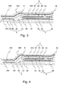
- Fig. 3 shows a detail of a first embodiment of a power semiconductor module according to the invention in side view.
- the basic structure of the substrate (2) as well as the power semiconductor device (3) arranged on the conductor track (22) is identical to that of FIG Fig. 1 described.
- the connecting device (4) here has an alternating construction of at least three layers, the layer sequence starting from the substrate (2) starting with a first electrically conductive layer (40), to which a first insulating (44) and then another conductive layer (42) follows.
- the connecting device (4) extends beyond the entire circuit arrangement and beyond the first sealing surface (200), cf. Fig. 6 ,
- the substrate (2) has a sealing surface (200) formed only peripherally around the circuit arrangement, which is arranged here on a metallic layer (24) formed analogously to the conductor tracks (22).
- a sintered metal layer (60) is arranged on the first, here metallic sealing surface (200), which in a pressure sintering process with the second sealing surface (400), here on the first conductive layer (40) of Connecting device (4) is arranged connected.
- the connection partners that is to say the first (200) and second sealing surfaces (400), with a noble metal coating.
- a gel-type insulating material (6) is arranged circumferentially around the respective power semiconductor components (3), advantageously up to the first sealing surface (200). This encloses the power semiconductor component (3) not only at its outer edge (30) but also covers its main surface facing away from the subrate at its edge (38).
- Fig. 4 shows a section of a second embodiment of a power semiconductor module according to the invention in side view.
- the design of the power semiconductor component (3) and the structure of the connecting device (4) are largely identical to those of Fig. 3 described.
- the connection device projects at least partially further beyond the first sealing surface (200) on the side facing away from the power semiconductor component (3) in order, for example, to be connected to connection elements for external load and auxiliary connections.
- the substrate (2) does not have a metallic layer as the first sealing surface (200) but exclusively a region of the base body (20) of the substrate (2) completely enclosing the circuit arrangement, ie a region on the DCB substrate ceramics.
- Sintered metal can again be used here as connecting layer (60), in which case, however, a noble metal coating would have to be deposited on the respective sealing surface (200, 400).
- a bonding layer (60) is a prepreg, which is arranged like a frame around the circuit around and thus completely encloses the circuit arrangement (see. Fig. 6 ).
- the connection of the prepreg (60) with the first (200) and second sealing surface (400) is also created at the same time, wherein the second sealing surface (400) again has a partial surface of the first electrically conductive layer (40) of the connecting device (4).
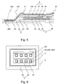
- Fig. 5 shows a detail of a third embodiment of a power semiconductor module according to the invention in side view. This differs from the second embodiment according to Fig. 4 in that the second sealing surface (400) is part of the first insulating layer (44) of the connecting device (4).
- the connecting layer (60) is advantageously designed as a prepreg.
- Fig. 6 shows a plan view of a substrate (2) of a power semiconductor module according to the invention. Shown here is the substrate (2) with the circuit arrangement consisting of three printed conductors (22) and arranged on two of these printed conductors power semiconductor components (3). Also shown schematically is the connecting layer (4), which is congruent with the circumferential first sealing surface (200) on the substrate (2) and the second sealing surface (400) on the connecting device (4).
- circuit-compatible connection of the power semiconductor components (3) with one another or with a further conductor track (22) is effected by the connecting device (4) shown only in outline. It can be seen that this invention, the entire circuit arrangement and the first sealing surface (200) surmounted in order to achieve a hermetically sealed termination of the circuit to environmental influences.
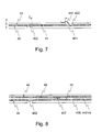
- Fig. 7 shows a section of a first connection device (4) of a power semiconductor module according to the invention. Shown here is a via (404) from the interrupted (422) second electrically conductive layer (42) through a recess (442) of the insulating layer (44) to the first electrically conductive layer (40). This is here designed as a wire bond connection (404). Also shown is an interruption (402) of the first electrically conductive layer (40), by way of example for producing two mutually insulated connection paths for the emitter connection and the gate connection of a power semiconductor component, cf. Fig. 3 to 5 ).
- the circumferential first and second sealing surfaces it may not only be necessary to connect the circumferential first and second sealing surfaces, but also to provide a spacing (x) between openings (402, 422) of the electrically conductive layers (40, 42). It is thus particularly preferred if two such openings (40, 42) have a distance (x) from one another which has at least ten times the thickness (d) of the insulating layer (44) arranged between the electrically conductive layers (40, 42) ,
- Fig. 8 shows a section of a second connection device (4) of a power semiconductor module according to the invention. Shown here is a connection device with three electrically conductive layers (40, 42, 46) and two insulating layers (44, 48) arranged between each.
- the first and second electrically conductive layers (40, 42) have plated-through holes (406) for the circuit-compatible connection, while the third electrically conductive layer (46) is uninterrupted and can serve as an example for shielding the circuit arrangement.
- Each of the individual layers of this connection device is suitable for arranging the second sealing surface (400) thereon.
Landscapes
- Structures Or Materials For Encapsulating Or Coating Semiconductor Devices Or Solid State Devices (AREA)
- Combinations Of Printed Boards (AREA)
- Structure Of Printed Boards (AREA)
Applications Claiming Priority (1)
| Application Number | Priority Date | Filing Date | Title |
|---|---|---|---|
| DE102008017454A DE102008017454B4 (de) | 2008-04-05 | 2008-04-05 | Leistungshalbleitermodul mit hermetisch dichter Schaltungsanordnung und Herstellungsverfahren hierzu |
Publications (3)
| Publication Number | Publication Date |
|---|---|
| EP2107604A2 true EP2107604A2 (fr) | 2009-10-07 |
| EP2107604A3 EP2107604A3 (fr) | 2010-11-03 |
| EP2107604B1 EP2107604B1 (fr) | 2014-09-10 |
Family
ID=40886253
Family Applications (1)
| Application Number | Title | Priority Date | Filing Date |
|---|---|---|---|
| EP09004421.5A Active EP2107604B1 (fr) | 2008-04-05 | 2009-03-27 | Module semi-conducteur de puissance doté d'un circuit étanche hermétique et son procédé de fabrication |
Country Status (6)
| Country | Link |
|---|---|
| US (1) | US8324717B2 (fr) |
| EP (1) | EP2107604B1 (fr) |
| JP (1) | JP5537825B2 (fr) |
| KR (1) | KR101574343B1 (fr) |
| CN (1) | CN101552255B (fr) |
| DE (1) | DE102008017454B4 (fr) |
Cited By (2)
| Publication number | Priority date | Publication date | Assignee | Title |
|---|---|---|---|---|
| EP2747133A3 (fr) * | 2012-12-19 | 2018-01-03 | General Electric Company | Emballage de module d'énergie avec reservoir de liquide de refroidissement |
| US20220285281A1 (en) * | 2020-02-27 | 2022-09-08 | Micron Technology, Inc. | Semiconductor devices with flexible connector array |
Families Citing this family (18)
| Publication number | Priority date | Publication date | Assignee | Title |
|---|---|---|---|---|
| DE102008017454B4 (de) | 2008-04-05 | 2010-02-04 | Semikron Elektronik Gmbh & Co. Kg | Leistungshalbleitermodul mit hermetisch dichter Schaltungsanordnung und Herstellungsverfahren hierzu |
| DE102009024385B4 (de) * | 2009-06-09 | 2011-03-17 | Semikron Elektronik Gmbh & Co. Kg | Verfahren zur Herstellung eines Leistungshalbleitermoduls und Leistungshalbleitermodul mit einer Verbindungseinrichtung |
| DE102010038731B3 (de) * | 2010-07-30 | 2011-12-08 | Semikron Elektronik Gmbh & Co. Kg | Submodul und Leistungshalbleitermodul |
| DE102010039824B4 (de) * | 2010-08-26 | 2018-03-29 | Semikron Elektronik Gmbh & Co. Kg | Leistungsbaugruppe mit einer flexiblen Verbindungseinrichtung |
| DE102010062547B4 (de) * | 2010-12-07 | 2021-10-28 | Semikron Elektronik Gmbh & Co. Kg | Verfahren zur Herstellung einer Schaltungsanordnung |
| KR102034717B1 (ko) * | 2013-02-07 | 2019-10-21 | 삼성전자주식회사 | 파워모듈용 기판, 파워모듈용 터미널 및 이들을 포함하는 파워모듈 |
| DE102013102828B4 (de) * | 2013-03-20 | 2018-04-12 | Semikron Elektronik Gmbh & Co. Kg | Leistungsbaugruppe mit einer als Folienverbund ausgebildeten Verbindungseinrichtung |
| DE102014214057A1 (de) * | 2014-07-18 | 2016-01-21 | Zf Friedrichshafen Ag | Elektronische Getriebesteuerungseinrichtung und Verfahren zum Herstellen derselben |
| DE102014114093B4 (de) | 2014-09-29 | 2017-03-23 | Danfoss Silicon Power Gmbh | Verfahren zum Niedertemperatur-Drucksintern |
| DE102014114097B4 (de) | 2014-09-29 | 2017-06-01 | Danfoss Silicon Power Gmbh | Sinterwerkzeug und Verfahren zum Sintern einer elektronischen Baugruppe |
| US10056319B2 (en) | 2016-04-29 | 2018-08-21 | Delta Electronics, Inc. | Power module package having patterned insulation metal substrate |
| DE102017215039A1 (de) * | 2017-08-29 | 2019-02-28 | Siemens Aktiengesellschaft | Leistungsmodul und Verfahren zur Herstellung eines solchen Leistungsmoduls |
| JP6939542B2 (ja) * | 2017-12-28 | 2021-09-22 | 株式会社オートネットワーク技術研究所 | 電気接続装置 |
| DE102019112477B4 (de) * | 2019-05-13 | 2024-03-14 | Semikron Elektronik Gmbh & Co. Kg | Leistungshalbleiterbauelement mit einer Kontakteinrichtung |
| DE102020121033B4 (de) * | 2020-08-10 | 2024-08-29 | Semikron Elektronik Gmbh & Co. Kg | Leistungselektronische Schalteinrichtung, Leistungshalbleitermodul damit und Verfahren zur Herstellung |
| JP7809922B2 (ja) * | 2021-06-16 | 2026-02-03 | 富士電機株式会社 | 半導体装置 |
| DE102021123636B4 (de) * | 2021-09-13 | 2024-01-25 | Semikron Elektronik Gmbh & Co. Kg | Leistungshalbleitermodul mit einer Substratanordnung, mit Leistungshalbleiterbauelementen und mit einer Folienstapelanordnung |
| DE102022125597A1 (de) * | 2022-10-05 | 2024-04-11 | Semikron Elektronik Gmbh & Co. Kg | Leistungselektronische Anordnung und Leistungshalbleitermodul hiermit |
Citations (3)
| Publication number | Priority date | Publication date | Assignee | Title |
|---|---|---|---|---|
| DE19617055C1 (de) | 1996-04-29 | 1997-06-26 | Semikron Elektronik Gmbh | Halbleiterleistungsmodul hoher Packungsdichte in Mehrschichtbauweise |
| DE10355925A1 (de) | 2003-11-29 | 2005-06-30 | Semikron Elektronik Gmbh | Leistungshalbleitermodul und Verfahren seiner Herstellung |
| DE102004021927A1 (de) | 2004-05-04 | 2005-12-01 | Semikron Elektronik Gmbh & Co. Kg | Verfahren zur inneren elektrischen Isolation eines Substrats für ein Leistungshalbleitermodul |
Family Cites Families (14)
| Publication number | Priority date | Publication date | Assignee | Title |
|---|---|---|---|---|
| DE1594165A1 (de) * | 1966-01-12 | 1971-02-04 | Metallgesellschaft Ag | Haftmittel fuer die Bindung von Kautschuk auf Werkstoffen |
| JPH04139737A (ja) * | 1990-09-29 | 1992-05-13 | Toshiba Lighting & Technol Corp | 半導体チップの実装方法 |
| US5637922A (en) * | 1994-02-07 | 1997-06-10 | General Electric Company | Wireless radio frequency power semiconductor devices using high density interconnect |
| DE59713027D1 (de) * | 1996-09-30 | 2010-03-25 | Infineon Technologies Ag | Mikroelektronisches bauteil in sandwich-bauweise |
| CA2255441C (fr) * | 1997-12-08 | 2003-08-05 | Hiroki Sekiya | Boitier pour dispositif d'alimentation a semiconducteurs et methode d'assemblage connexe |
| DE10314172B4 (de) * | 2003-03-28 | 2006-11-30 | Infineon Technologies Ag | Verfahren zum Betreiben einer Anordnung aus einem elektrischen Bauelement auf einem Substrat und Verfahren zum Herstellen der Anordnung |
| US7023078B2 (en) * | 2003-05-06 | 2006-04-04 | Seiko Instruments Inc. | Packages for communication devices |
| WO2005096374A1 (fr) * | 2004-03-15 | 2005-10-13 | Siemens Aktiengesellschaft | Produit electrotechnique comprenant un element electrique et une masse de scellement pour l'isolation electrique de l'element, et procede de fabrication associe |
| DE102004057421B4 (de) * | 2004-11-27 | 2009-07-09 | Semikron Elektronik Gmbh & Co. Kg | Druckkontaktiertes Leistungshalbleitermodul für hohe Umgebungstemperaturen und Verfahren zu seiner Herstellung |
| DE102004061936A1 (de) * | 2004-12-22 | 2006-07-06 | Siemens Ag | Anordnung eines Halbleitermoduls und einer elektrischen Verschienung |
| DE102005047567B3 (de) * | 2005-10-05 | 2007-03-29 | Semikron Elektronik Gmbh & Co. Kg | Leistungshalbleitermodul mit Isolationszwischenlage und Verfahren zu seiner Herstellung |
| JP4598687B2 (ja) * | 2006-02-09 | 2010-12-15 | 株式会社日立製作所 | 金属超微粒子使用接合材及びそれを用いた半導体装置 |
| DE102007006706B4 (de) * | 2007-02-10 | 2011-05-26 | Semikron Elektronik Gmbh & Co. Kg | Schaltungsanordnung mit Verbindungseinrichtung sowie Herstellungsverfahren hierzu |
| DE102008017454B4 (de) | 2008-04-05 | 2010-02-04 | Semikron Elektronik Gmbh & Co. Kg | Leistungshalbleitermodul mit hermetisch dichter Schaltungsanordnung und Herstellungsverfahren hierzu |
-
2008
- 2008-04-05 DE DE102008017454A patent/DE102008017454B4/de active Active
-
2009
- 2009-03-25 JP JP2009073924A patent/JP5537825B2/ja active Active
- 2009-03-27 EP EP09004421.5A patent/EP2107604B1/fr active Active
- 2009-04-02 CN CN2009101330510A patent/CN101552255B/zh active Active
- 2009-04-03 KR KR1020090028914A patent/KR101574343B1/ko active Active
- 2009-04-06 US US12/384,508 patent/US8324717B2/en active Active
Patent Citations (3)
| Publication number | Priority date | Publication date | Assignee | Title |
|---|---|---|---|---|
| DE19617055C1 (de) | 1996-04-29 | 1997-06-26 | Semikron Elektronik Gmbh | Halbleiterleistungsmodul hoher Packungsdichte in Mehrschichtbauweise |
| DE10355925A1 (de) | 2003-11-29 | 2005-06-30 | Semikron Elektronik Gmbh | Leistungshalbleitermodul und Verfahren seiner Herstellung |
| DE102004021927A1 (de) | 2004-05-04 | 2005-12-01 | Semikron Elektronik Gmbh & Co. Kg | Verfahren zur inneren elektrischen Isolation eines Substrats für ein Leistungshalbleitermodul |
Cited By (3)
| Publication number | Priority date | Publication date | Assignee | Title |
|---|---|---|---|---|
| EP2747133A3 (fr) * | 2012-12-19 | 2018-01-03 | General Electric Company | Emballage de module d'énergie avec reservoir de liquide de refroidissement |
| US20220285281A1 (en) * | 2020-02-27 | 2022-09-08 | Micron Technology, Inc. | Semiconductor devices with flexible connector array |
| US11908803B2 (en) * | 2020-02-27 | 2024-02-20 | Micron Technology, Inc. | Semiconductor devices with flexible connector array |
Also Published As
| Publication number | Publication date |
|---|---|
| US20100090328A1 (en) | 2010-04-15 |
| JP2009253280A (ja) | 2009-10-29 |
| US8324717B2 (en) | 2012-12-04 |
| EP2107604B1 (fr) | 2014-09-10 |
| EP2107604A3 (fr) | 2010-11-03 |
| KR101574343B1 (ko) | 2015-12-03 |
| KR20090106354A (ko) | 2009-10-08 |
| JP5537825B2 (ja) | 2014-07-02 |
| DE102008017454A1 (de) | 2009-12-31 |
| CN101552255B (zh) | 2012-11-14 |
| DE102008017454B4 (de) | 2010-02-04 |
| CN101552255A (zh) | 2009-10-07 |
Similar Documents
| Publication | Publication Date | Title |
|---|---|---|
| EP2107604B1 (fr) | Module semi-conducteur de puissance doté d'un circuit étanche hermétique et son procédé de fabrication | |
| EP1956647B1 (fr) | Circuit doté d'un dispositif de liaison et son procédé de fabrication | |
| EP1255299B1 (fr) | Module semiconducteur de puissance avec contact à pression | |
| EP1898466A2 (fr) | Circuit semi-conducteur dans un boîtier doté d'un dispositif de contact | |
| EP1841299A2 (fr) | Dispositif de liaison pour composant électrique | |
| DE102005047567B3 (de) | Leistungshalbleitermodul mit Isolationszwischenlage und Verfahren zu seiner Herstellung | |
| EP2040295A2 (fr) | Agencement doté d'un dispositif de liaison et d'au moins un composant semi-conducteur | |
| DE102015116165A1 (de) | Verfahren zur Herstellung einer leistungselektronischen Schalteinrichtung und leistungselektronische Schalteinrichtung | |
| DE102011080153A1 (de) | Flexible verbindung von substraten in leistungshalbleitermodulen | |
| DE102013108185B4 (de) | Verfahren zur Herstellung einer leistungselektronischen Schalteinrichtung und leistungselektronische Schalteinrichtung | |
| EP2055155A1 (fr) | Appareil de commande pour véhicule automobile | |
| EP3979313B1 (fr) | Dispositif électronique de puissance et module semi-conducteur de puissance correspondant | |
| DE102009024385B4 (de) | Verfahren zur Herstellung eines Leistungshalbleitermoduls und Leistungshalbleitermodul mit einer Verbindungseinrichtung | |
| DE102011078806B4 (de) | Herstellungsverfahren für ein leistungselektronisches System mit einer Kühleinrichtung | |
| DE102010002945A1 (de) | Schaltungsanordnung und zugehöriges steuergerät für ein kraftfahrzeug | |
| DE102008026347B4 (de) | Leistungselektronische Anordnung mit einem Substrat und einem Grundkörper | |
| EP3338302A1 (fr) | Carte de circuits imprimés et ensemble électronique de puissance équipé d'une carte de circuits imprimés | |
| DE102014203306A1 (de) | Herstellen eines Elektronikmoduls | |
| DE102023113073B4 (de) | Leistungshalbleiterbauelement mit Kontakteinrichtung und Herstellungsverfahren hierfür | |
| DE102009050178B3 (de) | Leistungshalbleitermodul mit einem eine dreidimensionale Oberflächenkontur aufweisenden Substrat sowie Herstellungsverfahren hierzu | |
| DE102010012457B4 (de) | Schaltungsanordnung mit einer elektrischen Komponente und einer Verbundfolie | |
| DE102022111579A1 (de) | Verfahren zur Herstellung einer leistungselektronischen Schalteinrichtung und leistungselektronische Schalteinrichtung | |
| DE102010062453A1 (de) | Halbleiterbauelement mit erhöhter Stabilität gegenüber thermomechanischen Einflüssen sowie Verfahren zur Kontaktierung eines Halbleiters | |
| DE102015213085A1 (de) | Leistungsmodul sowie Verfahren zum Herstellen eines Leistungsmoduls | |
| DE102015212092A1 (de) | Elektronische Komponente und Verfahren zu deren Herstellung |
Legal Events
| Date | Code | Title | Description |
|---|---|---|---|
| PUAI | Public reference made under article 153(3) epc to a published international application that has entered the european phase |
Free format text: ORIGINAL CODE: 0009012 |
|
| AK | Designated contracting states |
Kind code of ref document: A2 Designated state(s): AT BE BG CH CY CZ DE DK EE ES FI FR GB GR HR HU IE IS IT LI LT LU LV MC MK MT NL NO PL PT RO SE SI SK TR |
|
| AX | Request for extension of the european patent |
Extension state: AL BA RS |
|
| PUAL | Search report despatched |
Free format text: ORIGINAL CODE: 0009013 |
|
| AK | Designated contracting states |
Kind code of ref document: A3 Designated state(s): AT BE BG CH CY CZ DE DK EE ES FI FR GB GR HR HU IE IS IT LI LT LU LV MC MK MT NL NO PL PT RO SE SI SK TR |
|
| AX | Request for extension of the european patent |
Extension state: AL BA RS |
|
| RIC1 | Information provided on ipc code assigned before grant |
Ipc: H01L 21/60 20060101ALI20100930BHEP Ipc: H01L 23/538 20060101ALI20100930BHEP Ipc: H01L 23/29 20060101AFI20090729BHEP Ipc: H01L 23/00 20060101ALI20100930BHEP |
|
| 17P | Request for examination filed |
Effective date: 20101014 |
|
| 17Q | First examination report despatched |
Effective date: 20110519 |
|
| AKX | Designation fees paid |
Designated state(s): AT BE BG CH CY CZ DE DK EE ES FI FR GB GR HR HU IE IS IT LI LT LU LV MC MK MT NL NO PL PT RO SE SI SK TR |
|
| GRAP | Despatch of communication of intention to grant a patent |
Free format text: ORIGINAL CODE: EPIDOSNIGR1 |
|
| INTG | Intention to grant announced |
Effective date: 20140612 |
|
| GRAS | Grant fee paid |
Free format text: ORIGINAL CODE: EPIDOSNIGR3 |
|
| GRAA | (expected) grant |
Free format text: ORIGINAL CODE: 0009210 |
|
| AK | Designated contracting states |
Kind code of ref document: B1 Designated state(s): AT BE BG CH CY CZ DE DK EE ES FI FR GB GR HR HU IE IS IT LI LT LU LV MC MK MT NL NO PL PT RO SE SI SK TR |
|
| REG | Reference to a national code |
Ref country code: GB Ref legal event code: FG4D Free format text: NOT ENGLISH |
|
| REG | Reference to a national code |
Ref country code: CH Ref legal event code: EP |
|
| REG | Reference to a national code |
Ref country code: IE Ref legal event code: FG4D Free format text: LANGUAGE OF EP DOCUMENT: GERMAN |
|
| REG | Reference to a national code |
Ref country code: AT Ref legal event code: REF Ref document number: 687075 Country of ref document: AT Kind code of ref document: T Effective date: 20141015 |
|
| REG | Reference to a national code |
Ref country code: DE Ref legal event code: R096 Ref document number: 502009009921 Country of ref document: DE Effective date: 20141023 |
|
| PG25 | Lapsed in a contracting state [announced via postgrant information from national office to epo] |
Ref country code: NO Free format text: LAPSE BECAUSE OF FAILURE TO SUBMIT A TRANSLATION OF THE DESCRIPTION OR TO PAY THE FEE WITHIN THE PRESCRIBED TIME-LIMIT Effective date: 20141210 Ref country code: FI Free format text: LAPSE BECAUSE OF FAILURE TO SUBMIT A TRANSLATION OF THE DESCRIPTION OR TO PAY THE FEE WITHIN THE PRESCRIBED TIME-LIMIT Effective date: 20140910 Ref country code: ES Free format text: LAPSE BECAUSE OF FAILURE TO SUBMIT A TRANSLATION OF THE DESCRIPTION OR TO PAY THE FEE WITHIN THE PRESCRIBED TIME-LIMIT Effective date: 20140910 Ref country code: GR Free format text: LAPSE BECAUSE OF FAILURE TO SUBMIT A TRANSLATION OF THE DESCRIPTION OR TO PAY THE FEE WITHIN THE PRESCRIBED TIME-LIMIT Effective date: 20141211 Ref country code: SE Free format text: LAPSE BECAUSE OF FAILURE TO SUBMIT A TRANSLATION OF THE DESCRIPTION OR TO PAY THE FEE WITHIN THE PRESCRIBED TIME-LIMIT Effective date: 20140910 Ref country code: LT Free format text: LAPSE BECAUSE OF FAILURE TO SUBMIT A TRANSLATION OF THE DESCRIPTION OR TO PAY THE FEE WITHIN THE PRESCRIBED TIME-LIMIT Effective date: 20140910 |
|
| REG | Reference to a national code |
Ref country code: NL Ref legal event code: VDEP Effective date: 20140910 |
|
| REG | Reference to a national code |
Ref country code: LT Ref legal event code: MG4D |
|
| PG25 | Lapsed in a contracting state [announced via postgrant information from national office to epo] |
Ref country code: CY Free format text: LAPSE BECAUSE OF FAILURE TO SUBMIT A TRANSLATION OF THE DESCRIPTION OR TO PAY THE FEE WITHIN THE PRESCRIBED TIME-LIMIT Effective date: 20140910 Ref country code: HR Free format text: LAPSE BECAUSE OF FAILURE TO SUBMIT A TRANSLATION OF THE DESCRIPTION OR TO PAY THE FEE WITHIN THE PRESCRIBED TIME-LIMIT Effective date: 20140910 Ref country code: LV Free format text: LAPSE BECAUSE OF FAILURE TO SUBMIT A TRANSLATION OF THE DESCRIPTION OR TO PAY THE FEE WITHIN THE PRESCRIBED TIME-LIMIT Effective date: 20140910 |
|
| PG25 | Lapsed in a contracting state [announced via postgrant information from national office to epo] |
Ref country code: NL Free format text: LAPSE BECAUSE OF FAILURE TO SUBMIT A TRANSLATION OF THE DESCRIPTION OR TO PAY THE FEE WITHIN THE PRESCRIBED TIME-LIMIT Effective date: 20140910 |
|
| PG25 | Lapsed in a contracting state [announced via postgrant information from national office to epo] |
Ref country code: RO Free format text: LAPSE BECAUSE OF FAILURE TO SUBMIT A TRANSLATION OF THE DESCRIPTION OR TO PAY THE FEE WITHIN THE PRESCRIBED TIME-LIMIT Effective date: 20140910 Ref country code: CZ Free format text: LAPSE BECAUSE OF FAILURE TO SUBMIT A TRANSLATION OF THE DESCRIPTION OR TO PAY THE FEE WITHIN THE PRESCRIBED TIME-LIMIT Effective date: 20140910 Ref country code: SK Free format text: LAPSE BECAUSE OF FAILURE TO SUBMIT A TRANSLATION OF THE DESCRIPTION OR TO PAY THE FEE WITHIN THE PRESCRIBED TIME-LIMIT Effective date: 20140910 Ref country code: PT Free format text: LAPSE BECAUSE OF FAILURE TO SUBMIT A TRANSLATION OF THE DESCRIPTION OR TO PAY THE FEE WITHIN THE PRESCRIBED TIME-LIMIT Effective date: 20150112 Ref country code: EE Free format text: LAPSE BECAUSE OF FAILURE TO SUBMIT A TRANSLATION OF THE DESCRIPTION OR TO PAY THE FEE WITHIN THE PRESCRIBED TIME-LIMIT Effective date: 20140910 Ref country code: IS Free format text: LAPSE BECAUSE OF FAILURE TO SUBMIT A TRANSLATION OF THE DESCRIPTION OR TO PAY THE FEE WITHIN THE PRESCRIBED TIME-LIMIT Effective date: 20150110 |
|
| PG25 | Lapsed in a contracting state [announced via postgrant information from national office to epo] |
Ref country code: PL Free format text: LAPSE BECAUSE OF FAILURE TO SUBMIT A TRANSLATION OF THE DESCRIPTION OR TO PAY THE FEE WITHIN THE PRESCRIBED TIME-LIMIT Effective date: 20140910 |
|
| REG | Reference to a national code |
Ref country code: DE Ref legal event code: R097 Ref document number: 502009009921 Country of ref document: DE |
|
| PLBE | No opposition filed within time limit |
Free format text: ORIGINAL CODE: 0009261 |
|
| STAA | Information on the status of an ep patent application or granted ep patent |
Free format text: STATUS: NO OPPOSITION FILED WITHIN TIME LIMIT |
|
| PG25 | Lapsed in a contracting state [announced via postgrant information from national office to epo] |
Ref country code: DK Free format text: LAPSE BECAUSE OF FAILURE TO SUBMIT A TRANSLATION OF THE DESCRIPTION OR TO PAY THE FEE WITHIN THE PRESCRIBED TIME-LIMIT Effective date: 20140910 |
|
| 26N | No opposition filed |
Effective date: 20150611 |
|
| PG25 | Lapsed in a contracting state [announced via postgrant information from national office to epo] |
Ref country code: IT Free format text: LAPSE BECAUSE OF FAILURE TO SUBMIT A TRANSLATION OF THE DESCRIPTION OR TO PAY THE FEE WITHIN THE PRESCRIBED TIME-LIMIT Effective date: 20140910 |
|
| PG25 | Lapsed in a contracting state [announced via postgrant information from national office to epo] |
Ref country code: LU Free format text: LAPSE BECAUSE OF FAILURE TO SUBMIT A TRANSLATION OF THE DESCRIPTION OR TO PAY THE FEE WITHIN THE PRESCRIBED TIME-LIMIT Effective date: 20150327 Ref country code: MC Free format text: LAPSE BECAUSE OF FAILURE TO SUBMIT A TRANSLATION OF THE DESCRIPTION OR TO PAY THE FEE WITHIN THE PRESCRIBED TIME-LIMIT Effective date: 20140910 |
|
| REG | Reference to a national code |
Ref country code: CH Ref legal event code: PL |
|
| PG25 | Lapsed in a contracting state [announced via postgrant information from national office to epo] |
Ref country code: SI Free format text: LAPSE BECAUSE OF FAILURE TO SUBMIT A TRANSLATION OF THE DESCRIPTION OR TO PAY THE FEE WITHIN THE PRESCRIBED TIME-LIMIT Effective date: 20140910 |
|
| REG | Reference to a national code |
Ref country code: IE Ref legal event code: MM4A |
|
| PG25 | Lapsed in a contracting state [announced via postgrant information from national office to epo] |
Ref country code: LI Free format text: LAPSE BECAUSE OF NON-PAYMENT OF DUE FEES Effective date: 20150331 Ref country code: IE Free format text: LAPSE BECAUSE OF NON-PAYMENT OF DUE FEES Effective date: 20150327 Ref country code: CH Free format text: LAPSE BECAUSE OF NON-PAYMENT OF DUE FEES Effective date: 20150331 |
|
| REG | Reference to a national code |
Ref country code: FR Ref legal event code: PLFP Year of fee payment: 8 |
|
| REG | Reference to a national code |
Ref country code: AT Ref legal event code: MM01 Ref document number: 687075 Country of ref document: AT Kind code of ref document: T Effective date: 20150327 |
|
| PG25 | Lapsed in a contracting state [announced via postgrant information from national office to epo] |
Ref country code: AT Free format text: LAPSE BECAUSE OF NON-PAYMENT OF DUE FEES Effective date: 20150327 |
|
| PG25 | Lapsed in a contracting state [announced via postgrant information from national office to epo] |
Ref country code: MT Free format text: LAPSE BECAUSE OF FAILURE TO SUBMIT A TRANSLATION OF THE DESCRIPTION OR TO PAY THE FEE WITHIN THE PRESCRIBED TIME-LIMIT Effective date: 20140910 |
|
| REG | Reference to a national code |
Ref country code: FR Ref legal event code: PLFP Year of fee payment: 9 |
|
| PG25 | Lapsed in a contracting state [announced via postgrant information from national office to epo] |
Ref country code: HU Free format text: LAPSE BECAUSE OF FAILURE TO SUBMIT A TRANSLATION OF THE DESCRIPTION OR TO PAY THE FEE WITHIN THE PRESCRIBED TIME-LIMIT; INVALID AB INITIO Effective date: 20090327 Ref country code: BG Free format text: LAPSE BECAUSE OF FAILURE TO SUBMIT A TRANSLATION OF THE DESCRIPTION OR TO PAY THE FEE WITHIN THE PRESCRIBED TIME-LIMIT Effective date: 20140910 |
|
| PG25 | Lapsed in a contracting state [announced via postgrant information from national office to epo] |
Ref country code: BE Free format text: LAPSE BECAUSE OF NON-PAYMENT OF DUE FEES Effective date: 20150331 |
|
| PG25 | Lapsed in a contracting state [announced via postgrant information from national office to epo] |
Ref country code: TR Free format text: LAPSE BECAUSE OF FAILURE TO SUBMIT A TRANSLATION OF THE DESCRIPTION OR TO PAY THE FEE WITHIN THE PRESCRIBED TIME-LIMIT Effective date: 20140910 |
|
| REG | Reference to a national code |
Ref country code: FR Ref legal event code: PLFP Year of fee payment: 10 |
|
| PG25 | Lapsed in a contracting state [announced via postgrant information from national office to epo] |
Ref country code: MK Free format text: LAPSE BECAUSE OF FAILURE TO SUBMIT A TRANSLATION OF THE DESCRIPTION OR TO PAY THE FEE WITHIN THE PRESCRIBED TIME-LIMIT Effective date: 20140910 |
|
| PGFP | Annual fee paid to national office [announced via postgrant information from national office to epo] |
Ref country code: DE Payment date: 20250204 Year of fee payment: 17 |
|
| PGFP | Annual fee paid to national office [announced via postgrant information from national office to epo] |
Ref country code: FR Payment date: 20250210 Year of fee payment: 17 |
|
| PGFP | Annual fee paid to national office [announced via postgrant information from national office to epo] |
Ref country code: GB Payment date: 20250206 Year of fee payment: 17 |
|
| REG | Reference to a national code |
Ref country code: DE Ref legal event code: R081 Ref document number: 502009009921 Country of ref document: DE Owner name: SEMIKRON DANFOSS ELEKTRONIK GMBH & CO. KG, DE Free format text: FORMER OWNER: SEMIKRON ELEKTRONIK GMBH & CO. KG, 90431 NUERNBERG, DE |
|
| REG | Reference to a national code |
Ref country code: DE Ref legal event code: R079 Ref document number: 502009009921 Country of ref document: DE Free format text: PREVIOUS MAIN CLASS: H01L0023290000 Ipc: H10W0074400000 |