EP2109694B1 - Procédé pour déposer des nanoparticules et des films d'oxyde de titane cristallin - Google Patents
Procédé pour déposer des nanoparticules et des films d'oxyde de titane cristallin Download PDFInfo
- Publication number
- EP2109694B1 EP2109694B1 EP08799669.0A EP08799669A EP2109694B1 EP 2109694 B1 EP2109694 B1 EP 2109694B1 EP 08799669 A EP08799669 A EP 08799669A EP 2109694 B1 EP2109694 B1 EP 2109694B1
- Authority
- EP
- European Patent Office
- Prior art keywords
- target
- nanoparticles
- substrate
- films
- crystalline
- Prior art date
- Legal status (The legal status is an assumption and is not a legal conclusion. Google has not performed a legal analysis and makes no representation as to the accuracy of the status listed.)
- Not-in-force
Links
Images





Classifications
-
- C—CHEMISTRY; METALLURGY
- C30—CRYSTAL GROWTH
- C30B—SINGLE-CRYSTAL GROWTH; UNIDIRECTIONAL SOLIDIFICATION OF EUTECTIC MATERIAL OR UNIDIRECTIONAL DEMIXING OF EUTECTOID MATERIAL; REFINING BY ZONE-MELTING OF MATERIAL; PRODUCTION OF A HOMOGENEOUS POLYCRYSTALLINE MATERIAL WITH DEFINED STRUCTURE; SINGLE CRYSTALS OR HOMOGENEOUS POLYCRYSTALLINE MATERIAL WITH DEFINED STRUCTURE; AFTER-TREATMENT OF SINGLE CRYSTALS OR A HOMOGENEOUS POLYCRYSTALLINE MATERIAL WITH DEFINED STRUCTURE; APPARATUS THEREFOR
- C30B23/00—Single-crystal growth by condensing evaporated or sublimed materials
- C30B23/02—Epitaxial-layer growth
- C30B23/08—Epitaxial-layer growth by condensing ionised vapours
-
- C—CHEMISTRY; METALLURGY
- C23—COATING METALLIC MATERIAL; COATING MATERIAL WITH METALLIC MATERIAL; CHEMICAL SURFACE TREATMENT; DIFFUSION TREATMENT OF METALLIC MATERIAL; COATING BY VACUUM EVAPORATION, BY SPUTTERING, BY ION IMPLANTATION OR BY CHEMICAL VAPOUR DEPOSITION, IN GENERAL; INHIBITING CORROSION OF METALLIC MATERIAL OR INCRUSTATION IN GENERAL
- C23C—COATING METALLIC MATERIAL; COATING MATERIAL WITH METALLIC MATERIAL; SURFACE TREATMENT OF METALLIC MATERIAL BY DIFFUSION INTO THE SURFACE, BY CHEMICAL CONVERSION OR SUBSTITUTION; COATING BY VACUUM EVAPORATION, BY SPUTTERING, BY ION IMPLANTATION OR BY CHEMICAL VAPOUR DEPOSITION, IN GENERAL
- C23C14/00—Coating by vacuum evaporation, by sputtering or by ion implantation of the coating forming material
- C23C14/06—Coating by vacuum evaporation, by sputtering or by ion implantation of the coating forming material characterised by the coating material
- C23C14/08—Oxides
- C23C14/083—Oxides of refractory metals or yttrium
-
- C—CHEMISTRY; METALLURGY
- C23—COATING METALLIC MATERIAL; COATING MATERIAL WITH METALLIC MATERIAL; CHEMICAL SURFACE TREATMENT; DIFFUSION TREATMENT OF METALLIC MATERIAL; COATING BY VACUUM EVAPORATION, BY SPUTTERING, BY ION IMPLANTATION OR BY CHEMICAL VAPOUR DEPOSITION, IN GENERAL; INHIBITING CORROSION OF METALLIC MATERIAL OR INCRUSTATION IN GENERAL
- C23C—COATING METALLIC MATERIAL; COATING MATERIAL WITH METALLIC MATERIAL; SURFACE TREATMENT OF METALLIC MATERIAL BY DIFFUSION INTO THE SURFACE, BY CHEMICAL CONVERSION OR SUBSTITUTION; COATING BY VACUUM EVAPORATION, BY SPUTTERING, BY ION IMPLANTATION OR BY CHEMICAL VAPOUR DEPOSITION, IN GENERAL
- C23C14/00—Coating by vacuum evaporation, by sputtering or by ion implantation of the coating forming material
- C23C14/22—Coating by vacuum evaporation, by sputtering or by ion implantation of the coating forming material characterised by the process of coating
- C23C14/24—Vacuum evaporation
- C23C14/28—Vacuum evaporation by wave energy or particle radiation
-
- C—CHEMISTRY; METALLURGY
- C30—CRYSTAL GROWTH
- C30B—SINGLE-CRYSTAL GROWTH; UNIDIRECTIONAL SOLIDIFICATION OF EUTECTIC MATERIAL OR UNIDIRECTIONAL DEMIXING OF EUTECTOID MATERIAL; REFINING BY ZONE-MELTING OF MATERIAL; PRODUCTION OF A HOMOGENEOUS POLYCRYSTALLINE MATERIAL WITH DEFINED STRUCTURE; SINGLE CRYSTALS OR HOMOGENEOUS POLYCRYSTALLINE MATERIAL WITH DEFINED STRUCTURE; AFTER-TREATMENT OF SINGLE CRYSTALS OR A HOMOGENEOUS POLYCRYSTALLINE MATERIAL WITH DEFINED STRUCTURE; APPARATUS THEREFOR
- C30B29/00—Single crystals or homogeneous polycrystalline material with defined structure characterised by the material or by their shape
- C30B29/10—Inorganic compounds or compositions
- C30B29/16—Oxides
-
- Y—GENERAL TAGGING OF NEW TECHNOLOGICAL DEVELOPMENTS; GENERAL TAGGING OF CROSS-SECTIONAL TECHNOLOGIES SPANNING OVER SEVERAL SECTIONS OF THE IPC; TECHNICAL SUBJECTS COVERED BY FORMER USPC CROSS-REFERENCE ART COLLECTIONS [XRACs] AND DIGESTS
- Y10—TECHNICAL SUBJECTS COVERED BY FORMER USPC
- Y10T—TECHNICAL SUBJECTS COVERED BY FORMER US CLASSIFICATION
- Y10T428/00—Stock material or miscellaneous articles
- Y10T428/25—Web or sheet containing structurally defined element or component and including a second component containing structurally defined particles
Definitions
- This invention is related to a low-temperature process of depositing nanoparticles and nanocomposite films of crystalline titanium dioxide (TiO 2 ) onto a substrate surface using ultrafast pulsed laser ablation.
- TiO 2 crystalline titanium dioxide
- TiO 2 is a multi-functional material that has attracted extensive research and development efforts in the last two decades. New applications in energy and environmental fields are being pursued, in addition to its traditional usage as a white pigment.
- the new applications of TiO 2 include gas sensors, electrochromic devices, dye-sensitized solar cells, and photocatalysts.
- Various photocatalysts have been developed using TiO 2 and have applied to fields such as air/water purification, self-cleaning, anti-fogging (hydrophilic /hydrophobic switching), sterilization, and hydrogen production through water-splitting.
- Two critical properties of TiO 2 that determine its application are the crystal structure and surface morphology.
- a "nanocrystalline" structure is ideal for TiO 2 films to achieve high functional performance. This is because i) the high specific surface area provides superior surface activity when the particles (or grains) are of nanoscale dimensions; and ii) catalytic activity is sensitively associated with the crystallinity of individual nanoparticles, and good crystallinity (in anatase, brookite or rutile stuctures) is desired.
- Nanoparticles and nanocrystalline films of TiO 2 have been conventionally produced by various techniques including "wet processes”, such as sol-gel deposition, i.e., aqueous precipitation reactions followed by post-annealing treatment; and “dry processes”, such as physical vapor deposition (PVD), chemical vapor deposition (CVD), and sputtering.
- PVD physical vapor deposition
- CVD chemical vapor deposition
- sputtering sputtering.
- elevated temperatures above 300°C up to 550°C
- elevated temperatures above 300°C up to 550°C
- Schichtel US 7,135,206 ) teaches a chemical (wet) process to coat TiO 2 nanoparticles by using oxide, hydroxide and urease/urea as the enzymatic precipitant system.
- Pulsed laser deposition also known as pulsed laser ablation (PLA) has appeared to be another promising technique to fabricate nanoparticles and films of crystalline TiO 2 at low temperatures.
- PLD pulsed laser ablation
- PPA pulsed laser ablation
- PLD/PLA methods mostly employ nanosecond pulsed lasers such as Q-switched excimer lasers and Nd:YAG lasers.
- the intense laser irradiation heats the material surface, and leads to surface melting and vaporization.
- the vapor can become ionized, and a plasma is formed (which is called plume).
- Nanocrystalline TiO 2 particles can then be generated through forced condensation of the ablated vapor in a high pressure (> 1 Torr) background gas.
- the resultant nanoparticles often have a wide size distribution ranging from a few nanometers to a few hundreds of nanometers.
- the major drawbacks of this technique include unavoidable formation of very large (micron-sized) droplets from the splashing of molten target and difficulty in large-area deposition.
- J. M. Lackner proposed a scale-up solution for industrial use of the PLD technique in depositing Ti-base films, in which a multi-beam scheme of high power Nd:YAG laser light was used to coat the films at room temperature. (See, " Industrially-styled room temperature pulsed laser deposition of titanium-based coatings", J. M. Lackner, Vacuum, 78, 73-82, 2005 ). However, the controllability of the crystallinity of TiO 2 is still a challenge.
- JP 2002-206164 discloses a double-beam method in nanosecond PLD to deposit crystalline TiO 2 film at elevated temperatures (>600°C); JP 2002-20199 , which discloses a nanosecond PLD to grow epitaxial rutile-TiO 2 films; and JP 2004-256859 , which discloses a PLD method to produce amorphous TiO 2 nanoparticles.
- ultrafast PLA/PLD has attracted much attention. Due to the extremely short pulse duration and the resultant high peak power density, the ablation threshold is reduced by 1-2 orders of magnitude compared with nanosecond PLA, and as a result, the commonly favored ultraviolet wavelength (which is expensive to obtain) in nanosecond PLA is no longer a requirement in ultrafast PLA.
- a prior patent US RE 37,585 ) provides a guideline to realize efficient laser ablation by selecting appropriate pulse duration and taking advantage of the low ablation thresholds.
- nanoparticles are generated automatically as a result of phase transition near the critical point of the material under irradiation, which is only reachable through ultrafast heating. Also, unlike the forced condensation/nucleation process in nanosecond PLA, which occurs long after the ablation is over, the nanoparticle generation in ultrafast pulsed laser ablation takes place at a very early stage during ablation (less than one nanosecond after the laser pulse hits the target), and the energetic nanoparticles fly out in a very directional manner.
- both nanoparticles and nanocomposite films i.e., nanoparticle-assembled films can be deposited onto substrates with good adhesion (due to the kinetic energy of the particles) by using the ultrafast PLA method.
- One aspect of the present invention is an application of the above process specifically used for TiO 2 , and provides a one-step process to deposit nanoparticles and nanocomposite (nanoparticle-assembled) films of crystalline TiO 2 at room-temperature.
- This invention relates to producing nanoparticles and nanocomposite films of crystalline TiO 2 by using ultrafast pulsed laser ablation (PLA). Instead of heating up the substrate during deposition or post-annealing after deposition, the crystalline TiO 2 is realized at room temperature.
- PLA ultrafast pulsed laser ablation
- This room-temperature process which benefits from the ultrafast PLA as described in the last section, enables coating of functional TiO 2 particles or films onto heat-sensitive materials such as glasses, plastics, papers, and polymer films.
- the nanoparticles or the grains of nanocomposite films have particle/grain size ranges from a few nanometers up to one micron.
- the particle/grain size is controllable mainly by selecting an appropriate laser fluence (see, EP 1881085A ).
- the nanocomposite TiO 2 films can be nanoparticle-assembled films produced by continuous deposition of TiO 2 nanoparticles; or can be a composite with a host film embedded with nanoparticles of crystalline TiO 2 .
- the host film can be of titanium oxides (TiO x ) in either crystalline or amorphous forms. It can also be any other host material such as ceramics or polymers.
- the nanocomposite films can be produced by alternately or simultaneously depositing the host material and crystalline TiO 2 nanoparticles. A variety of material combinations can be easily realized by alternating targets of different materials inside the deposition chamber.
- TiO 2 has three major crystalline structures, including rutile, anatase, and brookite.
- Rutile is known as the thermally stable (high temperature) phase produced normally under a temperature higher than 500°C; and anatase and brookite are metastable (low temperature) phases which can be transformed to rutile under high temperature. It is known that anatase usually exhibits better photocatalytic activities. However in some applications, rutile is preferred due to its slightly narrower band gap of 3.0 eV (compared to 3.2 eV for anatase), and higher dielectric constant. In the ultrafast PLA process, the crystal structures of TiO 2 are no longer determined by the temperature of the substrate or the annealing process.
- laser parameters such as laser fluence (or pulse energy), pulse width, repetition rate, and wavelength.
- laser fluence or pulse energy
- pulse width 10fs-100ps
- laser fluence 0.01 J/cm 2 to 2 J/cm 2
- repetition rate 1kHz-100MHz are preferred.
- this invention also employs an optical setup to transform the laser beam from a Gaussian profile to a "flat-top" profile to realize a uniform fluence on the target surface.
- the background gas(es) and their pressures also provide additional control over the crystallinity, stoichiometry, and the morphology of particles and films.
- desired crystallinity, stoichiometry, and the morphology of TiO 2 can be realized either by ablating a titanium oxide (TiO x ) target in a background gas of oxygen or a gas mixture containing oxygen with appropriate partial and total pressures.
- the present invention provides a one-step room-temperature process for depositing nanoparticles and nanocomposite (i.e., nanoparticle-assembled) films of crystalline titanium dioxide (TiO 2 ) onto a substrate surface using ultrafast pulsed laser ablation of source-metal targets such as titania or metal titanium targets in the case of TiO 2 .
- nanocomposite i.e., nanoparticle-assembled
- source-metal targets such as titania or metal titanium targets in the case of TiO 2 .
- Figure 1 illustrates the experimental system used in this invention.
- the system includes a vacuum chamber pumped by a turbo pump and a mechanical pump, a target manipulator which provides rotational and lateral movements for four targets of different materials, a substrate manipulator which provides heating and rotational and lateral movements for the substrate, a gas inlet through which reactive gases are provided and their pressures are appropriately adjusted, and an ion probe (Langmuir probe) to measure the ion current of the ablation plume, which is used as an indicator for focusing the laser beam on the target surface.
- the ion probe is biased -50 V relative to ground to collect the positive ions in the plume (the number of negative ions in plasma is negligible).
- An ultrafast laser (not shown in the figure) is positioned outside the chamber and the laser beam is focused onto the target surface through a fused silica window.
- the laser has a pulse width between 10 fs-50 ps, preferably between 10 fs-1ps; a pulse energy between 100nJ-10mJ; and a repetition rate greater than 1 kHz.
- a femtosecond pulsed fiber laser system FCPA ⁇ Jewel D-400, IMRA America, Inc., which emits a laser beam of pulses with pulse duration in the range of 200-500 fs, a wavelength of 1045 nm and a repetition rate between 100 kHz and 5 MHz
- the system also includes an optical setup for processing the laser beam such that the beam is focused onto the target surface with an appropriate average energy density and an appropriate energy density distribution.
- the targets used in this embodiment are round disks compressed TiO 2 powder.
- the packing density of the target is expected to be as high as possible (at least >50% of its theoretical density).
- the shape of the target is not limited to a round disk. It can be square or a rectangular pellet, or of arbritary shape. However, the target needs to have at least one smooth surface for laser ablation.
- Titanium oxide TiO 2 are used as example materials in this embodiment, but this embodiment is not limited to these materials, because the physics and chemistry behind crystalline titania formation during ultrafast pulsed laser ablation applies similarly to other compounds containing elemental titanium, as long as the material contains elemental titanium that can react with oxygen during laser ablation to form TiO 2 .
- an ultrafast pulsed laser beam is focused onto a target.
- a plume of plasma (containing ions, neutrals, and small particles) is emitted and collected by a substrate to form the film.
- the substrate can be made of any material sustainable in a vacuum. This is because the film deposition is processed at the ambient (room) temperature and there is no substrate heating requirement in this invention.
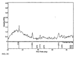
- FIGS. 2A-2C display the X-ray diffraction (XRD) ⁇ -2 ⁇ patterns of the titania films deposited on glass and silicon substrates under various conditions.
- the standard powder XRD pattern of rutile (from the Powder Diffraction File published by the International Center for Diffraction Data) is also indicated in the lower half of each figure.
- the XRD results of FIG. 2A and FIG. 2C are recorded with a Rigaku MiniFlex X-Ray Diffractometer.
- the XRD pattern in FIG. 2B is recorded with a Rigaku Rotoflex Diffractometer that has a higher X-ray intensity and a better signal to noise ratio on the diffraction patterns.
- FIG. 1 X-ray diffraction
- FIG. 2A shows the XRD result of the crystalline structure of a sample deposited on a glass substrate by ablating a titanium oxide target in vacuum with a laser fluence of 0.4 J/cm 2 .
- the X-ray diffraction pattern of the sample in FIG. 2A possess several diffraction peaks which correspond to the rutile phase.
- FIG. 2B shows the XRD result of the crystalline structure of a sample deposited on a single crystal silicon (100) substrate by ablating a titanium oxide target in vacuum with a laser fluence of 0.4 J/cm 2 .
- FIG. 2C shows the XRD result of the crystalline structure of a sample deposited on a glass substrate by ablating a titanium metal target under an oxygen pressure of 100 Pa with a laser fluence of 0.3 J/cm 2 not within the scope of protection.
- This XRD patterns also correspond to the rutile phase. This suggests that the ablated titanium metal reacts with oxygen to form titanium oxide. It is worth noting that only the rutile phase is exhibited in the above XRD results.
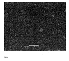
- FIG. 3 displays an SEM image of a film deposited on a silicon substrate by ablating a titanium oxide target under 0.1 Pa of oxygen. It is evident that this film is mostly composed of small particles with sizes less than one micrometer not within the scope of protection. The larger particles are aggregates of the smaller nanoparticles.
- the TEM image in FIG. 4 further confirms this observation, which shows the particle size is less than 100 nanometers. (The sample for FIG. 4 was deposited on a TEM grid by ablating a titanium metal target under an oxygen pressure of 100 Pa with a laser fluence of 0.4 J/cm 2 .)
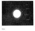
- FIG. 5A and 5B display the SAED patterns of two samples deposited on TEM grids.
- the SAED pattern in FIG. 5A can be indexed to the rutile structure.
- the SAED patterns in FIG. 5B show the coexistence of rutile and anatase phases.
- the lattice fringes in the high resolution TEM (HRTEM) image ( FIG. 5C ) are obtained by an electron beam aligned to the TiO 2 [001] direction
- the lattice fringes in the HRTEM image FIG. 5D
- the well parallel fringes indicate a single crystalline particle.
- the background gas is reactive, for example oxygen
- oxygen there are additional benefits that can help to bring in new chemical and structural properties.
- the ablated metal can react with oxygen to form metal oxide nanoparticles.
- nanoparticles with oxide shell and metal core structures can also be formed.
- a laser fluence in the range of about .2 J /cm2 to .6 J/cm2 provided good results.
- the fluence range is within the range .01 J/cm2 to 2 J/cm2.
Landscapes
- Chemical & Material Sciences (AREA)
- Organic Chemistry (AREA)
- Engineering & Computer Science (AREA)
- Materials Engineering (AREA)
- Metallurgy (AREA)
- Mechanical Engineering (AREA)
- Chemical Kinetics & Catalysis (AREA)
- Crystallography & Structural Chemistry (AREA)
- Health & Medical Sciences (AREA)
- Toxicology (AREA)
- Inorganic Chemistry (AREA)
- Physical Vapour Deposition (AREA)
- Inorganic Compounds Of Heavy Metals (AREA)
- Physical Deposition Of Substances That Are Components Of Semiconductor Devices (AREA)
Claims (17)
- Procédé pour déposer des nanoparticules ou des films nanocomposites d'oxyde métallique cristallin sur un substrat, ledit procédé comprenant :l'obtention d'une cible que comprend un matériau en oxyde métallique ;l'obtention d'un substrat pour soutenir les particules ou films d'oxyde métallique cristallin déposés ;l'ablation de régions de ladite cible avec des impulsions laser ultracourtes pour créer un panache de particules dirigées vers ledit substrat ; etle dépôt desdites nanoparticules ou desdits films nanocomposites sur ledit substrat,dans lequel le dépôt est effectué à une température de substrat inférieure à 300 °C,dans lequel la largeur des impulsions laser ultracourtes se situe dans la gamme de 10 fs à 100 ps et la fluence laser à la surface de ladite cible se situe dans la gamme de 0,01 J/cm2 à 2 J/cm2, etdans lequel les nanoparticules ou les films nanocomposites d'oxyde métallique cristallin sont des nanoparticules ou des films nanocomposites de TiO2 cristallin, et la cible comprend un matériau contenant du titane.
- Procédé selon la revendication 1, dans lequel les nanoparticules ont des tailles allant jusqu'à 1 µm.
- Procédé selon la revendication 1, dans lequel le faisceau laser a un profil « à sommet plat » pour obtenir une fluence uniforme sur la surface de la cible.
- Procédé selon la revendication 1, dans lequel la pression est de 100 Pa, 1 Pa ou 0,1 Pa.
- Procédé selon la revendication 1, dans lequel ladite température est la température ambiante et le dépôt est effectué sans aucun traitement thermique.
- Procédé selon la revendication 1, dans lequel lesdits films nanocomposites sont des films d'assemblage de nanoparticules de TiO2 cristallin.
- Procédé selon la revendication 1, dans lequel lesdits films nanocomposites sont composés d'un matériau hôte dans lequel sont incorporées des nanoparticules de TiO2 cristallin et dans lequel ledit matériau hôte est un oxyde de titane sous forme cristalline ou amorphe ou bien une céramique ou un polymère.
- Procédé selon la revendication 1, dans lequel ledit TiO2 cristallin se trouve dans une phase anatase, ou une phase rutile, ou une phase brookite, ou un mélange de deux quelconques ou des trois phases.
- Procédé selon la revendication 1, comprenant en outre l'étape d'obtention d'une chambre à vide contenant ladite cible et ledit substrat.
- Procédé selon la revendication 1 ou 9, dans lequel ledit dépôt est effectué sous vide ou dans un ou plusieurs gaz de fond contenant de l'oxygène.
- Procédé selon la revendication 10, dans lequel ledit dépôt est effectué à température ambiante.
- Procédé selon la revendication 1 ou 9, dans lequel ledit substrat comprend du verre, ou du papier, ou un plastique, ou un polymère.
- Procédé selon la revendication 9, dans lequel le laser à impulsions ultracourtes présente une fréquence de répétition de 1 kHz - 100 MHz.
- Procédé selon la revendication 9, dans lequel le système optique fait passer la distribution d'intensité du faisceau laser d'un profil gaussien à un profil « à sommet plat ».
- Procédé selon la revendication 1 ou 9, dans lequel ladite cible est un oxyde, ledit oxyde étant l'oxyde de titane.
- Procédé selon la revendication 1 ou 9, dans lequel ladite cible comprend de l'oxyde de titane et le dépôt sur ledit substrat a lieu sous vide ou dans un ou plusieurs gaz de fond contenant de l'oxygène.
- Procédé selon la revendication 1, dans lequel ledit substrat comprend du silicium, ledit matériau de cible comprend un oxyde de titane et ledit matériau de cible est décapé à une pression d'oxygène de 0,1 Pa, et les particules à l'intérieur dudit film cristallin présentent des tailles inférieures à 1 µm.
Priority Applications (1)
| Application Number | Priority Date | Filing Date | Title |
|---|---|---|---|
| EP13167101.8A EP2671970B1 (fr) | 2007-02-07 | 2008-01-31 | Procédé permettant de déposer des nanoparticules et des films de titane cristallin |
Applications Claiming Priority (3)
| Application Number | Priority Date | Filing Date | Title |
|---|---|---|---|
| US89989207P | 2007-02-07 | 2007-02-07 | |
| US11/798,114 US20080187684A1 (en) | 2007-02-07 | 2007-05-10 | Method for depositing crystalline titania nanoparticles and films |
| PCT/US2008/052544 WO2008118533A2 (fr) | 2007-02-07 | 2008-01-31 | Procédé pour déposer des nanoparticules et des films d'oxyde de titane cristallin |
Related Child Applications (2)
| Application Number | Title | Priority Date | Filing Date |
|---|---|---|---|
| EP13167101.8A Division EP2671970B1 (fr) | 2007-02-07 | 2008-01-31 | Procédé permettant de déposer des nanoparticules et des films de titane cristallin |
| EP13167101.8 Division-Into | 2013-05-08 |
Publications (3)
| Publication Number | Publication Date |
|---|---|
| EP2109694A2 EP2109694A2 (fr) | 2009-10-21 |
| EP2109694A4 EP2109694A4 (fr) | 2010-06-23 |
| EP2109694B1 true EP2109694B1 (fr) | 2013-06-26 |
Family
ID=39676397
Family Applications (2)
| Application Number | Title | Priority Date | Filing Date |
|---|---|---|---|
| EP08799669.0A Not-in-force EP2109694B1 (fr) | 2007-02-07 | 2008-01-31 | Procédé pour déposer des nanoparticules et des films d'oxyde de titane cristallin |
| EP13167101.8A Not-in-force EP2671970B1 (fr) | 2007-02-07 | 2008-01-31 | Procédé permettant de déposer des nanoparticules et des films de titane cristallin |
Family Applications After (1)
| Application Number | Title | Priority Date | Filing Date |
|---|---|---|---|
| EP13167101.8A Not-in-force EP2671970B1 (fr) | 2007-02-07 | 2008-01-31 | Procédé permettant de déposer des nanoparticules et des films de titane cristallin |
Country Status (5)
| Country | Link |
|---|---|
| US (3) | US20080187684A1 (fr) |
| EP (2) | EP2109694B1 (fr) |
| JP (2) | JP5468908B2 (fr) |
| CN (2) | CN103382546A (fr) |
| WO (1) | WO2008118533A2 (fr) |
Families Citing this family (49)
| Publication number | Priority date | Publication date | Assignee | Title |
|---|---|---|---|---|
| US20100221489A1 (en) * | 2006-02-23 | 2010-09-02 | Picodeon Ltd Oy | Coating on a glass substrate and a coated glass product |
| US20080006524A1 (en) * | 2006-07-05 | 2008-01-10 | Imra America, Inc. | Method for producing and depositing nanoparticles |
| US20080187684A1 (en) * | 2007-02-07 | 2008-08-07 | Imra America, Inc. | Method for depositing crystalline titania nanoparticles and films |
| US7767272B2 (en) * | 2007-05-25 | 2010-08-03 | Imra America, Inc. | Method of producing compound nanorods and thin films |
| CN101712468B (zh) * | 2008-09-30 | 2014-08-20 | 清华大学 | 碳纳米管复合材料及其制备方法 |
| CN104192792B (zh) * | 2008-11-14 | 2016-06-29 | 清华大学 | 纳米结构的制备方法 |
| US8663754B2 (en) | 2009-03-09 | 2014-03-04 | Imra America, Inc. | Pulsed laser micro-deposition pattern formation |
| CN101837287B (zh) * | 2009-03-21 | 2012-05-30 | 清华大学 | 碳纳米管纳米颗粒复合材料的制备方法 |
| CN101880023B (zh) * | 2009-05-08 | 2015-08-26 | 清华大学 | 纳米材料薄膜结构 |
| US20110133129A1 (en) * | 2009-12-07 | 2011-06-09 | Imra America, Inc. | Method of tuning properties of thin films |
| US20110192450A1 (en) * | 2010-02-10 | 2011-08-11 | Bing Liu | Method for producing nanoparticle solutions based on pulsed laser ablation for fabrication of thin film solar cells |
| US8540173B2 (en) * | 2010-02-10 | 2013-09-24 | Imra America, Inc. | Production of fine particles of functional ceramic by using pulsed laser |
| US8836941B2 (en) * | 2010-02-10 | 2014-09-16 | Imra America, Inc. | Method and apparatus to prepare a substrate for molecular detection |
| US9211611B2 (en) * | 2010-05-24 | 2015-12-15 | Purdue Research Foundation | Laser crystallization of thin films on various substrates at low temperatures |
| US8580226B2 (en) | 2010-10-29 | 2013-11-12 | Graver Technologies, Llc | Synthesis of sodium titanate and ion exchange use thereof |
| US8802234B2 (en) | 2011-01-03 | 2014-08-12 | Imra America, Inc. | Composite nanoparticles and methods for making the same |
| CN102134095B (zh) * | 2011-04-21 | 2012-12-26 | 浙江理工大学 | 一种制备核壳结构二氧化钛纳米颗粒的方法 |
| CN102372500A (zh) * | 2011-05-31 | 2012-03-14 | 安徽大学 | 激光脉冲沉积法制备Cu扩散掺杂ZnO基半导体的方法 |
| JP5983610B2 (ja) | 2011-08-08 | 2016-09-06 | 味の素株式会社 | 多孔質構造体及びその製造方法 |
| US8835285B2 (en) * | 2011-08-22 | 2014-09-16 | Flux Photon Corporation | Methods to fabricate vertically oriented anatase nanowire arrays on transparent conductive substrates and applications thereof |
| CN102615436A (zh) * | 2012-04-09 | 2012-08-01 | 镇江大成新能源有限公司 | 薄膜太阳能电池飞秒激光刻蚀工艺过程测控方法 |
| WO2014025743A1 (fr) | 2012-08-07 | 2014-02-13 | Cornell University | Composant à base de nanoparticules sans liant et sans carbone, procédé et applications |
| GB2509985A (en) * | 2013-01-22 | 2014-07-23 | M Solv Ltd | Method of forming patterns on coatings on opposite sides of a transparent substrate |
| US10283691B2 (en) | 2013-02-14 | 2019-05-07 | Dillard University | Nano-composite thermo-electric energy converter and fabrication method thereof |
| US9803284B2 (en) | 2013-05-10 | 2017-10-31 | 3M Innovative Properties Company | Method of depositing titania on a substrate and composite article |
| JP6283197B2 (ja) * | 2013-10-24 | 2018-02-21 | 独立行政法人国立高等専門学校機構 | 除菌、殺菌又は減菌装置及び除菌、殺菌又は減菌方法 |
| US9349535B2 (en) | 2013-12-17 | 2016-05-24 | Metastable Materials, Inc. | Method and apparatus for manufacturing isotropic magnetic nanocolloids by pulsed laser ablation |
| US10828400B2 (en) | 2014-06-10 | 2020-11-10 | The Research Foundation For The State University Of New York | Low temperature, nanostructured ceramic coatings |
| ES2558183B1 (es) * | 2014-07-01 | 2016-11-11 | Consejo Superior De Investigaciones Científicas (Csic) | Capa catalítica y su uso en membranas permeables al oxigeno |
| CN106148902A (zh) * | 2015-04-14 | 2016-11-23 | 天津职业技术师范大学 | 一种均匀较厚介孔氧化钛纳米颗粒薄膜的飞秒激光制备方法 |
| CN104988507A (zh) * | 2015-05-28 | 2015-10-21 | 湖北工业大学 | 一种利用超快激光制备铸铁超疏水耐腐蚀表面的方法 |
| JP6681683B2 (ja) * | 2015-08-27 | 2020-04-15 | 日本電気硝子株式会社 | 光学膜及びその製造方法 |
| CN105363427A (zh) * | 2015-12-01 | 2016-03-02 | 中国科学院长春光学精密机械与物理研究所 | 具有可见光催化活性的TiO2纳米材料、应用及其制备方法 |
| US10316403B2 (en) | 2016-02-17 | 2019-06-11 | Dillard University | Method for open-air pulsed laser deposition |
| JP6670497B2 (ja) * | 2016-03-02 | 2020-03-25 | 国立大学法人京都工芸繊維大学 | 結晶膜および非結晶薄膜の製造方法および製造装置 |
| CN105803404A (zh) * | 2016-03-25 | 2016-07-27 | 武汉华星光电技术有限公司 | 薄膜沉积组件及薄膜沉积装置 |
| CN106624369A (zh) * | 2016-10-14 | 2017-05-10 | 清华大学 | 一种快速制备氧化物多级纳米结构的方法 |
| CN107271488B (zh) * | 2017-06-15 | 2019-12-27 | 电子科技大学 | 一种纳米复合结构气敏材料的制备方法 |
| CN109487219A (zh) * | 2018-07-24 | 2019-03-19 | 深圳市矩阵多元科技有限公司 | 脉冲激光沉积系统及其薄膜制备方法 |
| CN109238974A (zh) * | 2018-08-30 | 2019-01-18 | 南京理工大学 | 一种日盲型深紫外等离子体共振纳米颗粒的制备方法 |
| CN111482173B (zh) * | 2019-01-25 | 2022-08-16 | 华中师范大学 | CuO/板钛矿型TiO2的复合纳米材料及其应用 |
| CN110230084B (zh) * | 2019-04-15 | 2020-09-11 | 清华大学 | 基于飞秒激光退火处理的钛表面多晶结构形成方法及系统 |
| AU2020290956A1 (en) * | 2019-06-12 | 2022-01-06 | Auburn University | Novel additive nanomanufacturing system and method |
| CN111850653B (zh) * | 2020-06-23 | 2021-07-06 | 清华大学 | 利用飞秒激光制备暴露高活性面的二氧化钛的方法及系统 |
| EP3943197A1 (fr) | 2020-07-20 | 2022-01-26 | The Provost, Fellows, Scholars and other Members of Board of Trinity College Dublin | Dépôt par jet à l'aide d'un aérosol sec produit par laser |
| CN113463045B (zh) * | 2021-06-11 | 2022-10-14 | 华中科技大学 | 一种激光脉冲沉积系统及加工方法 |
| EP4314375A1 (fr) * | 2021-07-01 | 2024-02-07 | Max-Planck-Gesellschaft zur Förderung der Wissenschaften e.V. | Procédé de formation d'une couche d'un composé |
| CN115537737B (zh) * | 2022-10-13 | 2023-11-17 | 西南交通大学 | 一种薄涂层的制备方法及系统 |
| CN115988941B (zh) * | 2022-12-13 | 2025-06-27 | 湖北万度光能有限责任公司 | 一种激光烧结钙钛矿太阳能电池及其制备方法 |
Family Cites Families (41)
| Publication number | Priority date | Publication date | Assignee | Title |
|---|---|---|---|---|
| CA1196617A (fr) | 1982-07-14 | 1985-11-12 | George E. Morris | Lit de catalyse, sa preparation et son emploi en production d'hydrocarbures a partir de gaz de synthese |
| US4932747A (en) * | 1989-09-07 | 1990-06-12 | The United States Of America As Represented By The Secretary Of The Navy | Fiber bundle homogenizer and method utilizing same |
| US5338625A (en) * | 1992-07-29 | 1994-08-16 | Martin Marietta Energy Systems, Inc. | Thin film battery and method for making same |
| US5432151A (en) * | 1993-07-12 | 1995-07-11 | Regents Of The University Of California | Process for ion-assisted laser deposition of biaxially textured layer on substrate |
| US5656186A (en) * | 1994-04-08 | 1997-08-12 | The Regents Of The University Of Michigan | Method for controlling configuration of laser induced breakdown and ablation |
| US5490912A (en) * | 1994-05-31 | 1996-02-13 | The Regents Of The University Of California | Apparatus for laser assisted thin film deposition |
| AUPO912797A0 (en) | 1997-09-11 | 1997-10-02 | Australian National University, The | Ultrafast laser deposition method |
| JP2000100457A (ja) * | 1998-09-25 | 2000-04-07 | Matsushita Electric Ind Co Ltd | 燃料電池 |
| AU6431199A (en) * | 1998-10-12 | 2000-05-01 | Regents Of The University Of California, The | Laser deposition of thin films |
| US6274207B1 (en) * | 1999-05-21 | 2001-08-14 | The Board Of Regents, The University Of Texas System | Method of coating three dimensional objects with molecular sieves |
| WO2001073883A2 (fr) * | 2000-03-24 | 2001-10-04 | Cymbet Corporation | Fabrication basse temperature de dispositifs d'accumulation d'energie en couche mince |
| US6645656B1 (en) * | 2000-03-24 | 2003-11-11 | University Of Houston | Thin film solid oxide fuel cell and method for forming |
| JP4747330B2 (ja) | 2000-07-03 | 2011-08-17 | 独立行政法人 日本原子力研究開発機構 | ルチル型酸化チタン単結晶薄膜の作製法 |
| JP3550658B2 (ja) | 2000-12-28 | 2004-08-04 | 独立行政法人産業技術総合研究所 | 結晶構造の制御された二酸化チタン系薄膜の製造方法 |
| US20050034668A1 (en) * | 2001-03-22 | 2005-02-17 | Garvey James F. | Multi-component substances and apparatus for preparation thereof |
| CA2442985C (fr) * | 2001-03-30 | 2016-05-31 | The Regents Of The University Of California | Procede de realisation de nanostructures et de nanocables, et dispositifs etablis a partir de ce type d'equipement |
| FR2824846B1 (fr) * | 2001-05-16 | 2004-04-02 | Saint Gobain | Substrat a revetement photocatalytique |
| JP3735686B2 (ja) | 2001-10-30 | 2006-01-18 | 独立行政法人理化学研究所 | 金属酸化物強誘電体粒子結晶の製造方法 |
| DE10153640A1 (de) * | 2001-10-31 | 2003-05-15 | Inst Neue Mat Gemein Gmbh | Beschichtete Titandioxid-Teilchen |
| US6713987B2 (en) * | 2002-02-28 | 2004-03-30 | Front Edge Technology, Inc. | Rechargeable battery having permeable anode current collector |
| JP2003306319A (ja) | 2002-04-10 | 2003-10-28 | Japan Atom Energy Res Inst | 金属酸化物ナノ微粒子の製造方法 |
| US6884739B2 (en) * | 2002-08-15 | 2005-04-26 | Micron Technology Inc. | Lanthanide doped TiOx dielectric films by plasma oxidation |
| AU2003301770A1 (en) * | 2002-08-16 | 2004-06-07 | The Regents Of The University Of California | Functional bimorph composite nanotapes and methods of fabrication |
| JP2004107150A (ja) * | 2002-09-19 | 2004-04-08 | Satasu:Kk | ガラスマーキング方法 |
| JP2004195339A (ja) * | 2002-12-17 | 2004-07-15 | Matsushita Electric Ind Co Ltd | ナノ構造体の形成方法並びにナノ構造体 |
| JP4224850B2 (ja) | 2003-02-25 | 2009-02-18 | 独立行政法人 日本原子力研究開発機構 | 光触媒アナターゼ型二酸化チタン薄膜の製造方法 |
| FI118516B (fi) | 2003-03-14 | 2007-12-14 | Neste Oil Oyj | Menetelmä katalyytin valmistamiseksi |
| US7179508B2 (en) * | 2003-05-30 | 2007-02-20 | The Board Of Trustees Of The University Of Illinois | Conducting polymer films and method of manufacturing the same by surface polymerization using ion-assisted deposition |
| KR100682886B1 (ko) * | 2003-12-18 | 2007-02-15 | 삼성전자주식회사 | 나노입자의 제조방법 |
| US7491909B2 (en) * | 2004-03-31 | 2009-02-17 | Imra America, Inc. | Pulsed laser processing with controlled thermal and physical alterations |
| US7486705B2 (en) * | 2004-03-31 | 2009-02-03 | Imra America, Inc. | Femtosecond laser processing system with process parameters, controls and feedback |
| CA2560984A1 (fr) | 2004-06-01 | 2005-12-15 | Teva Gyogyszergyar Zartkoruen Mukodo Reszvenytarsasag | Procedure de preparation d'un medicament de forme amorphe |
| WO2005118546A1 (fr) | 2004-06-04 | 2005-12-15 | Matrix Laboratories Ltd | Nouvelles formes cristallines de gatifloxacine |
| US7879410B2 (en) * | 2004-06-09 | 2011-02-01 | Imra America, Inc. | Method of fabricating an electrochemical device using ultrafast pulsed laser deposition |
| JP2006019479A (ja) * | 2004-07-01 | 2006-01-19 | Fuji Photo Film Co Ltd | 光電変換要素、その製造方法、カラーセンサー及びカラー撮像システム |
| US20060039419A1 (en) * | 2004-08-16 | 2006-02-23 | Tan Deshi | Method and apparatus for laser trimming of resistors using ultrafast laser pulse from ultrafast laser oscillator operating in picosecond and femtosecond pulse widths |
| KR100707172B1 (ko) * | 2004-09-04 | 2007-04-13 | 삼성전자주식회사 | 레이저 어블레이션 장치 및 이를 이용한 나노입자의제조방법 |
| WO2006090004A1 (fr) * | 2005-02-23 | 2006-08-31 | Picodeon Ltd Oy | Procede de depot au laser a impulsion |
| AU2006264650B2 (en) | 2005-07-01 | 2012-08-23 | Generics [Uk] Limited | Zofenopril calcium in polymorph form C |
| US20080006524A1 (en) * | 2006-07-05 | 2008-01-10 | Imra America, Inc. | Method for producing and depositing nanoparticles |
| US20080187684A1 (en) | 2007-02-07 | 2008-08-07 | Imra America, Inc. | Method for depositing crystalline titania nanoparticles and films |
-
2007
- 2007-05-10 US US11/798,114 patent/US20080187684A1/en not_active Abandoned
-
2008
- 2008-01-31 WO PCT/US2008/052544 patent/WO2008118533A2/fr not_active Ceased
- 2008-01-31 JP JP2009549175A patent/JP5468908B2/ja not_active Expired - Fee Related
- 2008-01-31 EP EP08799669.0A patent/EP2109694B1/fr not_active Not-in-force
- 2008-01-31 CN CN2013102382858A patent/CN103382546A/zh active Pending
- 2008-01-31 CN CN2008800018135A patent/CN101589173B/zh not_active Expired - Fee Related
- 2008-01-31 EP EP13167101.8A patent/EP2671970B1/fr not_active Not-in-force
-
2009
- 2009-07-02 US US12/497,205 patent/US8609205B2/en not_active Expired - Fee Related
-
2013
- 2013-08-15 JP JP2013168848A patent/JP5784081B2/ja not_active Expired - Fee Related
- 2013-12-05 US US14/097,633 patent/US20140093744A1/en not_active Abandoned
Also Published As
| Publication number | Publication date |
|---|---|
| JP2014012897A (ja) | 2014-01-23 |
| US20090311513A1 (en) | 2009-12-17 |
| WO2008118533A3 (fr) | 2008-11-20 |
| CN103382546A (zh) | 2013-11-06 |
| US20080187684A1 (en) | 2008-08-07 |
| EP2109694A2 (fr) | 2009-10-21 |
| EP2109694A4 (fr) | 2010-06-23 |
| CN101589173A (zh) | 2009-11-25 |
| JP5784081B2 (ja) | 2015-09-24 |
| US20140093744A1 (en) | 2014-04-03 |
| CN101589173B (zh) | 2013-07-24 |
| WO2008118533A2 (fr) | 2008-10-02 |
| JP2010518257A (ja) | 2010-05-27 |
| US8609205B2 (en) | 2013-12-17 |
| EP2671970B1 (fr) | 2014-07-23 |
| EP2671970A1 (fr) | 2013-12-11 |
| JP5468908B2 (ja) | 2014-04-09 |
Similar Documents
| Publication | Publication Date | Title |
|---|---|---|
| EP2109694B1 (fr) | Procédé pour déposer des nanoparticules et des films d'oxyde de titane cristallin | |
| Haider et al. | A comprehensive review on pulsed laser deposition technique to effective nanostructure production: Trends and challenges | |
| Chen et al. | Fabricating highly active mixed phase TiO2 photocatalysts by reactive DC magnetron sputter deposition | |
| Singh et al. | Room temperature growth of nanocrystalline anatase TiO2 thin films by dc magnetron sputtering | |
| CN104649233B (zh) | 一种金属氧化物纳米线的可控图案化超快激光复合制备方法 | |
| Henkel et al. | Self-organized nanocrack networks: a pathway to enlarge catalytic surface area in sputtered ceramic thin films, showcased for photocatalytic TiO2 | |
| Choi et al. | Fabrication and characterization of anatase TiO2 thin film on glass substrate grown by pulsed laser deposition | |
| Shafeeq et al. | Niobium Pentoxide Nanostructures Fabricated by the Fundamental Q-Switched Nd: YAG PLD under Vacuum Conditions. | |
| Chen et al. | Production of amorphous tin oxide thin films and microstructural transformation induced by heat treatment | |
| Vasconcelos et al. | TiO2 Nanocoatings on Natural Fibers by DC Reactive Magnetron | |
| Al-Obaidi et al. | Synthesis of nanostructured TiO2 thin films by pulsed laser deposition (PLD) and the effect of annealing temperature on structural and morphological properties | |
| US7763113B2 (en) | Photocatalyst material and method for preparation thereof | |
| Chen et al. | Photocatalytic TiO2 thin films deposited on flexible substrates by radio frequency (RF) reactive magnetron sputtering | |
| Yasuda et al. | Low-temperature deposition of crystallized TiO2 thin films | |
| Bočkutė et al. | The investigation of E-beam deposited titanium dioxide and calcium titanate thin films | |
| CN101139702B (zh) | 脉冲激光沉积制备硅基锐钛矿相TiO2薄膜的方法 | |
| Srivatsa et al. | Synthesis of anatase titania nanostructures at room temperature by PECVD technique | |
| Kavei et al. | Equilibrium state of anatase to rutile transformation for titanium dioxide film prepared by ultrasonic spray pyrolysis technique | |
| Wang et al. | Photocatalytic performance of TiO2 thin films deposited on soda-lime glass and the effect of post-annealing on their properties | |
| Deng et al. | Comparison of vanadium oxide thin films prepared using femtosecond and nanosecond pulsed laser deposition | |
| Mansur et al. | Sputtering technique | |
| JP3355372B2 (ja) | レーザーによる薄膜形成方法 | |
| Xu et al. | Anatase TiO2 films fabricated by pulsed laser deposition using Ti target | |
| CN116445875B (zh) | 一种超疏水氧化铈膜及其制备方法 | |
| Tveryanovich et al. | Production of nanodispersed materials and thin films by laser ablation techniques in liquid and in vacuum |
Legal Events
| Date | Code | Title | Description |
|---|---|---|---|
| PUAI | Public reference made under article 153(3) epc to a published international application that has entered the european phase |
Free format text: ORIGINAL CODE: 0009012 |
|
| 17P | Request for examination filed |
Effective date: 20090807 |
|
| AK | Designated contracting states |
Kind code of ref document: A2 Designated state(s): AT BE BG CH CY CZ DE DK EE ES FI FR GB GR HR HU IE IS IT LI LT LU LV MC MT NL NO PL PT RO SE SI SK TR |
|
| RIN1 | Information on inventor provided before grant (corrected) |
Inventor name: CHE, YONG Inventor name: HU, ZHENDONG Inventor name: LIU, BING |
|
| RIC1 | Information provided on ipc code assigned before grant |
Ipc: C23C 20/04 20060101AFI20090818BHEP Ipc: C23C 20/02 20060101ALI20100511BHEP |
|
| A4 | Supplementary search report drawn up and despatched |
Effective date: 20100526 |
|
| 17Q | First examination report despatched |
Effective date: 20120124 |
|
| DAX | Request for extension of the european patent (deleted) | ||
| GRAP | Despatch of communication of intention to grant a patent |
Free format text: ORIGINAL CODE: EPIDOSNIGR1 |
|
| GRAS | Grant fee paid |
Free format text: ORIGINAL CODE: EPIDOSNIGR3 |
|
| GRAA | (expected) grant |
Free format text: ORIGINAL CODE: 0009210 |
|
| AK | Designated contracting states |
Kind code of ref document: B1 Designated state(s): AT BE BG CH CY CZ DE DK EE ES FI FR GB GR HR HU IE IS IT LI LT LU LV MC MT NL NO PL PT RO SE SI SK TR |
|
| REG | Reference to a national code |
Ref country code: GB Ref legal event code: FG4D |
|
| RIN1 | Information on inventor provided before grant (corrected) |
Inventor name: LIU, BING Inventor name: CHE, YONG Inventor name: HU, ZHENDONG |
|
| REG | Reference to a national code |
Ref country code: CH Ref legal event code: EP |
|
| REG | Reference to a national code |
Ref country code: AT Ref legal event code: REF Ref document number: 618750 Country of ref document: AT Kind code of ref document: T Effective date: 20130715 |
|
| REG | Reference to a national code |
Ref country code: IE Ref legal event code: FG4D |
|
| REG | Reference to a national code |
Ref country code: DE Ref legal event code: R096 Ref document number: 602008025611 Country of ref document: DE Effective date: 20130822 |
|
| PG25 | Lapsed in a contracting state [announced via postgrant information from national office to epo] |
Ref country code: SI Free format text: LAPSE BECAUSE OF FAILURE TO SUBMIT A TRANSLATION OF THE DESCRIPTION OR TO PAY THE FEE WITHIN THE PRESCRIBED TIME-LIMIT Effective date: 20130626 Ref country code: FI Free format text: LAPSE BECAUSE OF FAILURE TO SUBMIT A TRANSLATION OF THE DESCRIPTION OR TO PAY THE FEE WITHIN THE PRESCRIBED TIME-LIMIT Effective date: 20130626 Ref country code: NO Free format text: LAPSE BECAUSE OF FAILURE TO SUBMIT A TRANSLATION OF THE DESCRIPTION OR TO PAY THE FEE WITHIN THE PRESCRIBED TIME-LIMIT Effective date: 20130926 Ref country code: LT Free format text: LAPSE BECAUSE OF FAILURE TO SUBMIT A TRANSLATION OF THE DESCRIPTION OR TO PAY THE FEE WITHIN THE PRESCRIBED TIME-LIMIT Effective date: 20130626 Ref country code: SE Free format text: LAPSE BECAUSE OF FAILURE TO SUBMIT A TRANSLATION OF THE DESCRIPTION OR TO PAY THE FEE WITHIN THE PRESCRIBED TIME-LIMIT Effective date: 20130626 Ref country code: GR Free format text: LAPSE BECAUSE OF FAILURE TO SUBMIT A TRANSLATION OF THE DESCRIPTION OR TO PAY THE FEE WITHIN THE PRESCRIBED TIME-LIMIT Effective date: 20130927 |
|
| REG | Reference to a national code |
Ref country code: AT Ref legal event code: MK05 Ref document number: 618750 Country of ref document: AT Kind code of ref document: T Effective date: 20130626 |
|
| REG | Reference to a national code |
Ref country code: LT Ref legal event code: MG4D |
|
| PG25 | Lapsed in a contracting state [announced via postgrant information from national office to epo] |
Ref country code: BG Free format text: LAPSE BECAUSE OF FAILURE TO SUBMIT A TRANSLATION OF THE DESCRIPTION OR TO PAY THE FEE WITHIN THE PRESCRIBED TIME-LIMIT Effective date: 20130926 Ref country code: HR Free format text: LAPSE BECAUSE OF FAILURE TO SUBMIT A TRANSLATION OF THE DESCRIPTION OR TO PAY THE FEE WITHIN THE PRESCRIBED TIME-LIMIT Effective date: 20130626 |
|
| REG | Reference to a national code |
Ref country code: NL Ref legal event code: VDEP Effective date: 20130626 |
|
| PG25 | Lapsed in a contracting state [announced via postgrant information from national office to epo] |
Ref country code: LV Free format text: LAPSE BECAUSE OF FAILURE TO SUBMIT A TRANSLATION OF THE DESCRIPTION OR TO PAY THE FEE WITHIN THE PRESCRIBED TIME-LIMIT Effective date: 20130626 |
|
| PG25 | Lapsed in a contracting state [announced via postgrant information from national office to epo] |
Ref country code: BE Free format text: LAPSE BECAUSE OF FAILURE TO SUBMIT A TRANSLATION OF THE DESCRIPTION OR TO PAY THE FEE WITHIN THE PRESCRIBED TIME-LIMIT Effective date: 20130626 Ref country code: CY Free format text: LAPSE BECAUSE OF FAILURE TO SUBMIT A TRANSLATION OF THE DESCRIPTION OR TO PAY THE FEE WITHIN THE PRESCRIBED TIME-LIMIT Effective date: 20130807 Ref country code: IS Free format text: LAPSE BECAUSE OF FAILURE TO SUBMIT A TRANSLATION OF THE DESCRIPTION OR TO PAY THE FEE WITHIN THE PRESCRIBED TIME-LIMIT Effective date: 20131026 Ref country code: CZ Free format text: LAPSE BECAUSE OF FAILURE TO SUBMIT A TRANSLATION OF THE DESCRIPTION OR TO PAY THE FEE WITHIN THE PRESCRIBED TIME-LIMIT Effective date: 20130626 Ref country code: PT Free format text: LAPSE BECAUSE OF FAILURE TO SUBMIT A TRANSLATION OF THE DESCRIPTION OR TO PAY THE FEE WITHIN THE PRESCRIBED TIME-LIMIT Effective date: 20131028 Ref country code: AT Free format text: LAPSE BECAUSE OF FAILURE TO SUBMIT A TRANSLATION OF THE DESCRIPTION OR TO PAY THE FEE WITHIN THE PRESCRIBED TIME-LIMIT Effective date: 20130626 Ref country code: SK Free format text: LAPSE BECAUSE OF FAILURE TO SUBMIT A TRANSLATION OF THE DESCRIPTION OR TO PAY THE FEE WITHIN THE PRESCRIBED TIME-LIMIT Effective date: 20130626 Ref country code: EE Free format text: LAPSE BECAUSE OF FAILURE TO SUBMIT A TRANSLATION OF THE DESCRIPTION OR TO PAY THE FEE WITHIN THE PRESCRIBED TIME-LIMIT Effective date: 20130626 |
|
| PG25 | Lapsed in a contracting state [announced via postgrant information from national office to epo] |
Ref country code: RO Free format text: LAPSE BECAUSE OF FAILURE TO SUBMIT A TRANSLATION OF THE DESCRIPTION OR TO PAY THE FEE WITHIN THE PRESCRIBED TIME-LIMIT Effective date: 20130626 Ref country code: ES Free format text: LAPSE BECAUSE OF FAILURE TO SUBMIT A TRANSLATION OF THE DESCRIPTION OR TO PAY THE FEE WITHIN THE PRESCRIBED TIME-LIMIT Effective date: 20131007 Ref country code: PL Free format text: LAPSE BECAUSE OF FAILURE TO SUBMIT A TRANSLATION OF THE DESCRIPTION OR TO PAY THE FEE WITHIN THE PRESCRIBED TIME-LIMIT Effective date: 20130626 Ref country code: NL Free format text: LAPSE BECAUSE OF FAILURE TO SUBMIT A TRANSLATION OF THE DESCRIPTION OR TO PAY THE FEE WITHIN THE PRESCRIBED TIME-LIMIT Effective date: 20130626 |
|
| PG25 | Lapsed in a contracting state [announced via postgrant information from national office to epo] |
Ref country code: CY Free format text: LAPSE BECAUSE OF FAILURE TO SUBMIT A TRANSLATION OF THE DESCRIPTION OR TO PAY THE FEE WITHIN THE PRESCRIBED TIME-LIMIT Effective date: 20130626 |
|
| PG25 | Lapsed in a contracting state [announced via postgrant information from national office to epo] |
Ref country code: DK Free format text: LAPSE BECAUSE OF FAILURE TO SUBMIT A TRANSLATION OF THE DESCRIPTION OR TO PAY THE FEE WITHIN THE PRESCRIBED TIME-LIMIT Effective date: 20130626 |
|
| PLBE | No opposition filed within time limit |
Free format text: ORIGINAL CODE: 0009261 |
|
| STAA | Information on the status of an ep patent application or granted ep patent |
Free format text: STATUS: NO OPPOSITION FILED WITHIN TIME LIMIT |
|
| PG25 | Lapsed in a contracting state [announced via postgrant information from national office to epo] |
Ref country code: IT Free format text: LAPSE BECAUSE OF FAILURE TO SUBMIT A TRANSLATION OF THE DESCRIPTION OR TO PAY THE FEE WITHIN THE PRESCRIBED TIME-LIMIT Effective date: 20130626 |
|
| PGFP | Annual fee paid to national office [announced via postgrant information from national office to epo] |
Ref country code: FR Payment date: 20140108 Year of fee payment: 7 |
|
| 26N | No opposition filed |
Effective date: 20140327 |
|
| PGFP | Annual fee paid to national office [announced via postgrant information from national office to epo] |
Ref country code: GB Payment date: 20140129 Year of fee payment: 7 |
|
| REG | Reference to a national code |
Ref country code: DE Ref legal event code: R097 Ref document number: 602008025611 Country of ref document: DE Effective date: 20140327 |
|
| PG25 | Lapsed in a contracting state [announced via postgrant information from national office to epo] |
Ref country code: MC Free format text: LAPSE BECAUSE OF FAILURE TO SUBMIT A TRANSLATION OF THE DESCRIPTION OR TO PAY THE FEE WITHIN THE PRESCRIBED TIME-LIMIT Effective date: 20130626 Ref country code: LU Free format text: LAPSE BECAUSE OF FAILURE TO SUBMIT A TRANSLATION OF THE DESCRIPTION OR TO PAY THE FEE WITHIN THE PRESCRIBED TIME-LIMIT Effective date: 20140131 |
|
| REG | Reference to a national code |
Ref country code: CH Ref legal event code: PL |
|
| PG25 | Lapsed in a contracting state [announced via postgrant information from national office to epo] |
Ref country code: LI Free format text: LAPSE BECAUSE OF NON-PAYMENT OF DUE FEES Effective date: 20140131 Ref country code: CH Free format text: LAPSE BECAUSE OF NON-PAYMENT OF DUE FEES Effective date: 20140131 |
|
| REG | Reference to a national code |
Ref country code: IE Ref legal event code: MM4A |
|
| PG25 | Lapsed in a contracting state [announced via postgrant information from national office to epo] |
Ref country code: IE Free format text: LAPSE BECAUSE OF NON-PAYMENT OF DUE FEES Effective date: 20140131 |
|
| GBPC | Gb: european patent ceased through non-payment of renewal fee |
Effective date: 20150131 |
|
| PG25 | Lapsed in a contracting state [announced via postgrant information from national office to epo] |
Ref country code: GB Free format text: LAPSE BECAUSE OF NON-PAYMENT OF DUE FEES Effective date: 20150131 |
|
| REG | Reference to a national code |
Ref country code: FR Ref legal event code: ST Effective date: 20150930 |
|
| PG25 | Lapsed in a contracting state [announced via postgrant information from national office to epo] |
Ref country code: FR Free format text: LAPSE BECAUSE OF NON-PAYMENT OF DUE FEES Effective date: 20150202 |
|
| PG25 | Lapsed in a contracting state [announced via postgrant information from national office to epo] |
Ref country code: MT Free format text: LAPSE BECAUSE OF FAILURE TO SUBMIT A TRANSLATION OF THE DESCRIPTION OR TO PAY THE FEE WITHIN THE PRESCRIBED TIME-LIMIT Effective date: 20130626 |
|
| PGFP | Annual fee paid to national office [announced via postgrant information from national office to epo] |
Ref country code: DE Payment date: 20160127 Year of fee payment: 9 |
|
| PG25 | Lapsed in a contracting state [announced via postgrant information from national office to epo] |
Ref country code: HU Free format text: LAPSE BECAUSE OF FAILURE TO SUBMIT A TRANSLATION OF THE DESCRIPTION OR TO PAY THE FEE WITHIN THE PRESCRIBED TIME-LIMIT; INVALID AB INITIO Effective date: 20080131 Ref country code: TR Free format text: LAPSE BECAUSE OF FAILURE TO SUBMIT A TRANSLATION OF THE DESCRIPTION OR TO PAY THE FEE WITHIN THE PRESCRIBED TIME-LIMIT Effective date: 20130626 |
|
| REG | Reference to a national code |
Ref country code: DE Ref legal event code: R119 Ref document number: 602008025611 Country of ref document: DE |
|
| PG25 | Lapsed in a contracting state [announced via postgrant information from national office to epo] |
Ref country code: DE Free format text: LAPSE BECAUSE OF NON-PAYMENT OF DUE FEES Effective date: 20170801 |