EP2117000A1 - Support d'enregistrement d'informations - Google Patents
Support d'enregistrement d'informations Download PDFInfo
- Publication number
- EP2117000A1 EP2117000A1 EP09009028A EP09009028A EP2117000A1 EP 2117000 A1 EP2117000 A1 EP 2117000A1 EP 09009028 A EP09009028 A EP 09009028A EP 09009028 A EP09009028 A EP 09009028A EP 2117000 A1 EP2117000 A1 EP 2117000A1
- Authority
- EP
- European Patent Office
- Prior art keywords
- frequency
- shift modulation
- data
- recording
- address
- Prior art date
- Legal status (The legal status is an assumption and is not a legal conclusion. Google has not performed a legal analysis and makes no representation as to the accuracy of the status listed.)
- Granted
Links
- 239000010410 layer Substances 0.000 description 98
- 238000000034 method Methods 0.000 description 42
- 230000005540 biological transmission Effects 0.000 description 38
- 239000000463 material Substances 0.000 description 24
- 229920005989 resin Polymers 0.000 description 18
- 239000011347 resin Substances 0.000 description 18
- 238000010586 diagram Methods 0.000 description 17
- 239000000049 pigment Substances 0.000 description 12
- 229910045601 alloy Inorganic materials 0.000 description 9
- 239000000956 alloy Substances 0.000 description 9
- 230000003287 optical effect Effects 0.000 description 9
- 230000010363 phase shift Effects 0.000 description 9
- 230000008859 change Effects 0.000 description 8
- 238000001514 detection method Methods 0.000 description 8
- KDLHZDBZIXYQEI-UHFFFAOYSA-N Palladium Chemical compound [Pd] KDLHZDBZIXYQEI-UHFFFAOYSA-N 0.000 description 7
- BASFCYQUMIYNBI-UHFFFAOYSA-N platinum Chemical compound [Pt] BASFCYQUMIYNBI-UHFFFAOYSA-N 0.000 description 6
- 229910002601 GaN Inorganic materials 0.000 description 5
- JMASRVWKEDWRBT-UHFFFAOYSA-N Gallium nitride Chemical compound [Ga]#N JMASRVWKEDWRBT-UHFFFAOYSA-N 0.000 description 5
- 230000000694 effects Effects 0.000 description 5
- 230000001360 synchronised effect Effects 0.000 description 5
- 229910000763 AgInSbTe Inorganic materials 0.000 description 4
- KRHYYFGTRYWZRS-UHFFFAOYSA-M Fluoride anion Chemical compound [F-] KRHYYFGTRYWZRS-UHFFFAOYSA-M 0.000 description 4
- 239000004793 Polystyrene Substances 0.000 description 4
- UCKMPCXJQFINFW-UHFFFAOYSA-N Sulphide Chemical compound [S-2] UCKMPCXJQFINFW-UHFFFAOYSA-N 0.000 description 4
- 229910052782 aluminium Inorganic materials 0.000 description 4
- XAGFODPZIPBFFR-UHFFFAOYSA-N aluminium Chemical compound [Al] XAGFODPZIPBFFR-UHFFFAOYSA-N 0.000 description 4
- 239000000919 ceramic Substances 0.000 description 4
- 239000006185 dispersion Substances 0.000 description 4
- 238000010894 electron beam technology Methods 0.000 description 4
- 238000005516 engineering process Methods 0.000 description 4
- XEEYBQQBJWHFJM-UHFFFAOYSA-N iron Substances [Fe] XEEYBQQBJWHFJM-UHFFFAOYSA-N 0.000 description 4
- 229910052751 metal Inorganic materials 0.000 description 4
- 239000002184 metal Substances 0.000 description 4
- 230000004048 modification Effects 0.000 description 4
- 238000012986 modification Methods 0.000 description 4
- 150000004767 nitrides Chemical class 0.000 description 4
- 229910052763 palladium Inorganic materials 0.000 description 4
- 230000002093 peripheral effect Effects 0.000 description 4
- 229910052697 platinum Inorganic materials 0.000 description 4
- 239000004417 polycarbonate Substances 0.000 description 4
- 229920000515 polycarbonate Polymers 0.000 description 4
- 229920001296 polysiloxane Polymers 0.000 description 4
- 229920002223 polystyrene Polymers 0.000 description 4
- 239000000057 synthetic resin Substances 0.000 description 4
- 229920003002 synthetic resin Polymers 0.000 description 4
- 238000012360 testing method Methods 0.000 description 4
- 229910052718 tin Inorganic materials 0.000 description 4
- 229910000618 GeSbTe Inorganic materials 0.000 description 3
- 230000008901 benefit Effects 0.000 description 3
- 229910052797 bismuth Inorganic materials 0.000 description 3
- 239000002131 composite material Substances 0.000 description 3
- 239000010408 film Substances 0.000 description 3
- 229910052732 germanium Inorganic materials 0.000 description 3
- 239000011521 glass Substances 0.000 description 3
- 229910052742 iron Inorganic materials 0.000 description 3
- 238000005461 lubrication Methods 0.000 description 3
- 239000002365 multiple layer Substances 0.000 description 3
- 239000012782 phase change material Substances 0.000 description 3
- 238000002203 pretreatment Methods 0.000 description 3
- 238000002310 reflectometry Methods 0.000 description 3
- 239000004065 semiconductor Substances 0.000 description 3
- 239000004634 thermosetting polymer Substances 0.000 description 3
- VYZAMTAEIAYCRO-UHFFFAOYSA-N Chromium Chemical compound [Cr] VYZAMTAEIAYCRO-UHFFFAOYSA-N 0.000 description 2
- BQCADISMDOOEFD-UHFFFAOYSA-N Silver Chemical compound [Ag] BQCADISMDOOEFD-UHFFFAOYSA-N 0.000 description 2
- CDBYLPFSWZWCQE-UHFFFAOYSA-L Sodium Carbonate Chemical compound [Na+].[Na+].[O-]C([O-])=O CDBYLPFSWZWCQE-UHFFFAOYSA-L 0.000 description 2
- ATJFFYVFTNAWJD-UHFFFAOYSA-N Tin Chemical compound [Sn] ATJFFYVFTNAWJD-UHFFFAOYSA-N 0.000 description 2
- DZBUGLKDJFMEHC-UHFFFAOYSA-N acridine Chemical compound C1=CC=CC2=CC3=CC=CC=C3N=C21 DZBUGLKDJFMEHC-UHFFFAOYSA-N 0.000 description 2
- 125000002723 alicyclic group Chemical group 0.000 description 2
- 239000005354 aluminosilicate glass Substances 0.000 description 2
- 229910052785 arsenic Inorganic materials 0.000 description 2
- JCXGWMGPZLAOME-UHFFFAOYSA-N bismuth atom Chemical compound [Bi] JCXGWMGPZLAOME-UHFFFAOYSA-N 0.000 description 2
- 229910017052 cobalt Inorganic materials 0.000 description 2
- 239000010941 cobalt Substances 0.000 description 2
- GUTLYIVDDKVIGB-UHFFFAOYSA-N cobalt atom Chemical compound [Co] GUTLYIVDDKVIGB-UHFFFAOYSA-N 0.000 description 2
- 150000001875 compounds Chemical class 0.000 description 2
- 229910052802 copper Inorganic materials 0.000 description 2
- 239000010949 copper Substances 0.000 description 2
- 238000012937 correction Methods 0.000 description 2
- 238000005520 cutting process Methods 0.000 description 2
- 239000000975 dye Substances 0.000 description 2
- 238000000605 extraction Methods 0.000 description 2
- PCHJSUWPFVWCPO-UHFFFAOYSA-N gold Chemical compound [Au] PCHJSUWPFVWCPO-UHFFFAOYSA-N 0.000 description 2
- 229910052737 gold Inorganic materials 0.000 description 2
- 239000010931 gold Substances 0.000 description 2
- 229910052738 indium Inorganic materials 0.000 description 2
- 239000005355 lead glass Substances 0.000 description 2
- 239000000696 magnetic material Substances 0.000 description 2
- 239000000203 mixture Substances 0.000 description 2
- 229910052759 nickel Inorganic materials 0.000 description 2
- PXHVJJICTQNCMI-UHFFFAOYSA-N nickel Substances [Ni] PXHVJJICTQNCMI-UHFFFAOYSA-N 0.000 description 2
- 229920003229 poly(methyl methacrylate) Polymers 0.000 description 2
- 239000004926 polymethyl methacrylate Substances 0.000 description 2
- 229920000306 polymethylpentene Polymers 0.000 description 2
- 239000011116 polymethylpentene Substances 0.000 description 2
- 229920000098 polyolefin Polymers 0.000 description 2
- 239000004800 polyvinyl chloride Substances 0.000 description 2
- 229920000915 polyvinyl chloride Polymers 0.000 description 2
- 239000000843 powder Substances 0.000 description 2
- -1 proceodium Chemical compound 0.000 description 2
- 229910052711 selenium Inorganic materials 0.000 description 2
- 239000011669 selenium Substances 0.000 description 2
- 238000000926 separation method Methods 0.000 description 2
- 229910052709 silver Inorganic materials 0.000 description 2
- 239000004332 silver Substances 0.000 description 2
- 239000005361 soda-lime glass Substances 0.000 description 2
- 229920005992 thermoplastic resin Polymers 0.000 description 2
- 229910052719 titanium Inorganic materials 0.000 description 2
- 239000010936 titanium Substances 0.000 description 2
- 229910052720 vanadium Inorganic materials 0.000 description 2
- 229910052725 zinc Inorganic materials 0.000 description 2
- 239000011701 zinc Substances 0.000 description 2
- LZDYZEGISBDSDP-UHFFFAOYSA-N 2-(1-ethylaziridin-1-ium-1-yl)ethanol Chemical compound OCC[N+]1(CC)CC1 LZDYZEGISBDSDP-UHFFFAOYSA-N 0.000 description 1
- OYPRJOBELJOOCE-UHFFFAOYSA-N Calcium Chemical compound [Ca] OYPRJOBELJOOCE-UHFFFAOYSA-N 0.000 description 1
- OKTJSMMVPCPJKN-UHFFFAOYSA-N Carbon Chemical compound [C] OKTJSMMVPCPJKN-UHFFFAOYSA-N 0.000 description 1
- 239000004215 Carbon black (E152) Substances 0.000 description 1
- 229920001747 Cellulose diacetate Polymers 0.000 description 1
- 229920002284 Cellulose triacetate Polymers 0.000 description 1
- RYGMFSIKBFXOCR-UHFFFAOYSA-N Copper Chemical compound [Cu] RYGMFSIKBFXOCR-UHFFFAOYSA-N 0.000 description 1
- 229910052692 Dysprosium Inorganic materials 0.000 description 1
- 229910052691 Erbium Inorganic materials 0.000 description 1
- PXGOKWXKJXAPGV-UHFFFAOYSA-N Fluorine Chemical compound FF PXGOKWXKJXAPGV-UHFFFAOYSA-N 0.000 description 1
- 229910052688 Gadolinium Inorganic materials 0.000 description 1
- GYHNNYVSQQEPJS-UHFFFAOYSA-N Gallium Chemical compound [Ga] GYHNNYVSQQEPJS-UHFFFAOYSA-N 0.000 description 1
- 229910052689 Holmium Inorganic materials 0.000 description 1
- 229910000846 In alloy Inorganic materials 0.000 description 1
- FYYHWMGAXLPEAU-UHFFFAOYSA-N Magnesium Chemical compound [Mg] FYYHWMGAXLPEAU-UHFFFAOYSA-N 0.000 description 1
- ZOKXTWBITQBERF-UHFFFAOYSA-N Molybdenum Chemical compound [Mo] ZOKXTWBITQBERF-UHFFFAOYSA-N 0.000 description 1
- 229930192627 Naphthoquinone Natural products 0.000 description 1
- 229910052779 Neodymium Inorganic materials 0.000 description 1
- 229910052772 Samarium Inorganic materials 0.000 description 1
- 229910018321 SbTe Inorganic materials 0.000 description 1
- BUGBHKTXTAQXES-UHFFFAOYSA-N Selenium Chemical compound [Se] BUGBHKTXTAQXES-UHFFFAOYSA-N 0.000 description 1
- 229910001117 Tb alloy Inorganic materials 0.000 description 1
- RTAQQCXQSZGOHL-UHFFFAOYSA-N Titanium Chemical compound [Ti] RTAQQCXQSZGOHL-UHFFFAOYSA-N 0.000 description 1
- 229910052769 Ytterbium Inorganic materials 0.000 description 1
- HCHKCACWOHOZIP-UHFFFAOYSA-N Zinc Chemical compound [Zn] HCHKCACWOHOZIP-UHFFFAOYSA-N 0.000 description 1
- QCWXUUIWCKQGHC-UHFFFAOYSA-N Zirconium Chemical compound [Zr] QCWXUUIWCKQGHC-UHFFFAOYSA-N 0.000 description 1
- NNLVGZFZQQXQNW-ADJNRHBOSA-N [(2r,3r,4s,5r,6s)-4,5-diacetyloxy-3-[(2s,3r,4s,5r,6r)-3,4,5-triacetyloxy-6-(acetyloxymethyl)oxan-2-yl]oxy-6-[(2r,3r,4s,5r,6s)-4,5,6-triacetyloxy-2-(acetyloxymethyl)oxan-3-yl]oxyoxan-2-yl]methyl acetate Chemical compound O([C@@H]1O[C@@H]([C@H]([C@H](OC(C)=O)[C@H]1OC(C)=O)O[C@H]1[C@@H]([C@@H](OC(C)=O)[C@H](OC(C)=O)[C@@H](COC(C)=O)O1)OC(C)=O)COC(=O)C)[C@@H]1[C@@H](COC(C)=O)O[C@@H](OC(C)=O)[C@H](OC(C)=O)[C@H]1OC(C)=O NNLVGZFZQQXQNW-ADJNRHBOSA-N 0.000 description 1
- 230000006978 adaptation Effects 0.000 description 1
- 230000004075 alteration Effects 0.000 description 1
- 229910052787 antimony Inorganic materials 0.000 description 1
- WATWJIUSRGPENY-UHFFFAOYSA-N antimony atom Chemical compound [Sb] WATWJIUSRGPENY-UHFFFAOYSA-N 0.000 description 1
- RQNWIZPPADIBDY-UHFFFAOYSA-N arsenic atom Chemical compound [As] RQNWIZPPADIBDY-UHFFFAOYSA-N 0.000 description 1
- 229910052792 caesium Inorganic materials 0.000 description 1
- 229910052791 calcium Inorganic materials 0.000 description 1
- 239000011575 calcium Substances 0.000 description 1
- 229910052799 carbon Inorganic materials 0.000 description 1
- 239000000969 carrier Substances 0.000 description 1
- 229910052804 chromium Inorganic materials 0.000 description 1
- 230000003247 decreasing effect Effects 0.000 description 1
- 230000006866 deterioration Effects 0.000 description 1
- 239000003989 dielectric material Substances 0.000 description 1
- 239000000428 dust Substances 0.000 description 1
- KBQHZAAAGSGFKK-UHFFFAOYSA-N dysprosium atom Chemical compound [Dy] KBQHZAAAGSGFKK-UHFFFAOYSA-N 0.000 description 1
- UYAHIZSMUZPPFV-UHFFFAOYSA-N erbium Chemical compound [Er] UYAHIZSMUZPPFV-UHFFFAOYSA-N 0.000 description 1
- 239000011737 fluorine Substances 0.000 description 1
- 229910052731 fluorine Inorganic materials 0.000 description 1
- UIWYJDYFSGRHKR-UHFFFAOYSA-N gadolinium atom Chemical compound [Gd] UIWYJDYFSGRHKR-UHFFFAOYSA-N 0.000 description 1
- 229910052733 gallium Inorganic materials 0.000 description 1
- GNPVGFCGXDBREM-UHFFFAOYSA-N germanium atom Chemical compound [Ge] GNPVGFCGXDBREM-UHFFFAOYSA-N 0.000 description 1
- KJZYNXUDTRRSPN-UHFFFAOYSA-N holmium atom Chemical compound [Ho] KJZYNXUDTRRSPN-UHFFFAOYSA-N 0.000 description 1
- 229930195733 hydrocarbon Natural products 0.000 description 1
- 150000002430 hydrocarbons Chemical class 0.000 description 1
- 230000006872 improvement Effects 0.000 description 1
- 230000001678 irradiating effect Effects 0.000 description 1
- 229910052745 lead Inorganic materials 0.000 description 1
- 239000011133 lead Substances 0.000 description 1
- 239000007788 liquid Substances 0.000 description 1
- 239000010687 lubricating oil Substances 0.000 description 1
- OHSVLFRHMCKCQY-UHFFFAOYSA-N lutetium atom Chemical compound [Lu] OHSVLFRHMCKCQY-UHFFFAOYSA-N 0.000 description 1
- 229910052749 magnesium Inorganic materials 0.000 description 1
- 239000011777 magnesium Substances 0.000 description 1
- 229910052748 manganese Inorganic materials 0.000 description 1
- 239000011572 manganese Substances 0.000 description 1
- WPBNNNQJVZRUHP-UHFFFAOYSA-L manganese(2+);methyl n-[[2-(methoxycarbonylcarbamothioylamino)phenyl]carbamothioyl]carbamate;n-[2-(sulfidocarbothioylamino)ethyl]carbamodithioate Chemical compound [Mn+2].[S-]C(=S)NCCNC([S-])=S.COC(=O)NC(=S)NC1=CC=CC=C1NC(=S)NC(=O)OC WPBNNNQJVZRUHP-UHFFFAOYSA-L 0.000 description 1
- 238000004519 manufacturing process Methods 0.000 description 1
- 229910052750 molybdenum Inorganic materials 0.000 description 1
- 239000011733 molybdenum Substances 0.000 description 1
- 150000002791 naphthoquinones Chemical class 0.000 description 1
- QEFYFXOXNSNQGX-UHFFFAOYSA-N neodymium atom Chemical compound [Nd] QEFYFXOXNSNQGX-UHFFFAOYSA-N 0.000 description 1
- IEQIEDJGQAUEQZ-UHFFFAOYSA-N phthalocyanine Chemical compound N1C(N=C2C3=CC=CC=C3C(N=C3C4=CC=CC=C4C(=N4)N3)=N2)=C(C=CC=C2)C2=C1N=C1C2=CC=CC=C2C4=N1 IEQIEDJGQAUEQZ-UHFFFAOYSA-N 0.000 description 1
- 229920000642 polymer Polymers 0.000 description 1
- 150000004032 porphyrins Chemical class 0.000 description 1
- 238000007781 pre-processing Methods 0.000 description 1
- 230000003449 preventive effect Effects 0.000 description 1
- 229910052761 rare earth metal Inorganic materials 0.000 description 1
- 150000002910 rare earth metals Chemical class 0.000 description 1
- 230000009467 reduction Effects 0.000 description 1
- KZUNJOHGWZRPMI-UHFFFAOYSA-N samarium atom Chemical compound [Sm] KZUNJOHGWZRPMI-UHFFFAOYSA-N 0.000 description 1
- 230000035945 sensitivity Effects 0.000 description 1
- 238000004904 shortening Methods 0.000 description 1
- 229910052710 silicon Inorganic materials 0.000 description 1
- 239000002356 single layer Substances 0.000 description 1
- 229910052708 sodium Inorganic materials 0.000 description 1
- 239000011734 sodium Substances 0.000 description 1
- 239000002904 solvent Substances 0.000 description 1
- 230000006641 stabilisation Effects 0.000 description 1
- 238000011105 stabilization Methods 0.000 description 1
- 238000003860 storage Methods 0.000 description 1
- 229910052712 strontium Inorganic materials 0.000 description 1
- 229910052717 sulfur Inorganic materials 0.000 description 1
- 229910052715 tantalum Inorganic materials 0.000 description 1
- GUVRBAGPIYLISA-UHFFFAOYSA-N tantalum atom Chemical compound [Ta] GUVRBAGPIYLISA-UHFFFAOYSA-N 0.000 description 1
- 229910052714 tellurium Inorganic materials 0.000 description 1
- PORWMNRCUJJQNO-UHFFFAOYSA-N tellurium atom Chemical compound [Te] PORWMNRCUJJQNO-UHFFFAOYSA-N 0.000 description 1
- 229910052716 thallium Inorganic materials 0.000 description 1
- 239000010409 thin film Substances 0.000 description 1
- 229910052723 transition metal Inorganic materials 0.000 description 1
- 150000003624 transition metals Chemical class 0.000 description 1
- GPPXJZIENCGNKB-UHFFFAOYSA-N vanadium Chemical compound [V]#[V] GPPXJZIENCGNKB-UHFFFAOYSA-N 0.000 description 1
- NAWDYIZEMPQZHO-UHFFFAOYSA-N ytterbium Chemical compound [Yb] NAWDYIZEMPQZHO-UHFFFAOYSA-N 0.000 description 1
- 229910052726 zirconium Inorganic materials 0.000 description 1
Images




Classifications
-
- G—PHYSICS
- G11—INFORMATION STORAGE
- G11B—INFORMATION STORAGE BASED ON RELATIVE MOVEMENT BETWEEN RECORD CARRIER AND TRANSDUCER
- G11B27/00—Editing; Indexing; Addressing; Timing or synchronising; Monitoring; Measuring tape travel
- G11B27/10—Indexing; Addressing; Timing or synchronising; Measuring tape travel
- G11B27/19—Indexing; Addressing; Timing or synchronising; Measuring tape travel by using information detectable on the record carrier
- G11B27/24—Indexing; Addressing; Timing or synchronising; Measuring tape travel by using information detectable on the record carrier by sensing features on the record carrier other than the transducing track ; sensing signals or marks recorded by another method than the main recording
-
- G—PHYSICS
- G11—INFORMATION STORAGE
- G11B—INFORMATION STORAGE BASED ON RELATIVE MOVEMENT BETWEEN RECORD CARRIER AND TRANSDUCER
- G11B7/00—Recording or reproducing by optical means, e.g. recording using a thermal beam of optical radiation by modifying optical properties or the physical structure, reproducing using an optical beam at lower power by sensing optical properties; Record carriers therefor
- G11B7/007—Arrangement of the information on the record carrier, e.g. form of tracks, actual track shape, e.g. wobbled, or cross-section, e.g. v-shaped; Sequential information structures, e.g. sectoring or header formats within a track
-
- G—PHYSICS
- G11—INFORMATION STORAGE
- G11B—INFORMATION STORAGE BASED ON RELATIVE MOVEMENT BETWEEN RECORD CARRIER AND TRANSDUCER
- G11B7/00—Recording or reproducing by optical means, e.g. recording using a thermal beam of optical radiation by modifying optical properties or the physical structure, reproducing using an optical beam at lower power by sensing optical properties; Record carriers therefor
- G11B7/24—Record carriers characterised by shape, structure or physical properties, or by the selection of the material
- G11B7/2407—Tracks or pits; Shape, structure or physical properties thereof
- G11B7/24073—Tracks
- G11B7/24082—Meandering
-
- G—PHYSICS
- G11—INFORMATION STORAGE
- G11B—INFORMATION STORAGE BASED ON RELATIVE MOVEMENT BETWEEN RECORD CARRIER AND TRANSDUCER
- G11B2220/00—Record carriers by type
- G11B2220/20—Disc-shaped record carriers
- G11B2220/21—Disc-shaped record carriers characterised in that the disc is of read-only, rewritable, or recordable type
- G11B2220/215—Recordable discs
- G11B2220/216—Rewritable discs
-
- G—PHYSICS
- G11—INFORMATION STORAGE
- G11B—INFORMATION STORAGE BASED ON RELATIVE MOVEMENT BETWEEN RECORD CARRIER AND TRANSDUCER
- G11B2220/00—Record carriers by type
- G11B2220/20—Disc-shaped record carriers
- G11B2220/23—Disc-shaped record carriers characterised in that the disc has a specific layer structure
- G11B2220/235—Multilayer discs, i.e. multiple recording layers accessed from the same side
- G11B2220/237—Multilayer discs, i.e. multiple recording layers accessed from the same side having exactly two recording layers
-
- G—PHYSICS
- G11—INFORMATION STORAGE
- G11B—INFORMATION STORAGE BASED ON RELATIVE MOVEMENT BETWEEN RECORD CARRIER AND TRANSDUCER
- G11B2220/00—Record carriers by type
- G11B2220/20—Disc-shaped record carriers
- G11B2220/25—Disc-shaped record carriers characterised in that the disc is based on a specific recording technology
- G11B2220/2537—Optical discs
- G11B2220/2562—DVDs [digital versatile discs]; Digital video discs; MMCDs; HDCDs
-
- G—PHYSICS
- G11—INFORMATION STORAGE
- G11B—INFORMATION STORAGE BASED ON RELATIVE MOVEMENT BETWEEN RECORD CARRIER AND TRANSDUCER
- G11B2220/00—Record carriers by type
- G11B2220/20—Disc-shaped record carriers
- G11B2220/25—Disc-shaped record carriers characterised in that the disc is based on a specific recording technology
- G11B2220/2537—Optical discs
- G11B2220/2562—DVDs [digital versatile discs]; Digital video discs; MMCDs; HDCDs
- G11B2220/2575—DVD-RAMs
-
- G—PHYSICS
- G11—INFORMATION STORAGE
- G11B—INFORMATION STORAGE BASED ON RELATIVE MOVEMENT BETWEEN RECORD CARRIER AND TRANSDUCER
- G11B7/00—Recording or reproducing by optical means, e.g. recording using a thermal beam of optical radiation by modifying optical properties or the physical structure, reproducing using an optical beam at lower power by sensing optical properties; Record carriers therefor
- G11B7/24—Record carriers characterised by shape, structure or physical properties, or by the selection of the material
- G11B7/24003—Shapes of record carriers other than disc shape
- G11B7/24012—Optical cards
-
- G—PHYSICS
- G11—INFORMATION STORAGE
- G11B—INFORMATION STORAGE BASED ON RELATIVE MOVEMENT BETWEEN RECORD CARRIER AND TRANSDUCER
- G11B7/00—Recording or reproducing by optical means, e.g. recording using a thermal beam of optical radiation by modifying optical properties or the physical structure, reproducing using an optical beam at lower power by sensing optical properties; Record carriers therefor
- G11B7/24—Record carriers characterised by shape, structure or physical properties, or by the selection of the material
- G11B7/2403—Layers; Shape, structure or physical properties thereof
- G11B7/24035—Recording layers
- G11B7/24038—Multiple laminated recording layers
-
- G—PHYSICS
- G11—INFORMATION STORAGE
- G11B—INFORMATION STORAGE BASED ON RELATIVE MOVEMENT BETWEEN RECORD CARRIER AND TRANSDUCER
- G11B7/00—Recording or reproducing by optical means, e.g. recording using a thermal beam of optical radiation by modifying optical properties or the physical structure, reproducing using an optical beam at lower power by sensing optical properties; Record carriers therefor
- G11B7/24—Record carriers characterised by shape, structure or physical properties, or by the selection of the material
- G11B7/2407—Tracks or pits; Shape, structure or physical properties thereof
- G11B7/24073—Tracks
- G11B7/24079—Width or depth
Definitions
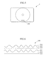
- Fig.6 shows a plane fine structure obtained by enlarging the parallel groove continuity 100 described in Figs. 3 to 5 .
- P ⁇ ⁇ /NA is established when the pitch between the track 201 having the wobbling groove region and the track 203 having the linear groove region is P, the wavelength of reproduction light for reproducing the information recording carrier 1 of the present invention is ⁇ and the numerical aperture of an objective lens is NA.
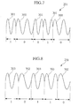
- Fig. 7 shows an example in which data 1, 0, 1, 1, 0 are recorded in a shape, comprising high frequency portions 301 and low frequency portions 300.
- Fig.9 shows an example in which the high frequency portion 301 and the low frequency portion 302 are allocated to maintain the phase continuity at the switching point of the channel bit in the wobbling groove region 221 in order to improve such a problem.
- demodulating circuit can be simplified. Further, a circuit having the 0.5 window facilitates generation of clocks. Further, demodulation can be executed by means of a synchronous detection circuit.
- the entire information recording carrier is viewed, it is comprised of three spirals for the track 201, the inter-groove portion 202 and the track 203.
- the direct recording may generate continuation of 0 or 1, so that direct current component may be generated in data.
- it is permissible to adopt a method of recording base-band modulated data Namely, 0 and 1 are converted to a different code preliminarily and continuation of 0 and 1 is made below a predetermined value.
- Fig.15 shows a sectional view taken along the line CR of Fig. 14 .
- the track 201 having the wobbling groove region, the track 203 having the linear groove region and the inter-groove region 202 are disposed substantially in parallel to each other, so that they are extended vertically in the radial direction while in parallel in the tangential direction.
- the thickness of the supporting body 13 is 0.3 to 3 mm, more preferably 0.5 to 2 mm.
- the thickness of the supporting body 13 is designed so that the total thickness of the supporting body 13, the recording layer 12, the light transmission layer 11 and the like is 1.2 mm for compatibility with a conventional optical disc.
- These alloys can contain at least one element selected from groups consisting of Cu, Ba, Co, Cr, Ni, Pt, Si, Sr, Au, Cd, Li, Mo, Mn, Zn, Fe, Pb, Na, Cs, Ga, Pd, Bi, Sn, Ti, V, Ge, Se, S, As, Tl, In, Pd, Pt, Ni by 0.01 atom% or more to less than 10 atoms% in total.
- the light transmission layer 11 has the function of introducing converged reproduction light to the recording layer 12 with little optical distortion.
- deflection in the thickness in a plane is preferred to be ⁇ 0.003 mm max, because the NA of the objective lens is large. Particularly when the NA of the objective lens is more than 0.85, it is preferred to be less than ⁇ 0.002 mm. Further, if the NA of the objective lens is 0.9, preferably, the thickness is less than ⁇ 0.001 mm.
- the information recording carrier 1 of the present invention it is permissible to employ saw tooth wave as its basic wave. That is, although not shown, the saw tooth wave can take two values by mild riseup/steep fall and steep riseup/mild fall. Because interference with the data recording method of the present invention is small, multi-value data can be recorded by combination. For example, if the frequency shift modulation is binary, four value data can be recorded by combination.
- a disc like information recording carrier 1 having the structure shown in Fig.12 was manufactured.
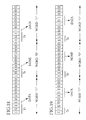
- the frequency of the low frequency portion is matched with the single frequency of the clock region 401. Further, the high frequency portion 305, the low frequency portion 304 and the clock region 401 have the same amplitude.
- address data was subjected to base band modulation with Manchester code and further differential modulation.
- the track 231 having the wobbling groove region and the track 233 having the linear groove region are disposed in the land portion L in Fig.13 while the inter-groove portion 232 is disposed in the groove portion G.
- a phase rewritable disc having the recording layer 12 made of mainly Ge doping SbTe was employed and this information recording carrier 1 which could execute recording/reproduction through the 0.1 mm light transmission layer 11 was completed.
Landscapes
- Optical Recording Or Reproduction (AREA)
- Optical Record Carriers And Manufacture Thereof (AREA)
- Signal Processing For Digital Recording And Reproducing (AREA)
Applications Claiming Priority (3)
| Application Number | Priority Date | Filing Date | Title |
|---|---|---|---|
| JP2001286516 | 2001-09-20 | ||
| JP2002082758A JP2003168222A (ja) | 2001-09-20 | 2002-03-25 | 情報記録担体及び情報記録担体の再生方法及び情報記録担体の再生装置 |
| EP02021261A EP1296314A3 (fr) | 2001-09-20 | 2002-09-19 | Support d'enregistrement d'informations |
Related Parent Applications (2)
| Application Number | Title | Priority Date | Filing Date |
|---|---|---|---|
| EP02021261.9 Division | 2002-09-19 | ||
| EP02021261A Division EP1296314A3 (fr) | 2001-09-20 | 2002-09-19 | Support d'enregistrement d'informations |
Publications (2)
| Publication Number | Publication Date |
|---|---|
| EP2117000A1 true EP2117000A1 (fr) | 2009-11-11 |
| EP2117000B1 EP2117000B1 (fr) | 2012-12-05 |
Family
ID=26622575
Family Applications (2)
| Application Number | Title | Priority Date | Filing Date |
|---|---|---|---|
| EP09009028A Expired - Lifetime EP2117000B1 (fr) | 2001-09-20 | 2002-09-19 | Support d'enregistrement d'informations |
| EP02021261A Withdrawn EP1296314A3 (fr) | 2001-09-20 | 2002-09-19 | Support d'enregistrement d'informations |
Family Applications After (1)
| Application Number | Title | Priority Date | Filing Date |
|---|---|---|---|
| EP02021261A Withdrawn EP1296314A3 (fr) | 2001-09-20 | 2002-09-19 | Support d'enregistrement d'informations |
Country Status (4)
| Country | Link |
|---|---|
| US (11) | US7088670B2 (fr) |
| EP (2) | EP2117000B1 (fr) |
| JP (1) | JP2003168222A (fr) |
| CN (2) | CN1199167C (fr) |
Families Citing this family (16)
| Publication number | Priority date | Publication date | Assignee | Title |
|---|---|---|---|---|
| DE60043406D1 (de) * | 1999-11-25 | 2010-01-07 | Victor Company Of Japan | Medium zur Aufzeichnung optischer Informationen sowie Substrat und Herstellungsverfahren für das Medium zur Aufzeichnung optischer Informationen |
| US7133331B2 (en) * | 2000-12-28 | 2006-11-07 | Victor Company Of Japan, Limited | Recording medium having a substrate containing microscopic pattern of parallel groove and land sections and recording/reproducing equipment therefor |
| TW583650B (en) | 2001-06-18 | 2004-04-11 | Samsung Electronics Co Ltd | Optical recording medium |
| JP2003168222A (ja) * | 2001-09-20 | 2003-06-13 | Victor Co Of Japan Ltd | 情報記録担体及び情報記録担体の再生方法及び情報記録担体の再生装置 |
| US7406022B2 (en) * | 2002-03-15 | 2008-07-29 | Samsung Electronics Co., Ltd. | Optical recording medium |
| US7177262B2 (en) * | 2002-04-19 | 2007-02-13 | Victor Company Of Japan, Ltd. | Reproducing system and corresponding information recording medium having wobbled land portions |
| US7425735B2 (en) * | 2003-02-24 | 2008-09-16 | Samsung Electronics Co., Ltd. | Multi-layer phase-changeable memory devices |
| US7402851B2 (en) * | 2003-02-24 | 2008-07-22 | Samsung Electronics Co., Ltd. | Phase changeable memory devices including nitrogen and/or silicon and methods for fabricating the same |
| US7115927B2 (en) * | 2003-02-24 | 2006-10-03 | Samsung Electronics Co., Ltd. | Phase changeable memory devices |
| JP2005032290A (ja) * | 2003-07-07 | 2005-02-03 | Ricoh Co Ltd | 情報記録媒体及び光ディスク装置 |
| JP2006099926A (ja) * | 2004-09-06 | 2006-04-13 | Sanyo Electric Co Ltd | 光磁気記録媒体および層構造 |
| JP4393340B2 (ja) * | 2004-10-19 | 2010-01-06 | 三洋電機株式会社 | 光記録媒体、光記録方法、光再生方法、光記録装置および光再生装置。 |
| KR100782482B1 (ko) * | 2006-05-19 | 2007-12-05 | 삼성전자주식회사 | GeBiTe막을 상변화 물질막으로 채택하는 상변화 기억 셀, 이를 구비하는 상변화 기억소자, 이를 구비하는 전자 장치 및 그 제조방법 |
| KR100810615B1 (ko) * | 2006-09-20 | 2008-03-06 | 삼성전자주식회사 | 고온 상전이 패턴을 구비한 상전이 메모리소자 및 그제조방법 |
| JP6794353B2 (ja) | 2014-11-07 | 2020-12-02 | オハイオ・ステート・イノヴェーション・ファウンデーション | アンビエント照明条件において眼についての判定を行うための方法及び装置 |
| TWI680648B (zh) * | 2018-12-26 | 2019-12-21 | 財團法人工業技術研究院 | 編碼盤、檢光器、光學絕對式旋轉編碼器及編碼值輸出、偵錯與除錯的方法 |
Citations (7)
| Publication number | Priority date | Publication date | Assignee | Title |
|---|---|---|---|---|
| JP2778405B2 (ja) | 1993-03-12 | 1998-07-23 | 日亜化学工業株式会社 | 窒化ガリウム系化合物半導体発光素子 |
| EP0930611A1 (fr) * | 1996-09-26 | 1999-07-21 | SANYO ELECTRIC Co., Ltd. | Support d'enregistrement et appareil de reproduction correspondant |
| JPH11346154A (ja) | 1998-05-29 | 1999-12-14 | Sony Corp | 変調装置および方法、復調装置および方法、並びに提供媒体 |
| JP2000286709A (ja) | 1999-01-29 | 2000-10-13 | Victor Co Of Japan Ltd | 変調方法、変調装置、復調方法、復調装置及び記録媒体 |
| JP2000332613A (ja) | 1999-05-25 | 2000-11-30 | Victor Co Of Japan Ltd | 変調装置、復調装置 |
| JP2001080205A (ja) | 1999-09-10 | 2001-03-27 | Canon Inc | インクジェット用記録媒体、これを用いたインクジェット記録方法 |
| EP1115109A2 (fr) * | 1999-12-10 | 2001-07-11 | Sony Corporation | Disque optique et appareil de disque optique |
Family Cites Families (21)
| Publication number | Priority date | Publication date | Assignee | Title |
|---|---|---|---|---|
| US599504A (en) * | 1898-02-22 | Type-writer-ribbon holder | ||
| JP3226295B2 (ja) | 1991-06-03 | 2001-11-05 | 株式会社日立製作所 | 伝送信号処理装置及び復調方法 |
| JP2653284B2 (ja) | 1991-10-09 | 1997-09-17 | 松下電器産業株式会社 | データ同期検出装置 |
| JPH05282705A (ja) | 1992-04-01 | 1993-10-29 | Matsushita Electric Ind Co Ltd | 光ディスク |
| JP3227976B2 (ja) | 1993-02-26 | 2001-11-12 | 松下電器産業株式会社 | 光学的情報記録部材、記録再生方法、及び記録再生装置 |
| JP3201235B2 (ja) | 1995-10-23 | 2001-08-20 | 株式会社日立製作所 | 情報記録媒体、記録制御情報再生方法及び情報記録再生装置 |
| JP3772379B2 (ja) | 1996-03-25 | 2006-05-10 | ソニー株式会社 | 記録媒体、アドレス記録方法、および装置 |
| JP3418065B2 (ja) * | 1996-06-26 | 2003-06-16 | 三菱電機株式会社 | 光ディスク |
| JPH1074321A (ja) | 1996-07-05 | 1998-03-17 | Sharp Corp | 光ディスク基板及びその製造方法並びに光ディスク及びその再生方法 |
| JPH1069646A (ja) | 1996-08-29 | 1998-03-10 | Ricoh Co Ltd | 光ディスク媒体、光ディスク装置 |
| JPH10208249A (ja) * | 1997-01-21 | 1998-08-07 | Sony Corp | 光ディスク |
| JPH10302310A (ja) | 1997-04-25 | 1998-11-13 | Sony Corp | 光学記録媒体及び光学ディスク装置 |
| JP4144054B2 (ja) * | 1997-07-24 | 2008-09-03 | ソニー株式会社 | 光ディスクの記録方法 |
| JPH1166618A (ja) | 1997-08-21 | 1999-03-09 | Sony Corp | 光記録媒体及びその製造方法 |
| JPH1196579A (ja) * | 1997-09-19 | 1999-04-09 | Tdk Corp | 光記録媒体の記録再生方法および光記録媒体 |
| JP2000187882A (ja) | 1998-02-24 | 2000-07-04 | Sony Corp | 光記録媒体 |
| JP2000011453A (ja) * | 1998-06-29 | 2000-01-14 | Sony Corp | 光記録媒体と光記録再生装置 |
| ZA200005575B (en) | 1999-10-25 | 2001-05-03 | Rohm & Haas | Preparation of an aqueous composition for treating leather. |
| JP2003022580A (ja) * | 2001-05-02 | 2003-01-24 | Victor Co Of Japan Ltd | 情報記録担体、情報記録担体の製造方法、情報記録担体再生装置及び情報記録担体記録装置 |
| JP2003168222A (ja) * | 2001-09-20 | 2003-06-13 | Victor Co Of Japan Ltd | 情報記録担体及び情報記録担体の再生方法及び情報記録担体の再生装置 |
| JP2003173543A (ja) * | 2001-09-26 | 2003-06-20 | Victor Co Of Japan Ltd | 情報記録担体及び情報記録担体の再生方法及び情報記録担体の再生装置 |
-
2002
- 2002-03-25 JP JP2002082758A patent/JP2003168222A/ja active Pending
- 2002-09-18 CN CNB021426996A patent/CN1199167C/zh not_active Expired - Lifetime
- 2002-09-18 CN CNB2005100527063A patent/CN1326139C/zh not_active Expired - Lifetime
- 2002-09-18 US US10/245,757 patent/US7088670B2/en not_active Expired - Lifetime
- 2002-09-19 EP EP09009028A patent/EP2117000B1/fr not_active Expired - Lifetime
- 2002-09-19 EP EP02021261A patent/EP1296314A3/fr not_active Withdrawn
-
2006
- 2006-05-16 US US11/434,136 patent/US7391709B2/en not_active Expired - Lifetime
- 2006-05-16 US US11/434,186 patent/US7505393B2/en not_active Expired - Fee Related
-
2008
- 2008-05-20 US US12/153,497 patent/US7876669B2/en not_active Expired - Fee Related
- 2008-05-20 US US12/153,498 patent/US7639594B2/en not_active Expired - Fee Related
- 2008-10-07 US US12/285,503 patent/US7643402B2/en not_active Expired - Fee Related
- 2008-10-07 US US12/285,504 patent/US7643403B2/en not_active Expired - Fee Related
-
2009
- 2009-01-16 US US12/320,081 patent/US7701837B2/en not_active Expired - Fee Related
- 2009-01-16 US US12/320,096 patent/US7636296B2/en not_active Expired - Fee Related
- 2009-11-24 US US12/591,582 patent/US7796496B2/en not_active Expired - Fee Related
- 2009-11-24 US US12/591,583 patent/US7796497B2/en not_active Expired - Fee Related
Patent Citations (7)
| Publication number | Priority date | Publication date | Assignee | Title |
|---|---|---|---|---|
| JP2778405B2 (ja) | 1993-03-12 | 1998-07-23 | 日亜化学工業株式会社 | 窒化ガリウム系化合物半導体発光素子 |
| EP0930611A1 (fr) * | 1996-09-26 | 1999-07-21 | SANYO ELECTRIC Co., Ltd. | Support d'enregistrement et appareil de reproduction correspondant |
| JPH11346154A (ja) | 1998-05-29 | 1999-12-14 | Sony Corp | 変調装置および方法、復調装置および方法、並びに提供媒体 |
| JP2000286709A (ja) | 1999-01-29 | 2000-10-13 | Victor Co Of Japan Ltd | 変調方法、変調装置、復調方法、復調装置及び記録媒体 |
| JP2000332613A (ja) | 1999-05-25 | 2000-11-30 | Victor Co Of Japan Ltd | 変調装置、復調装置 |
| JP2001080205A (ja) | 1999-09-10 | 2001-03-27 | Canon Inc | インクジェット用記録媒体、これを用いたインクジェット記録方法 |
| EP1115109A2 (fr) * | 1999-12-10 | 2001-07-11 | Sony Corporation | Disque optique et appareil de disque optique |
Also Published As
| Publication number | Publication date |
|---|---|
| CN1326139C (zh) | 2007-07-11 |
| US7796497B2 (en) | 2010-09-14 |
| US7643402B2 (en) | 2010-01-05 |
| US20090040915A1 (en) | 2009-02-12 |
| US20090135709A1 (en) | 2009-05-28 |
| US20090135710A1 (en) | 2009-05-28 |
| JP2003168222A (ja) | 2003-06-13 |
| US20060233092A1 (en) | 2006-10-19 |
| US7505393B2 (en) | 2009-03-17 |
| US20090067312A1 (en) | 2009-03-12 |
| US7876669B2 (en) | 2011-01-25 |
| US20060239175A1 (en) | 2006-10-26 |
| US20100074088A1 (en) | 2010-03-25 |
| EP1296314A2 (fr) | 2003-03-26 |
| EP2117000B1 (fr) | 2012-12-05 |
| US20030053405A1 (en) | 2003-03-20 |
| US7391709B2 (en) | 2008-06-24 |
| US20100074087A1 (en) | 2010-03-25 |
| US7636296B2 (en) | 2009-12-22 |
| US7088670B2 (en) | 2006-08-08 |
| CN1405766A (zh) | 2003-03-26 |
| EP1296314A3 (fr) | 2007-08-01 |
| US7796496B2 (en) | 2010-09-14 |
| US7639594B2 (en) | 2009-12-29 |
| US7643403B2 (en) | 2010-01-05 |
| US7701837B2 (en) | 2010-04-20 |
| US20080316908A1 (en) | 2008-12-25 |
| US20080259782A1 (en) | 2008-10-23 |
| CN1199167C (zh) | 2005-04-27 |
| CN1677524A (zh) | 2005-10-05 |
Similar Documents
| Publication | Publication Date | Title |
|---|---|---|
| US7796496B2 (en) | Information recording carrier and method of reproducing the same | |
| US7911924B2 (en) | Information recording carrier and information reproducing apparatus for the same |
Legal Events
| Date | Code | Title | Description |
|---|---|---|---|
| PUAI | Public reference made under article 153(3) epc to a published international application that has entered the european phase |
Free format text: ORIGINAL CODE: 0009012 |
|
| AC | Divisional application: reference to earlier application |
Ref document number: 1296314 Country of ref document: EP Kind code of ref document: P |
|
| AK | Designated contracting states |
Kind code of ref document: A1 Designated state(s): DE FR GB |
|
| RIN1 | Information on inventor provided before grant (corrected) |
Inventor name: THE INVENTOR HAS AGREED TO WAIVE HIS ENTITLEMENT T |
|
| 17P | Request for examination filed |
Effective date: 20100511 |
|
| 17Q | First examination report despatched |
Effective date: 20101022 |
|
| REG | Reference to a national code |
Ref country code: DE Ref legal event code: R079 Ref document number: 60244192 Country of ref document: DE Free format text: PREVIOUS MAIN CLASS: G11B0007007000 Ipc: G11B0027240000 |
|
| GRAP | Despatch of communication of intention to grant a patent |
Free format text: ORIGINAL CODE: EPIDOSNIGR1 |
|
| RIC1 | Information provided on ipc code assigned before grant |
Ipc: G11B 27/24 20060101AFI20111209BHEP Ipc: G11B 7/007 20060101ALI20111209BHEP |
|
| RAP1 | Party data changed (applicant data changed or rights of an application transferred) |
Owner name: JVC KENWOOD CORPORATION |
|
| GRAS | Grant fee paid |
Free format text: ORIGINAL CODE: EPIDOSNIGR3 |
|
| RIN1 | Information on inventor provided before grant (corrected) |
Inventor name: THE INVENTOR HAS AGREED TO WAIVE HIS ENTITLEMENT T |
|
| GRAA | (expected) grant |
Free format text: ORIGINAL CODE: 0009210 |
|
| AC | Divisional application: reference to earlier application |
Ref document number: 1296314 Country of ref document: EP Kind code of ref document: P |
|
| AK | Designated contracting states |
Kind code of ref document: B1 Designated state(s): DE FR GB |
|
| REG | Reference to a national code |
Ref country code: GB Ref legal event code: FG4D |
|
| REG | Reference to a national code |
Ref country code: DE Ref legal event code: R096 Ref document number: 60244192 Country of ref document: DE Effective date: 20130124 |
|
| PLBE | No opposition filed within time limit |
Free format text: ORIGINAL CODE: 0009261 |
|
| STAA | Information on the status of an ep patent application or granted ep patent |
Free format text: STATUS: NO OPPOSITION FILED WITHIN TIME LIMIT |
|
| 26N | No opposition filed |
Effective date: 20130906 |
|
| REG | Reference to a national code |
Ref country code: DE Ref legal event code: R097 Ref document number: 60244192 Country of ref document: DE Effective date: 20130906 |
|
| REG | Reference to a national code |
Ref country code: FR Ref legal event code: PLFP Year of fee payment: 15 |
|
| REG | Reference to a national code |
Ref country code: FR Ref legal event code: PLFP Year of fee payment: 16 |
|
| REG | Reference to a national code |
Ref country code: FR Ref legal event code: PLFP Year of fee payment: 17 |
|
| PGFP | Annual fee paid to national office [announced via postgrant information from national office to epo] |
Ref country code: FR Payment date: 20210812 Year of fee payment: 20 |
|
| PGFP | Annual fee paid to national office [announced via postgrant information from national office to epo] |
Ref country code: GB Payment date: 20210811 Year of fee payment: 20 Ref country code: DE Payment date: 20210810 Year of fee payment: 20 |
|
| REG | Reference to a national code |
Ref country code: DE Ref legal event code: R071 Ref document number: 60244192 Country of ref document: DE |
|
| REG | Reference to a national code |
Ref country code: GB Ref legal event code: PE20 Expiry date: 20220918 |
|
| PG25 | Lapsed in a contracting state [announced via postgrant information from national office to epo] |
Ref country code: GB Free format text: LAPSE BECAUSE OF EXPIRATION OF PROTECTION Effective date: 20220918 |