EP2117008A1 - Pâte résistive et condensateur céramique empilé - Google Patents
Pâte résistive et condensateur céramique empilé Download PDFInfo
- Publication number
- EP2117008A1 EP2117008A1 EP08704236A EP08704236A EP2117008A1 EP 2117008 A1 EP2117008 A1 EP 2117008A1 EP 08704236 A EP08704236 A EP 08704236A EP 08704236 A EP08704236 A EP 08704236A EP 2117008 A1 EP2117008 A1 EP 2117008A1
- Authority
- EP
- European Patent Office
- Prior art keywords
- densification
- resistive
- pass
- electrode layer
- resistive paste
- Prior art date
- Legal status (The legal status is an assumption and is not a legal conclusion. Google has not performed a legal analysis and makes no representation as to the accuracy of the status listed.)
- Granted
Links
Images



Classifications
-
- H—ELECTRICITY
- H01—ELECTRIC ELEMENTS
- H01B—CABLES; CONDUCTORS; INSULATORS; SELECTION OF MATERIALS FOR THEIR CONDUCTIVE, INSULATING OR DIELECTRIC PROPERTIES
- H01B1/00—Conductors or conductive bodies characterised by the conductive materials; Selection of materials as conductors
- H01B1/20—Conductive material dispersed in non-conductive organic material
-
- H—ELECTRICITY
- H01—ELECTRIC ELEMENTS
- H01G—CAPACITORS; CAPACITORS, RECTIFIERS, DETECTORS, SWITCHING DEVICES, LIGHT-SENSITIVE OR TEMPERATURE-SENSITIVE DEVICES OF THE ELECTROLYTIC TYPE
- H01G4/00—Fixed capacitors; Processes of their manufacture
- H01G4/002—Details
- H01G4/228—Terminals
- H01G4/232—Terminals electrically connecting two or more layers of a stacked or rolled capacitor
- H01G4/2325—Terminals electrically connecting two or more layers of a stacked or rolled capacitor characterised by the material of the terminals
-
- C—CHEMISTRY; METALLURGY
- C04—CEMENTS; CONCRETE; ARTIFICIAL STONE; CERAMICS; REFRACTORIES
- C04B—LIME, MAGNESIA; SLAG; CEMENTS; COMPOSITIONS THEREOF, e.g. MORTARS, CONCRETE OR LIKE BUILDING MATERIALS; ARTIFICIAL STONE; CERAMICS; REFRACTORIES; TREATMENT OF NATURAL STONE
- C04B35/00—Shaped ceramic products characterised by their composition; Ceramics compositions; Processing powders of inorganic compounds preparatory to the manufacturing of ceramic products
- C04B35/01—Shaped ceramic products characterised by their composition; Ceramics compositions; Processing powders of inorganic compounds preparatory to the manufacturing of ceramic products based on oxide ceramics
- C04B35/453—Shaped ceramic products characterised by their composition; Ceramics compositions; Processing powders of inorganic compounds preparatory to the manufacturing of ceramic products based on oxide ceramics based on zinc, tin, or bismuth oxides or solid solutions thereof with other oxides, e.g. zincates, stannates or bismuthates
- C04B35/457—Shaped ceramic products characterised by their composition; Ceramics compositions; Processing powders of inorganic compounds preparatory to the manufacturing of ceramic products based on oxide ceramics based on zinc, tin, or bismuth oxides or solid solutions thereof with other oxides, e.g. zincates, stannates or bismuthates based on tin oxides or stannates
-
- C—CHEMISTRY; METALLURGY
- C22—METALLURGY; FERROUS OR NON-FERROUS ALLOYS; TREATMENT OF ALLOYS OR NON-FERROUS METALS
- C22C—ALLOYS
- C22C29/00—Alloys based on carbides, oxides, nitrides, borides, or silicides, e.g. cermets, or other metal compounds, e.g. oxynitrides, sulfides
- C22C29/12—Alloys based on carbides, oxides, nitrides, borides, or silicides, e.g. cermets, or other metal compounds, e.g. oxynitrides, sulfides based on oxides
-
- H—ELECTRICITY
- H01—ELECTRIC ELEMENTS
- H01B—CABLES; CONDUCTORS; INSULATORS; SELECTION OF MATERIALS FOR THEIR CONDUCTIVE, INSULATING OR DIELECTRIC PROPERTIES
- H01B1/00—Conductors or conductive bodies characterised by the conductive materials; Selection of materials as conductors
- H01B1/20—Conductive material dispersed in non-conductive organic material
- H01B1/22—Conductive material dispersed in non-conductive organic material the conductive material comprising metals or alloys
-
- H—ELECTRICITY
- H01—ELECTRIC ELEMENTS
- H01G—CAPACITORS; CAPACITORS, RECTIFIERS, DETECTORS, SWITCHING DEVICES, LIGHT-SENSITIVE OR TEMPERATURE-SENSITIVE DEVICES OF THE ELECTROLYTIC TYPE
- H01G4/00—Fixed capacitors; Processes of their manufacture
- H01G4/002—Details
- H01G4/018—Dielectrics
- H01G4/06—Solid dielectrics
- H01G4/08—Inorganic dielectrics
- H01G4/12—Ceramic dielectrics
-
- H—ELECTRICITY
- H01—ELECTRIC ELEMENTS
- H01G—CAPACITORS; CAPACITORS, RECTIFIERS, DETECTORS, SWITCHING DEVICES, LIGHT-SENSITIVE OR TEMPERATURE-SENSITIVE DEVICES OF THE ELECTROLYTIC TYPE
- H01G4/00—Fixed capacitors; Processes of their manufacture
- H01G4/30—Stacked capacitors
-
- C—CHEMISTRY; METALLURGY
- C04—CEMENTS; CONCRETE; ARTIFICIAL STONE; CERAMICS; REFRACTORIES
- C04B—LIME, MAGNESIA; SLAG; CEMENTS; COMPOSITIONS THEREOF, e.g. MORTARS, CONCRETE OR LIKE BUILDING MATERIALS; ARTIFICIAL STONE; CERAMICS; REFRACTORIES; TREATMENT OF NATURAL STONE
- C04B2235/00—Aspects relating to ceramic starting mixtures or sintered ceramic products
- C04B2235/02—Composition of constituents of the starting material or of secondary phases of the final product
- C04B2235/30—Constituents and secondary phases not being of a fibrous nature
- C04B2235/32—Metal oxides, mixed metal oxides, or oxide-forming salts thereof, e.g. carbonates, nitrates, (oxy)hydroxides, chlorides
- C04B2235/3217—Aluminum oxide or oxide forming salts thereof, e.g. bauxite, alpha-alumina
-
- C—CHEMISTRY; METALLURGY
- C04—CEMENTS; CONCRETE; ARTIFICIAL STONE; CERAMICS; REFRACTORIES
- C04B—LIME, MAGNESIA; SLAG; CEMENTS; COMPOSITIONS THEREOF, e.g. MORTARS, CONCRETE OR LIKE BUILDING MATERIALS; ARTIFICIAL STONE; CERAMICS; REFRACTORIES; TREATMENT OF NATURAL STONE
- C04B2235/00—Aspects relating to ceramic starting mixtures or sintered ceramic products
- C04B2235/02—Composition of constituents of the starting material or of secondary phases of the final product
- C04B2235/30—Constituents and secondary phases not being of a fibrous nature
- C04B2235/32—Metal oxides, mixed metal oxides, or oxide-forming salts thereof, e.g. carbonates, nitrates, (oxy)hydroxides, chlorides
- C04B2235/3231—Refractory metal oxides, their mixed metal oxides, or oxide-forming salts thereof
- C04B2235/3232—Titanium oxides or titanates, e.g. rutile or anatase
-
- C—CHEMISTRY; METALLURGY
- C04—CEMENTS; CONCRETE; ARTIFICIAL STONE; CERAMICS; REFRACTORIES
- C04B—LIME, MAGNESIA; SLAG; CEMENTS; COMPOSITIONS THEREOF, e.g. MORTARS, CONCRETE OR LIKE BUILDING MATERIALS; ARTIFICIAL STONE; CERAMICS; REFRACTORIES; TREATMENT OF NATURAL STONE
- C04B2235/00—Aspects relating to ceramic starting mixtures or sintered ceramic products
- C04B2235/02—Composition of constituents of the starting material or of secondary phases of the final product
- C04B2235/30—Constituents and secondary phases not being of a fibrous nature
- C04B2235/32—Metal oxides, mixed metal oxides, or oxide-forming salts thereof, e.g. carbonates, nitrates, (oxy)hydroxides, chlorides
- C04B2235/3231—Refractory metal oxides, their mixed metal oxides, or oxide-forming salts thereof
- C04B2235/3244—Zirconium oxides, zirconates, hafnium oxides, hafnates, or oxide-forming salts thereof
-
- C—CHEMISTRY; METALLURGY
- C04—CEMENTS; CONCRETE; ARTIFICIAL STONE; CERAMICS; REFRACTORIES
- C04B—LIME, MAGNESIA; SLAG; CEMENTS; COMPOSITIONS THEREOF, e.g. MORTARS, CONCRETE OR LIKE BUILDING MATERIALS; ARTIFICIAL STONE; CERAMICS; REFRACTORIES; TREATMENT OF NATURAL STONE
- C04B2235/00—Aspects relating to ceramic starting mixtures or sintered ceramic products
- C04B2235/02—Composition of constituents of the starting material or of secondary phases of the final product
- C04B2235/30—Constituents and secondary phases not being of a fibrous nature
- C04B2235/32—Metal oxides, mixed metal oxides, or oxide-forming salts thereof, e.g. carbonates, nitrates, (oxy)hydroxides, chlorides
- C04B2235/3284—Zinc oxides, zincates, cadmium oxides, cadmiates, mercury oxides, mercurates or oxide forming salts thereof
-
- C—CHEMISTRY; METALLURGY
- C04—CEMENTS; CONCRETE; ARTIFICIAL STONE; CERAMICS; REFRACTORIES
- C04B—LIME, MAGNESIA; SLAG; CEMENTS; COMPOSITIONS THEREOF, e.g. MORTARS, CONCRETE OR LIKE BUILDING MATERIALS; ARTIFICIAL STONE; CERAMICS; REFRACTORIES; TREATMENT OF NATURAL STONE
- C04B2235/00—Aspects relating to ceramic starting mixtures or sintered ceramic products
- C04B2235/02—Composition of constituents of the starting material or of secondary phases of the final product
- C04B2235/30—Constituents and secondary phases not being of a fibrous nature
- C04B2235/32—Metal oxides, mixed metal oxides, or oxide-forming salts thereof, e.g. carbonates, nitrates, (oxy)hydroxides, chlorides
- C04B2235/3286—Gallium oxides, gallates, indium oxides, indates, thallium oxides, thallates or oxide forming salts thereof, e.g. zinc gallate
-
- C—CHEMISTRY; METALLURGY
- C04—CEMENTS; CONCRETE; ARTIFICIAL STONE; CERAMICS; REFRACTORIES
- C04B—LIME, MAGNESIA; SLAG; CEMENTS; COMPOSITIONS THEREOF, e.g. MORTARS, CONCRETE OR LIKE BUILDING MATERIALS; ARTIFICIAL STONE; CERAMICS; REFRACTORIES; TREATMENT OF NATURAL STONE
- C04B2235/00—Aspects relating to ceramic starting mixtures or sintered ceramic products
- C04B2235/02—Composition of constituents of the starting material or of secondary phases of the final product
- C04B2235/30—Constituents and secondary phases not being of a fibrous nature
- C04B2235/36—Glass starting materials for making ceramics, e.g. silica glass
-
- C—CHEMISTRY; METALLURGY
- C04—CEMENTS; CONCRETE; ARTIFICIAL STONE; CERAMICS; REFRACTORIES
- C04B—LIME, MAGNESIA; SLAG; CEMENTS; COMPOSITIONS THEREOF, e.g. MORTARS, CONCRETE OR LIKE BUILDING MATERIALS; ARTIFICIAL STONE; CERAMICS; REFRACTORIES; TREATMENT OF NATURAL STONE
- C04B2235/00—Aspects relating to ceramic starting mixtures or sintered ceramic products
- C04B2235/02—Composition of constituents of the starting material or of secondary phases of the final product
- C04B2235/30—Constituents and secondary phases not being of a fibrous nature
- C04B2235/40—Metallic constituents or additives not added as binding phase
- C04B2235/404—Refractory metals
-
- C—CHEMISTRY; METALLURGY
- C04—CEMENTS; CONCRETE; ARTIFICIAL STONE; CERAMICS; REFRACTORIES
- C04B—LIME, MAGNESIA; SLAG; CEMENTS; COMPOSITIONS THEREOF, e.g. MORTARS, CONCRETE OR LIKE BUILDING MATERIALS; ARTIFICIAL STONE; CERAMICS; REFRACTORIES; TREATMENT OF NATURAL STONE
- C04B2235/00—Aspects relating to ceramic starting mixtures or sintered ceramic products
- C04B2235/02—Composition of constituents of the starting material or of secondary phases of the final product
- C04B2235/30—Constituents and secondary phases not being of a fibrous nature
- C04B2235/40—Metallic constituents or additives not added as binding phase
- C04B2235/405—Iron group metals
-
- C—CHEMISTRY; METALLURGY
- C04—CEMENTS; CONCRETE; ARTIFICIAL STONE; CERAMICS; REFRACTORIES
- C04B—LIME, MAGNESIA; SLAG; CEMENTS; COMPOSITIONS THEREOF, e.g. MORTARS, CONCRETE OR LIKE BUILDING MATERIALS; ARTIFICIAL STONE; CERAMICS; REFRACTORIES; TREATMENT OF NATURAL STONE
- C04B2235/00—Aspects relating to ceramic starting mixtures or sintered ceramic products
- C04B2235/02—Composition of constituents of the starting material or of secondary phases of the final product
- C04B2235/30—Constituents and secondary phases not being of a fibrous nature
- C04B2235/40—Metallic constituents or additives not added as binding phase
- C04B2235/407—Copper
-
- C—CHEMISTRY; METALLURGY
- C04—CEMENTS; CONCRETE; ARTIFICIAL STONE; CERAMICS; REFRACTORIES
- C04B—LIME, MAGNESIA; SLAG; CEMENTS; COMPOSITIONS THEREOF, e.g. MORTARS, CONCRETE OR LIKE BUILDING MATERIALS; ARTIFICIAL STONE; CERAMICS; REFRACTORIES; TREATMENT OF NATURAL STONE
- C04B2235/00—Aspects relating to ceramic starting mixtures or sintered ceramic products
- C04B2235/70—Aspects relating to sintered or melt-casted ceramic products
- C04B2235/74—Physical characteristics
- C04B2235/77—Density
Definitions
- the present invention relates to a resistive paste and a monolithic ceramic capacitor manufactured using the resistive paste and, more particularly, to a resistive paste that is advantageously used to form at least part of an external electrode in order to impart the function of a CR composite electronic component to a monolithic ceramic capacitor and a monolithic ceramic capacitor manufactured using the resistive paste.
- one proposed monolithic ceramic capacitor includes an external electrode that also functions as a resistance element.
- Patent Document 1 International Publication WO 2006/022258 (Patent Document 1) describes a monolithic ceramic capacitor that includes an internal electrode containing Ni or a Ni alloy, in which an external electrode has sufficient reduction resistance and includes a resistive electrode layer, which includes an In-Sn complex oxide (ITO) reactive to the Ni or Ni alloy contained in the internal electrode and a glass component.
- ITO In-Sn complex oxide
- the external electrode can have sufficient resistance, a conductive layer for continuity between the external electrode and the internal electrode is not needed under the resistive electrode layer, and a protective layer for protecting the resistive electrode layer does not require an expensive inoxidizable metal.
- Patent Document 1 also discloses that part of ITO is substituted by Ag, Al 2 O 3 , or ZrO 2 to control the resistance.
- the substitution rate of Ag, Al 2 O 3 , or ZrO 2 for example, to increase the resistance may lead to the occurrence of blisters due to over-sintering or reduced denseness due to insufficient sintering.
- the resistive electrode layer has a constant resistance, the ESR may easily vary with the dimensions of a ceramic laminate, which is a component of the monolithic ceramic capacitor, the thickness of the resistive electrode layer, and the number of laminated layers in the internal electrode.
- resistive pastes having different substitution rates of Ag, Al 2 O 3 , or ZrO 2 for different designs must be prepared to achieve a desired ESR.
- the present inventors found that some metal species or oxide species to be substituted for part of ITO promote densification of a resistive electrode layer, and others prevent the densification, and that the metal species and/or oxide species to be substituted for part of ITO and their substitution rates can be properly determined to form a dense resistive electrode layer without causing blisters.
- the present inventors also found that, although a metal-substituted resistive paste is a low-resistance paste and an oxide-substituted resistive paste is a high-resistance paste, the low-resistance paste and the high-resistance paste can be mixed to facilitate the control of the ESR and to provide a resistive electrode layer of excellent film quality.
- the present invention is directed to a resistive paste that contains an In-Sn complex oxide, a glass frit, and an organic vehicle.
- a resistive paste according to a first aspect of the present invention further includes a densification promoting metal that promotes densification of a sintered compact formed by firing the resistive paste and is at least one selected from the group consisting of Ni and Cu; and a densification preventing metal that prevents the densification and is at least one selected from the group consisting of Mo, Cr, and Nb.
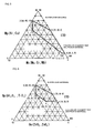
- a resistive paste according to a second aspect of the present invention further includes a densification promoting metal (Mp) that promotes densification of a sintered compact formed by firing the resistive paste and is at least one selected from the group consisting of Ni and Cu; and a densification preventing metal (Mc) that prevents the densification and is at least one selected from the group consisting of Mo, Cr, and Nb, wherein the component ratio (ITO, Mp, Mc) of the In-Sn complex oxide (ITO), the densification promoting metal (Mp), and the densification preventing metal (Mc) on the basis of volume percent is in a range included by a polygon defined by point A (95, 5, 0), point B (92.5, 5, 2.5), point C (55, 30, 15), point D (50, 40, 10), and point E (70, 30, 0) (including segments AB, BC, CD, DE, and EA) in the attached Fig. 5 .
- Mp densification promoting metal
- Mc
- a resistive paste according to a third aspect of the present invention further includes a densification promoting oxide that promotes densification of a sintered compact formed by firing the resistive paste and is at least one selected from the group consisting of Al 2 O 3 and TiO 2 ; and a densification preventing oxide that prevents the densification and is at least one selected from the group consisting of ZrO 2 and ZnO 2 .
- a resistive paste according to a fourth aspect of the present invention further includes a densification promoting oxide (Op) that promotes densification of a sintered compact formed by firing the resistive paste and is at least one selected from the group consisting of Al 2 O 3 and TiO 2 ; and densification preventing oxide (Oc) that prevents the densification and is at least one selected from the group consisting of ZrO 2 and ZnO 2 , wherein the component ratio (ITO, Op, Oc) of the In-Sn complex oxide (ITO), the densification promoting oxide (Op), and the densification preventing oxide (Oc) on the basis of volume percent is in a range included by a polygon defined by point F (78, 22, 0), point G (68, 22, 10), point H (55, 30, 15), point K (50, 40, 10), and point L (70, 30, 0) (including segments FG, GH, HK, KL, and LF) in the attached Fig. 6 .
- Op
- the resistive paste according to the first or second aspect and the resistive paste according to the third or fourth aspect may be mixed.
- the present invention is also directed to a monolithic ceramic capacitor that includes a ceramic laminate formed of a plurality of ceramic layers, internal electrodes disposed in the ceramic laminate, and an external electrode disposed on an outer surface of the ceramic laminate and electrically connected to particular internal electrodes of the internal electrodes.
- the external electrode includes a resistive electrode layer and an electroconductive electrode layer disposed on the resistive electrode layer, and the resistive electrode layer is a sintered compact of the resistive paste described above.
- a densification promoting metal or oxide that promotes densification of a sintered compact formed by firing the resistive paste can provide sufficient sintering of the sintered compact, thus improving characteristics such as moisture resistance, and a densification preventing metal or oxide that prevents the densification of the sintered compact can reduce over-sintering, thus preventing the occurrence of blisters.
- the densification promoting metals Ni and Cu and the densification preventing metals Mo, Cr, and Nb reduce the resistance of the resistive paste, whereas the densification promoting oxide Al 2 O 3 and TiO 2 and the densification preventing oxide ZrO 2 and ZnO 2 increase the resistance of the resistive paste.
- a resistive paste containing a densification promoting or preventing metal and a resistive paste containing a densification promoting or preventing oxide can be mixed to facilitate the control of the specific resistance of a sintered compact formed by firing the mixed resistive paste.
- the ESR of a monolithic ceramic capacitor that includes an external electrode including a resistive electrode layer formed of a sintered compact of a resistive paste according to the present invention can be easily controlled.
- Fig. 1 illustrates a monolithic ceramic capacitor manufactured using a resistive paste according to a first embodiment of the present invention.
- a monolithic ceramic capacitor 1 illustrated in Fig. 1 includes a ceramic laminate 3 in the shape of a rectangular parallelepiped, which includes a plurality of ceramic layers 2 each formed of dielectric ceramic.
- the ceramic laminate 3 includes internal electrodes 4 and 5 between the ceramic layers 2.
- the internal electrodes 4 and 5 contain Ni or a Ni alloy as an electroconductive component.
- the internal electrodes 4 and the internal electrodes 5 are alternately disposed with a ceramic layer 2 interposed therebetween and thereby form capacitors.
- External electrodes 6 and 7 are oppositely disposed on the outer surface of the ceramic laminate 3.
- the external electrode 6 is electrically connected to the internal electrodes 4, and the external electrode 7 is electrically connected to the internal electrodes 5.
- each of the external electrodes 6 and 7 includes a resistive electrode layer 8, which is in contact with the ceramic laminate 3 and the internal electrodes 4 or 5, and a plated electrode layer 9 disposed on the resistive electrode layer 8 and serving as an electroconductive electrode layer.
- the resistive electrode layer 8 also imparts the function of a resistance element to the external electrodes 6 and 7 and is formed of a sintered compact formed by firing a resistive paste according to the present invention, for example, in a neutral or reducing atmosphere at a temperature of approximately 700°C.
- a resistive paste according to the present invention will be described in detail below.
- the plated electrode layer 9 is formed, for example, by electroplating and preferably includes a Ni plated layer and a Sn or solder plated layer disposed on the Ni plated layer.
- the plated electrode layer 9 can improve the weatherability of the monolithic ceramic capacitor 1 and impart excellent solderability to the external electrodes 6 and 7 in the installation of the monolithic ceramic capacitor 1.
- Fig. 2 illustrates a monolithic ceramic capacitor manufactured using a resistive paste according to a second embodiment of the present invention.
- a monolithic ceramic capacitor 11 illustrated in Fig. 2 includes many of the components of the monolithic ceramic capacitor 1 illustrated in Fig. 1 . These components are denoted by the reference numerals used in Fig. 1 and will not be further described.
- each of the external electrodes 6 and 7 further includes a baked electrode layer 12 as an electroconductive electrode layer.
- the baked electrode layer 12 is disposed in contact with the outer surface of the resistive electrode layer 8 between the resistive electrode layer 8 and the plated electrode layer 9.
- the baked electrode layer 12 can be formed by applying a paste that contains a metal powder, such as a Cu powder or a Cu alloy powder, a glass frit, and an organic vehicle to the resistive electrode layer 8 and baking the paste.
- the composition of a glass component in the baked electrode layer 12 is the same as the composition of a glass component in the resistive electrode layer 8. This can stabilize the resistance of the monolithic ceramic capacitor 11 and improve the controllability of the ESR of the monolithic ceramic capacitor 11.
- the baked electrode layer 12 can further improve the weatherability of the monolithic ceramic capacitor 11 and impart sufficient plating resistance to the monolithic ceramic capacitor 11 in a plating process for forming the plated electrode layer 9.
- the resistive electrode layer 8 is formed of a sintered compact of a resistive paste according to the present invention, as described above.
- a resistive paste according to the present invention basically contains an In-Sn complex oxide, a glass frit, and an organic vehicle.
- the In-Sn complex oxide is an electroconductive component having a predetermined resistance.
- the In-Sn complex oxide is synthesized by dissolving approximately 1% to 20% by weight of SnO 2 in In 2 O 3 .
- the In-Sn complex oxide has reduced electrical conductivity.
- heat treatment required to dissolve SnO 2 must be performed at high temperature for a long period of time, thus promoting grain growth. Consequently, it takes a long period of time to pulverize grains into a powder.
- the volume ratio of the In-Sn complex oxide powder to the glass frit in the resistive paste ranges from 30:70 to 70:30.
- An excessively low content of the glass frit results in poor adhesion between In-Sn complex oxide particles, leading to a loss of the resistive electrode layer 8.
- An excessively high content of the glass frit results in a glass flow in a firing process, leading to a deformation of the resistive electrode layer 8. Because the glass component functions as an electrical insulating component, the content of the glass frit can be altered within the range described above to control the resistance of the resistive electrode layer 8 and consequently to control the ESR of the monolithic ceramic capacitor 1.
- a resistive paste in the first embodiment further contains a densification promoting metal and a densification preventing metal in place of part of the In-Sn complex oxide.
- a resistive paste in the second embodiment further contains a densification promoting oxide and a densification preventing oxide in place of part of the In-Sn complex oxide.
- the densification promoting metal or oxide promotes densification of a sintered compact formed by firing the resistive paste.
- the densification promoting metal is at least one selected from the group consisting of Ni and Cu.
- the densification promoting oxide is at least one selected from the group consisting of Al 2 O 3 and TiO 2 .
- the densification preventing metal or oxide prevents densification of a sintered compact formed by firing the resistive paste.
- the densification preventing metal is at least one selected from the group consisting of Mo, Cr, and Nb.
- the densification preventing oxide is at least one selected from the group consisting of ZrO 2 and ZnO 2 .
- the contents of the densification promoting metal and the densification preventing metal in the resistive paste according to the first embodiment are determined as described below.
- the densification promoting metal and the densification preventing metal are contained such that the component ratio (ITO, Mp, Mc) of the In-Sn complex oxide (ITO), the densification promoting metal (Mp), and the densification preventing metal (Mc) on the basis of volume percent is in a range included by a polygon defined by point A (95, 5, 0), point B (92.5, 5, 2.5), point C (55, 30, 15), point D (50, 40, 10), and point E (70, 30, 0) (including segments AB, BC, CD, DE, and EA) in the attached Fig. 5 .
- the component ratio on the segment EA in Fig. 5 it should be noted that the densification preventing metal may be absent for a particular content of the densification promoting metal.
- the contents of the densification promoting oxide and the densification preventing oxide in the resistive paste according to the second embodiment are determined as described below.
- the densification promoting oxide and the densification preventing oxide are contained such that the component ratio (ITO, Op, Oc) of the In-Sn complex oxide (ITO), the densification promoting oxide (Op), and the densification preventing oxide (Oc) on the basis of volume percent is in a range included by a polygon defined by point F (78, 22, 0), point G (68, 22, 10), point H (55, 30, 15), point K (50, 40, 10), and point L (70, 30, 0) (including segments FG, GH, HK, KL, and LF) in the attached Fig. 6 .
- the component ratio on the segment LF in Fig. 6 it should be noted that the densification preventing oxide may be absent for a particular content of the densification promoting oxide.
- the densification promoting metal or oxide can provide sufficient sintering of a sintered compact, thus improving characteristics such as moisture resistance, and the densification preventing metal or oxide can reduce over-sintering caused by the densification promoting metal or oxide, thus preventing the occurrence of blisters.
- the densification promoting metal and the densification preventing metal reduce the resistance of a resistive paste, whereas the densification promoting oxide and the densification preventing oxide increase the resistance of the resistive paste.
- the resistive paste according to the first embodiment that contains the densification promoting or preventing metal and the resistive paste according to the second embodiment that contains the densification promoting or preventing oxide can be mixed to facilitate the control of the specific resistance of a sintered compact formed by firing the mixed resistive paste.
- the ESR of the monolithic ceramic capacitors 1 and 11 can be easily controlled.
- the conductive layer is mainly composed of a metal that is reactive to a metal contained in the internal electrodes 4 and 5.
- the main component metal of the conductive layer is preferably Ni and/or Cu.
- Figs. 1 and 2 are schematic cross-sectional views of the monolithic ceramic capacitor 1 and 11 in the lamination direction, whether the external electrodes 6 and 7 are formed on the short sides or the long sides of the ceramic laminate 3 as viewed from the top is not clear. Nevertheless, the present invention can be applied to a monolithic ceramic capacitor including the external electrodes 6 and 7 formed on the short sides or the long sides of the ceramic laminate 3.
- Figs. 3 and 4 illustrate a via-array monolithic ceramic capacitor 21 as a third embodiment of a monolithic ceramic capacitor manufactured using a resistive paste according to the present invention.
- Fig. 3(a) is a top view of a monolithic ceramic capacitor 21
- Fig. 3(b) is a cross-sectional view along the line B-B in Fig. 3(a).
- Fig. 4 is an enlarged view of a portion of the via-array monolithic ceramic capacitor 21 illustrated in Fig. 3(b) .
- the monolithic ceramic capacitor 21 includes a ceramic laminate 23 in the shape of a rectangular parallelepiped, more specifically a regular quadrangular prism, which includes a plurality of ceramic layers 22 each formed of dielectric ceramic.
- the ceramic laminate 23 includes first and second via conductors 24 and 25, which pass through the ceramic laminate 23 in the lamination direction, and first and second internal electrodes 26 and 27 between the ceramic layers 22.
- the first internal electrodes 26 and the second internal electrodes 27 are alternately disposed with a ceramic layer 22 interposed therebetween and thereby form capacitors.
- the first via conductors 24 are electrically connected to the first internal electrodes 26 but are electrically insulated from the second internal electrodes 27.
- the second via conductors 25 are electrically connected to the second internal electrodes 27 but are electrically insulated from the first internal electrodes 26.
- the via conductors 24 and 25 and the internal electrodes 26 and 27 contain Ni or a Ni alloy as an electroconductive component.
- the ceramic laminate 23 further includes a plurality of first and second external electrodes 28 and 29 on the top and bottom surfaces thereof.
- the first external electrodes 28 are electrically connected to the first via conductors 24, and the second external electrodes 29 are electrically connected to the second via conductors 25. Consequently, the first external electrodes 28 are electrically connected to the first internal electrodes 26, and the second external electrodes 29 are electrically connected to the second internal electrodes 27. As illustrated in Figs. 3(a) and 3(b) , the first and second external electrodes 28 and 29 are adjacent to each other on the top and bottom surfaces of the ceramic laminate 23.
- each of the first and second external electrodes 28 and 29 includes a resistive electrode layer 30 in contact with a ceramic laminate 23 and a via conductor 24 or 25, and an electroconductive electrode layer 31 formed on the resistive electrode layer 30.
- the resistive electrode layer 30 is formed of a sintered compact formed by firing a resistive paste according to the present invention.
- the electroconductive electrode layer 31 may be formed of a plated electrode layer, a baked electrode layer, or a baked electrode layer and a plated electrode layer formed on the baked electrode layer.
- Such a via-array monolithic ceramic capacitor 21 can be manufactured as described below.
- a ceramic green sheet to be formed into the ceramic layers 22 and an electroconductive paste used to form the via conductors 24 and 25 and the internal electrodes 26 and 27 are prepared.
- the electroconductive paste is then printed on the ceramic green sheet, for example, by screen printing to form an electroconductive paste film, which is to become the internal electrodes 26 and 27.
- a predetermined number of ceramic green sheets on which the electroconductive paste film was printed are then stacked. On one side of the laminate of ceramic green sheets, a predetermined number of ceramic green sheets on which the electroconductive paste film is not printed are stacked as an outer layer. If necessary, on the other side of the laminate, ceramic green sheets are stacked as an outer layer. Through these steps, a green mother laminate has been formed. If necessary, the green mother laminate is pressed in the lamination direction, for example, by isostatic pressing.
- Through-holes passing through the mother laminate in the lamination direction are then formed, for example, with a laser or NC punch.
- the through-holes are filled with an electroconductive paste, which is to become the via conductors 24 and 25, by a method such as screen printing.
- the green mother laminate thus formed is then cut into a green ceramic laminate 23 having a predetermined size.
- the green ceramic laminate 23 is then fired.
- a resistive paste according to the present invention is printed on the top and bottom surfaces of the ceramic laminate 23 by a method such as screen printing to cover the via conductors 24 and 25 and is then baked to form the resistive electrode layers 30, which serve as bases of the first and second external electrodes 28 and 29.
- the electroconductive electrode layers 31 are formed of baked electrodes
- an electroconductive paste is printed on the resistive electrode layers 30 by a method such as screen printing and is baked to form the electroconductive electrode layers 31. If necessary, a plated electrode layer may be subsequently formed.
- the resistive electrode layers 30 are plated to form the electroconductive electrode layers 31.
- a ceramic laminate that included internal electrodes containing Ni and was used for a monolithic ceramic capacitor having a design capacitance of 1 ⁇ F was prepared by a known method.
- the ceramic laminate included 115 ceramic layers and had a width of 1600 ⁇ m and a thickness of 450 ⁇ m.
- Each of the internal electrodes had a width of 1300 ⁇ m and a thickness of 1 ⁇ m.
- External electrodes of a monolithic ceramic capacitor according to these Experimental Examples were formed on the long sides (the length of which corresponded to the width) of the ceramic laminate in a coating process described below.
- a paste used to form a resistive electrode layer was prepared as described below.
- a SnO 2 powder was mixed with an In 2 O 3 powder such that the amount of the SnO 2 powder was 5% by weight of the total amount of the In 2 O 3 powder and the SnO 2 powder.
- the mixture was calcined in the atmosphere at a temperature of 1400°C for 5 hours to sufficiently dissolve SnO 2 and was ground to prepare an In-Sn complex oxide (ITO) powder having an average particle size of approximately 1 ⁇ m.
- ITO In-Sn complex oxide
- An organic vehicle containing 20% by weight of acrylic resin was then mixed with the ITO powder and the glass frit thus prepared and was dispersed with a rolling mill to prepare a paste used for a resistive electrode layer.
- the volume ratio of (ITO powder):(glass frit):(organic vehicle) in the paste was 12.5:12.5:75.
- the volume ratio of (ITO powder):(glass frit) was 50:50, and the weight ratio of (ITO powder) : (glass frit) was 70:30.
- the paste used for a resistive electrode layer described above had a basic composition without a densification promoting metal or oxide or a densification preventing metal or oxide.
- part of the ITO powder was substituted by a densification promoting metal or oxide powder or a densification preventing metal or oxide powder each having an average particle size of approximately 1 ⁇ m.
- the paste used for a resistive electrode layer was then applied to ends of the ceramic laminate by a dip method and was dried at a temperature of 150°C for 10 minutes.
- the dry film thickness was approximately 30 ⁇ m.
- the ceramic laminate on which the paste used for a resistive electrode layer was dried was heat-treated in a N 2 atmosphere (oxygen content: 10 ppm or less) at a maximum temperature of 700°C for 15 minutes in a continuous belt furnace to form a resistive electrode layer.
- a known Cu paste that contains a Cu powder, a glass frit, and an organic vehicle was used to form a baked electrode layer on the resistive electrode layer by baking.
- the baked electrode layer was then plated with Ni and Sn to form a plated electrode layer, completing a monolithic ceramic capacitor.
- the glass frit in the paste used for a baked electrode layer was the same as the glass frit in the paste used for a resistive electrode layer.
- the ESR of the monolithic ceramic capacitor thus manufactured was measured.
- the incidence of blister was determined by polishing the cross section of the monolithic ceramic capacitor and inspecting the cross section for pores having a minor axis of 10 ⁇ m or more, which indicated the occurrence of blisters, in the resistive electrode layer.
- the relative density of the resistive electrode layer in the monolithic ceramic capacitor was determined.
- the monolithic ceramic capacitor was subjected to a humidity test at a temperature of 85°C, a relative humidity of 90%, and an applied voltage of 5 V. The elapsed time during which the insulation resistance decreased from the initial insulation resistance by one order of magnitude was considered as the life.
- the ESR, the relative density of the resistive electrode layer, and the life in a humidity test were mean values of several tens of monolithic ceramic capacitors.
- the incidence of blister was determined as the percentage of monolithic ceramic capacitors having blisters in several tens of monolithic ceramic capacitors.
- Table 1 shows that the substitution of Ni, Cu, Mo, Nb, or Cr for part of ITO can reduce the ESR with an increase in substitution rate.
- the relative density of the resistive electrode layer shows that Ni and Cu promote the densification of the resistive electrode layer, and Mo, Nb, and Cr prevent the densification of the resistive electrode layer.
- the monolithic ceramic capacitor has no blister and high reliability in the humidity test.
- Table 2 shows that the substitution of Al 2 O 3 , TiO 2 , ZrO 2 , or ZnO 2 for part of ITO can reduce the ESR with an increase in substitution rate.
- the relative density of the resistive electrode layer shows that Al 2 O 3 and TiO 2 promote the densification of the resistive electrode layer, and ZrO 2 and ZnO 2 prevent the densification of the resistive electrode layer.
- the monolithic ceramic capacitor has no blister and high reliability in the humidity test.
- the total substitution rate of the densification promoting metal and the densification preventing metal ranged from 5% to 50% by volume. This is because the substitute metal component is predominant at a total substitution rate above 50% by volume, and the resistive paste does not have its original function.
- Fig. 5 is a ternary diagram of ITO, a densification promoting metal (Mp), and a densification preventing metal (Mc) and illustrates the component ratio of ITO, Mp (Ni and Cu), and Mc (Mo, Cr, and Nb) in the resistive paste prepared in Experimental Example 3.
- the compositions for capacitors that had no blister and a life of more than 1000 hours in the humidity test are represented by “O” in Fig. 5 .
- the compositions for capacitors that had blisters or a life of less than 1000 hours in the humidity test are represented by "X” in Fig. 5 .
- the component ratio for the capacitor indicated by "No substitution” in Table 1 is also indicated by "X”.
- the resistive electrode layer has no blister, a life of more than 1000 hours in the humidity test, and excellent film quality.
- the total substitution rate of the densification promoting oxide and the densification preventing oxide ranged from 5% to 50% by volume. This is because the substitute oxide component is predominant at a total substitution rate above 50% by volume, and the resistive paste does not have its original function.
- Fig. 6 is a ternary diagram of ITO, a densification promoting oxide (Op), and a densification preventing oxide (Oc) and illustrates the component ratio of ITO, Op (Al 2 O 3 and TiO 2 ), and Oc (ZrO 2 and ZnO 2 ) in the resistive paste prepared in Experimental Example 4.
- the compositions for capacitors that had no blister and a life of more than 1000 hours in the humidity test are represented by “O” in Fig. 6 .
- the compositions for capacitors that had blisters or a life of less than 1000 hours in the humidity test are represented by "X” in Fig. 6 .
- the component ratio for the capacitor indicated by "No substitution” in Table 2 is also indicated by "X”.
- the resistive electrode layer has no blister, a life of more than 1000 hours in the humidity test, and excellent film quality.
- Monolithic ceramic capacitors were manufactured through the process used in Experimental Examples 1 to 4 and were evaluated in the same manner. Table 13 shows the evaluation results.
- Fig. 7 is a graph of ESR as a function of the percentage of a high-resistance paste shown in Table 13.
- Table 13 and Fig. 7 show that there is a correlation between the percentage of a high-resistance paste and ESR and that the percentage of a high-resistance paste can be altered to control ESR easily.
- the paste used in the capacitor 11-16 was out of the range included by a polygon defined by points FGHKL in Fig. 6 .
- the mixed paste can prevent the occurrence of blisters and exhibit high reliability in the humidity test.
Landscapes
- Engineering & Computer Science (AREA)
- Power Engineering (AREA)
- Chemical & Material Sciences (AREA)
- Manufacturing & Machinery (AREA)
- Microelectronics & Electronic Packaging (AREA)
- Ceramic Engineering (AREA)
- Organic Chemistry (AREA)
- Materials Engineering (AREA)
- Physics & Mathematics (AREA)
- Dispersion Chemistry (AREA)
- Spectroscopy & Molecular Physics (AREA)
- Structural Engineering (AREA)
- Mechanical Engineering (AREA)
- Metallurgy (AREA)
- Inorganic Chemistry (AREA)
- Ceramic Capacitors (AREA)
- Fixed Capacitors And Capacitor Manufacturing Machines (AREA)
- Conductive Materials (AREA)
Applications Claiming Priority (2)
| Application Number | Priority Date | Filing Date | Title |
|---|---|---|---|
| JP2007026510 | 2007-02-06 | ||
| PCT/JP2008/051485 WO2008099680A1 (fr) | 2007-02-06 | 2008-01-31 | Pâte résistive et condensateur céramique empilé |
Publications (3)
| Publication Number | Publication Date |
|---|---|
| EP2117008A1 true EP2117008A1 (fr) | 2009-11-11 |
| EP2117008A4 EP2117008A4 (fr) | 2018-04-04 |
| EP2117008B1 EP2117008B1 (fr) | 2019-11-06 |
Family
ID=39689925
Family Applications (1)
| Application Number | Title | Priority Date | Filing Date |
|---|---|---|---|
| EP08704236.2A Active EP2117008B1 (fr) | 2007-02-06 | 2008-01-31 | Pâte résistive et condensateur céramique empilé |
Country Status (6)
| Country | Link |
|---|---|
| US (1) | US8035950B2 (fr) |
| EP (1) | EP2117008B1 (fr) |
| JP (1) | JP5077245B2 (fr) |
| KR (1) | KR101138143B1 (fr) |
| CN (1) | CN101595533B (fr) |
| WO (1) | WO2008099680A1 (fr) |
Cited By (1)
| Publication number | Priority date | Publication date | Assignee | Title |
|---|---|---|---|---|
| US9466424B2 (en) | 2014-04-30 | 2016-10-11 | Samsung Electro-Mechanics Co., Ltd. | Paste for external electrode, multilayer ceramic electronic component, and method of manufacturing the same |
Families Citing this family (7)
| Publication number | Priority date | Publication date | Assignee | Title |
|---|---|---|---|---|
| DE112012000798B4 (de) * | 2011-02-14 | 2024-05-29 | Murata Manufacturing Co., Ltd. | Verfahren zum Herstellen eines mehrschichtigen Keramikkondensators |
| JP2012248622A (ja) * | 2011-05-26 | 2012-12-13 | Taiyo Yuden Co Ltd | チップ状電子部品 |
| CN102332325B (zh) * | 2011-10-13 | 2012-11-14 | 扬州大学 | In、Sn、Mo、Nb共掺杂透明导电薄膜及其制备方法 |
| JP2013168526A (ja) * | 2012-02-16 | 2013-08-29 | Taiyo Yuden Co Ltd | 積層型電子部品及びその製造方法 |
| JP5920304B2 (ja) * | 2013-09-25 | 2016-05-18 | 株式会社村田製作所 | 電子部品およびその製造方法 |
| JP6508098B2 (ja) * | 2016-03-17 | 2019-05-08 | 株式会社村田製作所 | 電子部品及び電子部品の製造方法 |
| JP2018181956A (ja) * | 2017-04-06 | 2018-11-15 | 株式会社村田製作所 | 積層セラミックコンデンサ |
Family Cites Families (9)
| Publication number | Priority date | Publication date | Assignee | Title |
|---|---|---|---|---|
| DE3134586C2 (de) * | 1981-09-01 | 1984-08-16 | Resista Fabrik elektrischer Widerstände GmbH, 8300 Landshut | Verfahren zur Herstellung von Schichtwiderständen mit stabförmigen Trägerkörpern |
| JPS6317501A (ja) * | 1986-07-09 | 1988-01-25 | 株式会社村田製作所 | 抵抗ペ−スト |
| JP2550624B2 (ja) * | 1987-12-04 | 1996-11-06 | 株式会社村田製作所 | 抵抗ペースト |
| JP2817151B2 (ja) * | 1988-12-21 | 1998-10-27 | 富士ゼロックス株式会社 | 抵抗体の製造方法及びサーマルヘッドの製造方法 |
| JP2001236825A (ja) * | 2000-02-24 | 2001-08-31 | Sumitomo Metal Mining Co Ltd | 抵抗ペースト組成物 |
| JP4079669B2 (ja) * | 2002-02-28 | 2008-04-23 | 小島化学薬品株式会社 | 厚膜抵抗体ペースト |
| EP1480233A4 (fr) | 2002-02-28 | 2009-01-14 | Kojima Chemicals Co Ltd | Resisteur |
| WO2006022060A1 (fr) * | 2004-08-27 | 2006-03-02 | Murata Manufacturing Co., Ltd. | Condensateur ceramique en plusieurs couches et procede d’ajustement de la resistance en serie equivalente de celui-ci |
| CN1993784B (zh) | 2004-08-27 | 2011-04-13 | 株式会社村田制作所 | 层叠陶瓷电容器及其等效串联电阻调整方法 |
-
2008
- 2008-01-31 CN CN2008800034091A patent/CN101595533B/zh active Active
- 2008-01-31 KR KR1020097016460A patent/KR101138143B1/ko active Active
- 2008-01-31 WO PCT/JP2008/051485 patent/WO2008099680A1/fr not_active Ceased
- 2008-01-31 JP JP2008558034A patent/JP5077245B2/ja active Active
- 2008-01-31 EP EP08704236.2A patent/EP2117008B1/fr active Active
-
2009
- 2009-07-31 US US12/533,311 patent/US8035950B2/en active Active
Non-Patent Citations (1)
| Title |
|---|
| See references of WO2008099680A1 * |
Cited By (1)
| Publication number | Priority date | Publication date | Assignee | Title |
|---|---|---|---|---|
| US9466424B2 (en) | 2014-04-30 | 2016-10-11 | Samsung Electro-Mechanics Co., Ltd. | Paste for external electrode, multilayer ceramic electronic component, and method of manufacturing the same |
Also Published As
| Publication number | Publication date |
|---|---|
| CN101595533B (zh) | 2012-07-18 |
| EP2117008B1 (fr) | 2019-11-06 |
| JP5077245B2 (ja) | 2012-11-21 |
| WO2008099680A1 (fr) | 2008-08-21 |
| US20090284898A1 (en) | 2009-11-19 |
| EP2117008A4 (fr) | 2018-04-04 |
| JPWO2008099680A1 (ja) | 2010-05-27 |
| KR20090106409A (ko) | 2009-10-08 |
| KR101138143B1 (ko) | 2012-04-24 |
| US8035950B2 (en) | 2011-10-11 |
| CN101595533A (zh) | 2009-12-02 |
Similar Documents
| Publication | Publication Date | Title |
|---|---|---|
| US8035950B2 (en) | Resistive paste and monolithic ceramic capacitor | |
| JP4952723B2 (ja) | 積層セラミックコンデンサおよびその製造方法 | |
| JP5273490B2 (ja) | セラミック組成物、セラミックグリーンシート、及びセラミック電子部品 | |
| KR20120068622A (ko) | 외부전극용 도전성 페이스트 조성물, 이를 포함하는 적층 세라믹 커패시터 및 그 제조방법 | |
| KR102748942B1 (ko) | 적층형 전자 부품 | |
| US20180204678A1 (en) | Multilayer ceramic capacitor | |
| WO2014175034A1 (fr) | Condensateur céramique multicouche et procédé de fabrication dudit condensateur | |
| KR20180113457A (ko) | 적층 세라믹 콘덴서 | |
| EP1770074A2 (fr) | Zn-ferrite non magnétique et pièce électronique de type composite multicouche utilisant la ferrite | |
| JP2000348964A (ja) | 積層セラミック電子部品 | |
| EP0987721B1 (fr) | Composant électronique multicouche de type puce | |
| JP4380145B2 (ja) | 導電ペースト及びセラミック電子部品の製造方法 | |
| JPH11214240A (ja) | 積層セラミック電子部品およびその製造方法 | |
| JP2022085688A (ja) | 積層セラミック電子部品 | |
| JP2013058722A (ja) | 外部電極用導電性ペースト、これを用いた積層セラミック電子部品及びその製造方法 | |
| JPH0817139B2 (ja) | 積層磁器コンデンサ | |
| JP2024096025A (ja) | 積層型電子部品 | |
| KR100809214B1 (ko) | 도전성 입자, 이를 포함하는 전자부품의 도전체층 형성용도전성 페이스트 및 이를 이용하여 제조된 전자부품 | |
| JP2023098600A (ja) | 積層セラミック電子部品 | |
| KR20220121025A (ko) | 적층 세라믹 전자부품 | |
| JP3744710B2 (ja) | 積層セラミックコンデンサ | |
| JP3481740B2 (ja) | 温度補償用積層セラミックコンデンサ | |
| KR102894856B1 (ko) | 적층 세라믹 전자부품 | |
| JPH0786079A (ja) | 高周波用チップコンデンサ | |
| JPH02150007A (ja) | 積層磁器コンデンサ |
Legal Events
| Date | Code | Title | Description |
|---|---|---|---|
| PUAI | Public reference made under article 153(3) epc to a published international application that has entered the european phase |
Free format text: ORIGINAL CODE: 0009012 |
|
| 17P | Request for examination filed |
Effective date: 20090710 |
|
| AK | Designated contracting states |
Kind code of ref document: A1 Designated state(s): AT BE BG CH CY CZ DE DK EE ES FI FR GB GR HR HU IE IS IT LI LT LU LV MC MT NL NO PL PT RO SE SI SK TR |
|
| DAX | Request for extension of the european patent (deleted) | ||
| RA4 | Supplementary search report drawn up and despatched (corrected) |
Effective date: 20180302 |
|
| RIC1 | Information provided on ipc code assigned before grant |
Ipc: H01G 4/12 20060101ALI20180226BHEP Ipc: H01G 4/30 20060101ALI20180226BHEP Ipc: H01B 1/20 20060101AFI20180226BHEP |
|
| STAA | Information on the status of an ep patent application or granted ep patent |
Free format text: STATUS: EXAMINATION IS IN PROGRESS |
|
| 17Q | First examination report despatched |
Effective date: 20181126 |
|
| GRAP | Despatch of communication of intention to grant a patent |
Free format text: ORIGINAL CODE: EPIDOSNIGR1 |
|
| STAA | Information on the status of an ep patent application or granted ep patent |
Free format text: STATUS: GRANT OF PATENT IS INTENDED |
|
| INTG | Intention to grant announced |
Effective date: 20190719 |
|
| GRAS | Grant fee paid |
Free format text: ORIGINAL CODE: EPIDOSNIGR3 |
|
| GRAA | (expected) grant |
Free format text: ORIGINAL CODE: 0009210 |
|
| STAA | Information on the status of an ep patent application or granted ep patent |
Free format text: STATUS: THE PATENT HAS BEEN GRANTED |
|
| AK | Designated contracting states |
Kind code of ref document: B1 Designated state(s): AT BE BG CH CY CZ DE DK EE ES FI FR GB GR HR HU IE IS IT LI LT LU LV MC MT NL NO PL PT RO SE SI SK TR |
|
| REG | Reference to a national code |
Ref country code: GB Ref legal event code: FG4D |
|
| REG | Reference to a national code |
Ref country code: CH Ref legal event code: EP Ref country code: AT Ref legal event code: REF Ref document number: 1199917 Country of ref document: AT Kind code of ref document: T Effective date: 20191115 |
|
| REG | Reference to a national code |
Ref country code: IE Ref legal event code: FG4D |
|
| REG | Reference to a national code |
Ref country code: DE Ref legal event code: R096 Ref document number: 602008061568 Country of ref document: DE |
|
| REG | Reference to a national code |
Ref country code: NL Ref legal event code: MP Effective date: 20191106 |
|
| REG | Reference to a national code |
Ref country code: LT Ref legal event code: MG4D |
|
| PG25 | Lapsed in a contracting state [announced via postgrant information from national office to epo] |
Ref country code: FI Free format text: LAPSE BECAUSE OF FAILURE TO SUBMIT A TRANSLATION OF THE DESCRIPTION OR TO PAY THE FEE WITHIN THE PRESCRIBED TIME-LIMIT Effective date: 20191106 Ref country code: BG Free format text: LAPSE BECAUSE OF FAILURE TO SUBMIT A TRANSLATION OF THE DESCRIPTION OR TO PAY THE FEE WITHIN THE PRESCRIBED TIME-LIMIT Effective date: 20200206 Ref country code: NL Free format text: LAPSE BECAUSE OF FAILURE TO SUBMIT A TRANSLATION OF THE DESCRIPTION OR TO PAY THE FEE WITHIN THE PRESCRIBED TIME-LIMIT Effective date: 20191106 Ref country code: LV Free format text: LAPSE BECAUSE OF FAILURE TO SUBMIT A TRANSLATION OF THE DESCRIPTION OR TO PAY THE FEE WITHIN THE PRESCRIBED TIME-LIMIT Effective date: 20191106 Ref country code: SE Free format text: LAPSE BECAUSE OF FAILURE TO SUBMIT A TRANSLATION OF THE DESCRIPTION OR TO PAY THE FEE WITHIN THE PRESCRIBED TIME-LIMIT Effective date: 20191106 Ref country code: ES Free format text: LAPSE BECAUSE OF FAILURE TO SUBMIT A TRANSLATION OF THE DESCRIPTION OR TO PAY THE FEE WITHIN THE PRESCRIBED TIME-LIMIT Effective date: 20191106 Ref country code: LT Free format text: LAPSE BECAUSE OF FAILURE TO SUBMIT A TRANSLATION OF THE DESCRIPTION OR TO PAY THE FEE WITHIN THE PRESCRIBED TIME-LIMIT Effective date: 20191106 Ref country code: NO Free format text: LAPSE BECAUSE OF FAILURE TO SUBMIT A TRANSLATION OF THE DESCRIPTION OR TO PAY THE FEE WITHIN THE PRESCRIBED TIME-LIMIT Effective date: 20200206 Ref country code: GR Free format text: LAPSE BECAUSE OF FAILURE TO SUBMIT A TRANSLATION OF THE DESCRIPTION OR TO PAY THE FEE WITHIN THE PRESCRIBED TIME-LIMIT Effective date: 20200207 Ref country code: PL Free format text: LAPSE BECAUSE OF FAILURE TO SUBMIT A TRANSLATION OF THE DESCRIPTION OR TO PAY THE FEE WITHIN THE PRESCRIBED TIME-LIMIT Effective date: 20191106 Ref country code: PT Free format text: LAPSE BECAUSE OF FAILURE TO SUBMIT A TRANSLATION OF THE DESCRIPTION OR TO PAY THE FEE WITHIN THE PRESCRIBED TIME-LIMIT Effective date: 20200306 |
|
| PG25 | Lapsed in a contracting state [announced via postgrant information from national office to epo] |
Ref country code: IS Free format text: LAPSE BECAUSE OF FAILURE TO SUBMIT A TRANSLATION OF THE DESCRIPTION OR TO PAY THE FEE WITHIN THE PRESCRIBED TIME-LIMIT Effective date: 20200306 Ref country code: HR Free format text: LAPSE BECAUSE OF FAILURE TO SUBMIT A TRANSLATION OF THE DESCRIPTION OR TO PAY THE FEE WITHIN THE PRESCRIBED TIME-LIMIT Effective date: 20191106 |
|
| PG25 | Lapsed in a contracting state [announced via postgrant information from national office to epo] |
Ref country code: DK Free format text: LAPSE BECAUSE OF FAILURE TO SUBMIT A TRANSLATION OF THE DESCRIPTION OR TO PAY THE FEE WITHIN THE PRESCRIBED TIME-LIMIT Effective date: 20191106 Ref country code: CZ Free format text: LAPSE BECAUSE OF FAILURE TO SUBMIT A TRANSLATION OF THE DESCRIPTION OR TO PAY THE FEE WITHIN THE PRESCRIBED TIME-LIMIT Effective date: 20191106 Ref country code: RO Free format text: LAPSE BECAUSE OF FAILURE TO SUBMIT A TRANSLATION OF THE DESCRIPTION OR TO PAY THE FEE WITHIN THE PRESCRIBED TIME-LIMIT Effective date: 20191106 Ref country code: EE Free format text: LAPSE BECAUSE OF FAILURE TO SUBMIT A TRANSLATION OF THE DESCRIPTION OR TO PAY THE FEE WITHIN THE PRESCRIBED TIME-LIMIT Effective date: 20191106 |
|
| REG | Reference to a national code |
Ref country code: DE Ref legal event code: R097 Ref document number: 602008061568 Country of ref document: DE |
|
| REG | Reference to a national code |
Ref country code: AT Ref legal event code: MK05 Ref document number: 1199917 Country of ref document: AT Kind code of ref document: T Effective date: 20191106 |
|
| PG25 | Lapsed in a contracting state [announced via postgrant information from national office to epo] |
Ref country code: MC Free format text: LAPSE BECAUSE OF FAILURE TO SUBMIT A TRANSLATION OF THE DESCRIPTION OR TO PAY THE FEE WITHIN THE PRESCRIBED TIME-LIMIT Effective date: 20191106 Ref country code: SK Free format text: LAPSE BECAUSE OF FAILURE TO SUBMIT A TRANSLATION OF THE DESCRIPTION OR TO PAY THE FEE WITHIN THE PRESCRIBED TIME-LIMIT Effective date: 20191106 |
|
| REG | Reference to a national code |
Ref country code: CH Ref legal event code: PL |
|
| PLBE | No opposition filed within time limit |
Free format text: ORIGINAL CODE: 0009261 |
|
| STAA | Information on the status of an ep patent application or granted ep patent |
Free format text: STATUS: NO OPPOSITION FILED WITHIN TIME LIMIT |
|
| 26N | No opposition filed |
Effective date: 20200807 |
|
| REG | Reference to a national code |
Ref country code: BE Ref legal event code: MM Effective date: 20200131 |
|
| PG25 | Lapsed in a contracting state [announced via postgrant information from national office to epo] |
Ref country code: LU Free format text: LAPSE BECAUSE OF NON-PAYMENT OF DUE FEES Effective date: 20200131 Ref country code: FR Free format text: LAPSE BECAUSE OF NON-PAYMENT OF DUE FEES Effective date: 20200131 |
|
| PG25 | Lapsed in a contracting state [announced via postgrant information from national office to epo] |
Ref country code: BE Free format text: LAPSE BECAUSE OF NON-PAYMENT OF DUE FEES Effective date: 20200131 Ref country code: SI Free format text: LAPSE BECAUSE OF FAILURE TO SUBMIT A TRANSLATION OF THE DESCRIPTION OR TO PAY THE FEE WITHIN THE PRESCRIBED TIME-LIMIT Effective date: 20191106 Ref country code: CH Free format text: LAPSE BECAUSE OF NON-PAYMENT OF DUE FEES Effective date: 20200131 Ref country code: LI Free format text: LAPSE BECAUSE OF NON-PAYMENT OF DUE FEES Effective date: 20200131 Ref country code: AT Free format text: LAPSE BECAUSE OF FAILURE TO SUBMIT A TRANSLATION OF THE DESCRIPTION OR TO PAY THE FEE WITHIN THE PRESCRIBED TIME-LIMIT Effective date: 20191106 |
|
| PG25 | Lapsed in a contracting state [announced via postgrant information from national office to epo] |
Ref country code: IE Free format text: LAPSE BECAUSE OF NON-PAYMENT OF DUE FEES Effective date: 20200131 Ref country code: IT Free format text: LAPSE BECAUSE OF FAILURE TO SUBMIT A TRANSLATION OF THE DESCRIPTION OR TO PAY THE FEE WITHIN THE PRESCRIBED TIME-LIMIT Effective date: 20191106 |
|
| PG25 | Lapsed in a contracting state [announced via postgrant information from national office to epo] |
Ref country code: TR Free format text: LAPSE BECAUSE OF FAILURE TO SUBMIT A TRANSLATION OF THE DESCRIPTION OR TO PAY THE FEE WITHIN THE PRESCRIBED TIME-LIMIT Effective date: 20191106 Ref country code: MT Free format text: LAPSE BECAUSE OF FAILURE TO SUBMIT A TRANSLATION OF THE DESCRIPTION OR TO PAY THE FEE WITHIN THE PRESCRIBED TIME-LIMIT Effective date: 20191106 Ref country code: CY Free format text: LAPSE BECAUSE OF FAILURE TO SUBMIT A TRANSLATION OF THE DESCRIPTION OR TO PAY THE FEE WITHIN THE PRESCRIBED TIME-LIMIT Effective date: 20191106 |
|
| PGFP | Annual fee paid to national office [announced via postgrant information from national office to epo] |
Ref country code: GB Payment date: 20260123 Year of fee payment: 19 |
|
| PGFP | Annual fee paid to national office [announced via postgrant information from national office to epo] |
Ref country code: DE Payment date: 20260121 Year of fee payment: 19 |