EP2117024A2 - Procédé imperméable d'un dispositif électronique et dispositif électronique imperméable - Google Patents
Procédé imperméable d'un dispositif électronique et dispositif électronique imperméable Download PDFInfo
- Publication number
- EP2117024A2 EP2117024A2 EP09157960A EP09157960A EP2117024A2 EP 2117024 A2 EP2117024 A2 EP 2117024A2 EP 09157960 A EP09157960 A EP 09157960A EP 09157960 A EP09157960 A EP 09157960A EP 2117024 A2 EP2117024 A2 EP 2117024A2
- Authority
- EP
- European Patent Office
- Prior art keywords
- waterproof
- solid adhesive
- electronic device
- waterproof layer
- circuit board
- Prior art date
- Legal status (The legal status is an assumption and is not a legal conclusion. Google has not performed a legal analysis and makes no representation as to the accuracy of the status listed.)
- Withdrawn
Links
Images




Classifications
-
- H—ELECTRICITY
- H05—ELECTRIC TECHNIQUES NOT OTHERWISE PROVIDED FOR
- H05K—PRINTED CIRCUITS; CASINGS OR CONSTRUCTIONAL DETAILS OF ELECTRIC APPARATUS; MANUFACTURE OF ASSEMBLAGES OF ELECTRICAL COMPONENTS
- H05K3/00—Apparatus or processes for manufacturing printed circuits
- H05K3/22—Secondary treatment of printed circuits
- H05K3/28—Applying non-metallic protective coatings
- H05K3/284—Applying non-metallic protective coatings for encapsulating mounted components
-
- H—ELECTRICITY
- H05—ELECTRIC TECHNIQUES NOT OTHERWISE PROVIDED FOR
- H05K—PRINTED CIRCUITS; CASINGS OR CONSTRUCTIONAL DETAILS OF ELECTRIC APPARATUS; MANUFACTURE OF ASSEMBLAGES OF ELECTRICAL COMPONENTS
- H05K2201/00—Indexing scheme relating to printed circuits covered by H05K1/00
- H05K2201/09—Shape and layout
- H05K2201/09818—Shape or layout details not covered by a single group of H05K2201/09009 - H05K2201/09809
- H05K2201/09872—Insulating conformal coating
-
- H—ELECTRICITY
- H05—ELECTRIC TECHNIQUES NOT OTHERWISE PROVIDED FOR
- H05K—PRINTED CIRCUITS; CASINGS OR CONSTRUCTIONAL DETAILS OF ELECTRIC APPARATUS; MANUFACTURE OF ASSEMBLAGES OF ELECTRICAL COMPONENTS
- H05K2201/00—Indexing scheme relating to printed circuits covered by H05K1/00
- H05K2201/10—Details of components or other objects attached to or integrated in a printed circuit board
- H05K2201/10007—Types of components
- H05K2201/10053—Switch
-
- H—ELECTRICITY
- H05—ELECTRIC TECHNIQUES NOT OTHERWISE PROVIDED FOR
- H05K—PRINTED CIRCUITS; CASINGS OR CONSTRUCTIONAL DETAILS OF ELECTRIC APPARATUS; MANUFACTURE OF ASSEMBLAGES OF ELECTRICAL COMPONENTS
- H05K2201/00—Indexing scheme relating to printed circuits covered by H05K1/00
- H05K2201/10—Details of components or other objects attached to or integrated in a printed circuit board
- H05K2201/10007—Types of components
- H05K2201/10189—Non-printed connector
-
- H—ELECTRICITY
- H05—ELECTRIC TECHNIQUES NOT OTHERWISE PROVIDED FOR
- H05K—PRINTED CIRCUITS; CASINGS OR CONSTRUCTIONAL DETAILS OF ELECTRIC APPARATUS; MANUFACTURE OF ASSEMBLAGES OF ELECTRICAL COMPONENTS
- H05K2201/00—Indexing scheme relating to printed circuits covered by H05K1/00
- H05K2201/10—Details of components or other objects attached to or integrated in a printed circuit board
- H05K2201/10431—Details of mounted components
- H05K2201/10439—Position of a single component
- H05K2201/10446—Mounted on an edge
Definitions
- the present invention relates to a waterproof method, and in more particular, to a waterproof method for an electronic device.
- a waterproof housing is provided for conventional electronic devices by disposing waterproof gaskets at the seams of the electronic devices' housing or to put the electronic device directly into a waterproof housing. This will prevent moisture from making contact with electronic components within the electronic device to cause a short-circuit problem and even cause damage to the electronic device.
- the aforesaid waterproof gaskets are generally made of rubber materials, which cause the joining surfaces to be worn out after the waterproof housing has been opened and closed for many times. Furthermore, under a large water pressure, moisture is still likely to seep into the waterproof housing, causing damage to the electronic device. Consequently, the conventional waterproof housing fails to make electronic devices waterproof completely and effectively. On the other hand, use of the waterproof housing further adds to the overall weight, volume and cost of the electronic devices, which makes them inconvenient for use and reduces the consumers' willingness to buy such electronic devices.
- the electronic device comprises a circuit board, which further comprises a board, a plurality of electrical elements and a button device.
- the electrical elements and the button device are disposed on the board.
- the waterproof method of this invention comprises the following steps: (a) applying a first non-solid adhesive to cover the button device directly; (b) solidifying the first non-solid adhesive to form a first waterproof layer; (c) applying a second non-solid adhesive to at least cover the electrical elements directly; and (d) solidifying the second non-solid adhesive to form a second waterproof layer.
- the first non-solid adhesive and the second non-solid adhesive may be selected from different materials or be formulated to have proper material properties according to the practical use thereof, and are applied respectively in sequence.
- the first non-solid adhesive is more flexible than the second non-solid adhesive, so that the first waterproof layer solidified from the first non-solid adhesive exhibits an appropriate elasticity to allow the button device to be pressed smoothly and to work normally.
- the waterproof electronic device of this invention comprises a housing, a circuit board, a first waterproof layer and a second waterproof layer.
- the housing is permeable to water and defines a receiving space.
- the circuit board is disposed in the receiving space, and comprises a board, a plurality of electrical elements disposed on the board, and a button device disposed on the board.
- the first waterproof layer is solidified from a first non-solid adhesive and covers the button device directly.
- the second waterproof layer is solidified from a second non-solid adhesive and at least covers the electrical elements directly.
- the first non-solid adhesive and the second non-solid adhesive may be selected from different materials or be formulated to have proper material properties according to the practical use thereof, and are applied respectively in sequence.
- the first non-solid adhesive is more flexible than the second non-solid adhesive so that the first waterproof layer is provided with an appropriate elasticity to allow the button device to be pressed smoothly and to work normally.
- FIGS. 3A and 3B A waterproof electronic device 3 of this invention is depicted in FIGS. 3A and 3B . It should be noted herein that in consideration of the operational convenience of the waterproof electronic device 3 and the physical characteristics of non-solid adhesives, this invention applies a first non-solid adhesive and a second non-solid adhesive with different properties onto specific surfaces of the circuit board to form a first waterproof layer 27a and a second waterproof layer 27b with different characteristics. Furthermore, for purposes of description, elements covered by the first waterproof layer 27a and the second waterproof layer 27b are shown in dashed lines in the drawings. The second waterproof layer 27b also covers the periphery of the first waterproof layer 27a, so the periphery of the first waterproof layer 27a is also shown in dashed lines.
- the electronic device 3 of this invention comprises a circuit board 20.
- the circuit board 20 comprises a board 21, a plurality of electric elements 23 and at least one button device 29.
- the electric elements 23 and the button device 29 are disposed on the board 21.
- the flexible first waterproof layer 27a is formed to cover the button device 29 directly, while the second waterproof layer 27b is formed to at least cover the plurality of electric elements 23 directly, making the electronic device 3 effectively waterproof and reducing the weight, volume and cost thereof.
- the first non-solid adhesive and the second non-solid adhesive are selected from different materials or be formulated to have proper material properties in use of the same materials with different ratios according to the practical use thereof.
- FIG. 1 The flowchart of an embodiment of a waterproof method for the electronic device 3 according to this invention is depicted in FIG. 1 .
- a first non-solid adhesive with a high flexibility is first applied to at least directly cover a plurality of button device 29 disposed on the board 21.
- the application may be accomplished by brushing the first non-solid adhesive onto the button devices 29 or pouring the first non-solid adhesive onto the button devices 29 so that the first non-solid adhesive is adhered to the button device 29 directly.
- the first non-solid adhesive applied onto the button devices 29 is solidified to form the first waterproof layer 27a of a high flexibility so that the button devices 29 are isolated from water.
- the first waterproof layer 27a has an appropriate elasticity, so the button devices 29 can be pressed normally to serve button functions.
- solidifying the first non-solid adhesive to form the first waterproof layer 27a is accomplished by placing it at a normal temperature or baking it at a high temperature to shorten the time duration needed. Baking at an extremely high temperature should be prevented because it could damage the board 21 as well as the electric elements 23 and the button devices 29 disposed on the board 21.
- the solidification may be performed by either of or a combination of the two solidification processes.
- a second non-solid adhesive is further applied.
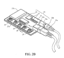
- the electric elements 23 disposed on the board 21 further comprises at least one connector port 25a, 25b, which is connected with at least one connector 22a, 22b respectively to receive/transmit various signals.
- step 13a may be executed to connect the at least one connector 22a, 22b with the at least one connector port 25a, 25b to prevent the second non-solid adhesive with a lower viscosity from permeating through and covering a plurality of connector terminals (not shown) of the at least one connector port 25a, 25b during the application process; otherwise, this would cause failure in normal signal transmissions.
- step 14 is executed to apply the second non-solid adhesive to at least cover the electric elements 23 directly.
- the second non-solid adhesive completely covers the surface of the circuit board 20 other than the button devices 29 to provide a desirable waterproof function.
- the first non-solid adhesive has a higher flexibility than the second non-solid adhesive to allow the button devices 29 to serve the button functions normally.
- the second non-solid adhesive has a lower viscosity than that of the first non-solid adhesive so that the second non-solid adhesive can permeate into the fine slits of the circuit board 21 to seal against water completely.
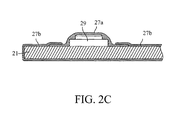
- the second non-solid adhesive only covers the periphery of the first waterproof layer 27a partially and it is necessary to prevent the second non-solid adhesive from covering the first waterproof layer 27a entirely for exposing the first waterproof layer 27a. Because the second waterproof layer 27b formed by the solidified second non-solid adhesive is harder than the first waterproof layer 27a with a higher flexibility, this may prevent a harder second waterproof layer 27b from interfering with the normal operation of the button devices 29.
- the application of the second non-solid adhesive may be accomplished by a brushing or a pouring process. However, in the preferred embodiment, the application of the second non-solid adhesive is accomplished by the pouring process. As shown in FIG. 2D , if the second non-solid adhesive is applied through the pouring process, step 13b needs to be executed before step 14 to put the circuit board 20 into a mould 24.
- the mould 24 may be made of a material selected from the group consisting of polypropylene (PP), polycarbonate (PC), polyurethane (PU), acrylonitrile butadiene styrene (ABS) and nylon.
- the application of the second non-solid adhesive is accomplished in the following way. The second non-solid adhesive with a lower viscosity is poured into the mould 24, and through the natural flow thereof, the second non-solid adhesive is allowed to cover the surface of the plurality of electric elements 23 uniformly without entirely covering the first waterproof layer 27a.
- step 15 is preferably executed ahead to form a vacuum in advance. The purpose is to evacuate the air within the second non-solid adhesive so that the solidified second waterproof layer 27b is adapted to cover the circuit board 20 more closely.
- step 16 is executed where the second non-solid adhesive is solidified in a way similar to that of the first non-solid adhesive, and this will not be further described herein.
- the second non-solid adhesive may be applied only on portions of the circuit board 20 where a waterproof effect is desired, and accordingly, the second waterproof layer 27b formed in step 16 also covers the corresponding portions of the circuit board 20.
- step 17a may be executed corresponding to the aforesaid step 13a.
- step 17a the at least one connector 22a, 22b is disconnected from the at least one connector port 25a, 25b to expose the connector terminals.
- step 13a to connect the connectors 22a, 22b to the connector ports 25a, 25b before the second non-solid adhesive is applied, the solidified second waterproof layer 27b is prevented from covering the connector terminals to adversely affect signal transmissions and result in poor signal quality.
- connector ports 25a, 25b are an earphone jack and a USB connector port respectively, while the connectors 22a, 22b are an earphone plug and a USB connector respectively.
- the circuit board 20 may further have other kinds and another number of connector ports that are adapted to connect with various connectors respectively.
- step 17b shall be executed corresponding to the aforesaid step 13b to remove the circuit board 20, covered with the waterproof layers 27a, 27b, from the mould 24, thus obtaining a circuit board 20 with a waterproof function.
- the first non-solid adhesive applied in this invention shall have a higher flexibility than the second non-solid adhesive so that the first waterproof layer 27a resulting from solidification has an appropriate elasticity, to prevent the waterproof layer from interfering with the action of pressing the button devices 29 due to excessive hardness.
- the second non-solid adhesive shall have a lower viscosity than that of the first non-solid adhesive so that when being applied, the second non-solid adhesive can flow freely on the surface of the circuit board 20 and within gaps between the circuit board 20 and the mould 24 and permeate into all the fine slits of the circuit board 20. In this way, the solidified second waterproof layer 27b can fully serve the waterproof function.
- the first non-solid adhesive of this embodiment should be made of a material comprising silicone, thermoplastics or polyurethane, while the second non-solid adhesive should be made of a material comprising epoxy.
- step 18a is executed to assemble the circuit board 20 to a housing 31, which comprises an upper housing 311 and a lower housing 313, to form the waterproof electronic device 3 of this invention.
- the waterproof electronic device 3 is made to be waterproof, no matter whether the housing 31 has a waterproof function or even if a non-waterproof housing 31 is adopted deliberately in the waterproof electronic device 3 of this invention to reduce costs.
- step 18b may be executed to test if the waterproof electronic device 3 has desirable waterproof properties.
- step 18b places the waterproof electronic device 3 into a pressure vessel (not shown) containing water, which is then sealed and applied with an increased pressure to simulate the case of operating the waterproof electronic device 3 in water.
- the test pressure is set to simulate a pressure that would occur at 50 meters under water and the test lasts for 30 minutes. Finally, the pressure is released and the waterproof electronic device 3 removed from the pressure vessel to inspect for any abnormal conditions and damages of the waterproof mechanism and the operation functions.
- the waterproof test method of this invention is not limited to the method described above. Rather, other test methods will be readily known by those of ordinary skill in the art and may also accomplish the purpose of this invention.
- the waterproof electronic device 3 of this invention formed through the above process comprises a housing 31, a circuit board 20, a first waterproof layer 27a and a second waterproof layer 27b.
- the housing 31 comprises an upper housing 311 and a lower housing 313, and defines a receiving space for the circuit board 20 to be received therein.
- the housing 31 may be a waterproof housing; alternatively, to save costs related to the waterproof measures of the housing, the housing 31 of this invention is preferably permeable to water, i.e., is non-waterproof.
- the circuit board 20 comprises a board 21, a plurality of electric elements 23 and at least one button device 29 (there are five buttons in this embodiment).
- the electric elements 23 and the button device 29 are all disposed on the board 21, and the electric elements 23 comprises at least one connector port (comprises a plurality of connector ports 25a, 25b in this embodiment). Each of the connector ports 25a, 25b has at least one connector terminal for connection with the corresponding external connectors 22a, 22b (as shown in FIG. 2B ). Although only some of the electrical elements are shown by the reference numeral 23 in FIG. 3A , the circuit board 20 further comprises other electrical elements. In addition, even though the connector ports 25a, 25b are an earphone jack and a USB connector port respectively in this embodiment; in other embodiments, the circuit board 20 may further have other kinds and another number of connector ports that are adapted to connect with various connectors respectively.
- the first waterproof layer 27a is formed with the first non-solid adhesive and covers the button device 29 directly.
- the second waterproof layer 27b is formed with the second non-solid adhesive and at least covers the electric elements 23 directly.
- the second waterproof layer 27b covers at least one portion of the connector ports 25a, 25b and leaves the connector terminals exposed. Additionally, as shown in FIG. 2C , the second waterproof layer 27b further covers at least one portion of the first waterproof layer 27a. More specifically, the second waterproof layer 27b covers the periphery of the first waterproof layer 27a and leaves portions of the first waterproof layer 27a corresponding to the button device 29 exposed.
- the first non-solid adhesive has a higher flexibility than the second non-solid adhesive so that the first waterproof layer 27a resulting from solidification has an appropriate elasticity.
- the second non-solid adhesive has a lower viscosity than that of the first non-solid adhesive, so the second non-solid adhesive can fully permeate into all fine slits of the circuit board 20, thus forming a second waterproof layer 27b that can provide an adequate waterproof effect.
- the first non-solid adhesive is preferably made of a material comprising silicone, thermoplastics or polyurethane
- the second non-solid adhesive is preferably made of a material comprising epoxy.
- the second waterproof layer 27b directly covers the board 21, the plurality of electric elements 23 and the connector ports 25a, 25b of the circuit board 20, but leaves the connector terminals exposed to facilitate the subsequent connection with the connectors 22a, 22b during use. It should be noted herein that the connector terminals within the connector ports 25a, 25b are not covered by the second waterproof layer 27b to prevent interference with the electrical connection between the connectors 22a, 22b and the connector terminals.
- the waterproof electronic device 3 may be a multimedia player (e.g., a MP3 player) in this embodiment; however, as will be readily appreciated by those of ordinary skill in the art, the waterproof electronic device 3 may also be any of various other electronic devices, such as a digital camera, a light emitting device, a mobile phone and so on. Furthermore, the waterproof electronic device 3 of this embodiment may not comprise the housing 31, but may be used or disposed directly in other devices. The way in which the waterproof electronic device 3 is formed is just as described above in the embodiment of the waterproof method, and thus will not be further described herein.
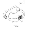
- the waterproof electronic device of this invention may also be disposed in a strap-like structure such as a strap of a diving mask. As shown in FIG. 4 , the waterproof electronic device of this invention is disposed in a diving mask 4, in which a strap 41 of the diving mask 4 is used as a housing of the waterproof electronic device. In this embodiment, the circuit board 20 covered with the waterproof layers 27a, 27b is received in the strap 41.
- this invention provides a waterproof method for an electronic device and a waterproof electronic device formed by the method to replace the conventional solutions of either using an additional waterproof housing or disposing a waterproof gasket in the electronic device.
- this invention makes an improvement by making the electronic device waterproof while still having a light weight, small volume and low cost.
- waterproof layers of different properties are formed in the waterproof method of this invention, which makes the electronic device more convenient to use in practical applications.
Landscapes
- Engineering & Computer Science (AREA)
- Manufacturing & Machinery (AREA)
- Microelectronics & Electronic Packaging (AREA)
- Casings For Electric Apparatus (AREA)
- Telephone Set Structure (AREA)
Applications Claiming Priority (2)
| Application Number | Priority Date | Filing Date | Title |
|---|---|---|---|
| TW97116979 | 2008-05-08 | ||
| US12/419,514 US20090279269A1 (en) | 2008-05-08 | 2009-04-07 | Waterproof method for electronic device and waterproof electronic device |
Publications (2)
| Publication Number | Publication Date |
|---|---|
| EP2117024A2 true EP2117024A2 (fr) | 2009-11-11 |
| EP2117024A3 EP2117024A3 (fr) | 2010-12-01 |
Family
ID=41087382
Family Applications (1)
| Application Number | Title | Priority Date | Filing Date |
|---|---|---|---|
| EP09157960A Withdrawn EP2117024A3 (fr) | 2008-05-08 | 2009-04-15 | Procédé imperméable d'un dispositif électronique et dispositif électronique imperméable |
Country Status (2)
| Country | Link |
|---|---|
| US (1) | US20090279269A1 (fr) |
| EP (1) | EP2117024A3 (fr) |
Cited By (1)
| Publication number | Priority date | Publication date | Assignee | Title |
|---|---|---|---|---|
| EP3043201A3 (fr) * | 2015-01-06 | 2016-09-28 | Seiko Epson Corporation | Dispositif d'affichage d'image |
Families Citing this family (6)
| Publication number | Priority date | Publication date | Assignee | Title |
|---|---|---|---|---|
| CA2785007C (fr) | 2009-12-21 | 2018-02-06 | Nestec S.A. | Identification de capsules contenant un ingredient de boisson |
| US8155717B1 (en) * | 2010-02-02 | 2012-04-10 | Marcus Watson | Cellular phone casing and associated method |
| JP5693515B2 (ja) * | 2012-01-10 | 2015-04-01 | エイチズィーオー・インコーポレーテッド | 内部耐水性被覆を備える電子デバイス |
| ES2700853T3 (es) * | 2015-12-01 | 2019-02-19 | Friwo Geraetebau Gmbh | Cubierta impermeable, suministro de energía y método de montaje |
| CN105430932A (zh) * | 2015-12-16 | 2016-03-23 | 小米科技有限责任公司 | 带保护电路板及其制作方法和装置 |
| US20180308222A1 (en) * | 2016-10-17 | 2018-10-25 | Jack Wade | Enhanced electronic dive mask system |
Family Cites Families (3)
| Publication number | Priority date | Publication date | Assignee | Title |
|---|---|---|---|---|
| US4913285A (en) * | 1987-03-09 | 1990-04-03 | Alps Electronic Co., Ltd. | Water-and-dust-proof push-button switch housing dummy terminal for air venting |
| JPH0644178U (ja) * | 1992-11-13 | 1994-06-10 | 株式会社小糸製作所 | 回路基板 |
| US7264992B2 (en) * | 2004-08-06 | 2007-09-04 | Paul Hsueh | Removable flash integrated memory module card and method of manufacture |
-
2009
- 2009-04-07 US US12/419,514 patent/US20090279269A1/en not_active Abandoned
- 2009-04-15 EP EP09157960A patent/EP2117024A3/fr not_active Withdrawn
Cited By (1)
| Publication number | Priority date | Publication date | Assignee | Title |
|---|---|---|---|---|
| EP3043201A3 (fr) * | 2015-01-06 | 2016-09-28 | Seiko Epson Corporation | Dispositif d'affichage d'image |
Also Published As
| Publication number | Publication date |
|---|---|
| US20090279269A1 (en) | 2009-11-12 |
| EP2117024A3 (fr) | 2010-12-01 |
Similar Documents
| Publication | Publication Date | Title |
|---|---|---|
| EP2117024A2 (fr) | Procédé imperméable d'un dispositif électronique et dispositif électronique imperméable | |
| CN101583247B (zh) | 用于电子装置的防水方法及防水电子装置 | |
| TWI384920B (zh) | 用於電子裝置之防水方法及防水電子裝置 | |
| US8925195B2 (en) | Methods for forming sealed connectors for portable electronic devices | |
| US8506327B2 (en) | Portable electronic devices with sealed connectors | |
| US8625290B2 (en) | Waterproof structure for portable terminal | |
| EP2779319B1 (fr) | Prise de jack d'écoute imperméable à l'eau et son procédé de fabrication | |
| CN207802134U (zh) | 一种电子设备 | |
| TWI424602B (zh) | 防水電池 | |
| KR20110041384A (ko) | 휴대용 단말기의 방수 구조 | |
| JP4162674B2 (ja) | フレキシブル配線基板及び電子機器 | |
| KR20110084359A (ko) | 기판접속 커넥터의 방수부착구조 | |
| CA2737926C (fr) | Carte de circuits imprimes surmoulee | |
| EP2461548B1 (fr) | Dispositif de communication | |
| CN207354541U (zh) | 一种防水麦克风模组 | |
| US8664656B1 (en) | Devices and methods for embedding semiconductors in printed circuit boards | |
| KR101892132B1 (ko) | 휴대 단말기에서 이어 잭 방수 장치 | |
| US7963786B1 (en) | Audio jack | |
| CN110265811B (zh) | 耳机连接器、移动终端及耳机连接器的制作工艺 | |
| JP4966620B2 (ja) | 電子機器 | |
| KR101407498B1 (ko) | 기판용 테이프의 이형필름 구조체 | |
| US9659723B2 (en) | Accessory controller with switch module | |
| CN201556771U (zh) | 防水插座模块 | |
| JP2010135740A (ja) | 配線体、シール構造及び電子機器 | |
| CN102510697B (zh) | 一种电子产品外接线防水结构及其装配方法 |
Legal Events
| Date | Code | Title | Description |
|---|---|---|---|
| PUAI | Public reference made under article 153(3) epc to a published international application that has entered the european phase |
Free format text: ORIGINAL CODE: 0009012 |
|
| AK | Designated contracting states |
Kind code of ref document: A2 Designated state(s): AT BE BG CH CY CZ DE DK EE ES FI FR GB GR HR HU IE IS IT LI LT LU LV MC MK MT NL NO PL PT RO SE SI SK TR |
|
| PUAL | Search report despatched |
Free format text: ORIGINAL CODE: 0009013 |
|
| AK | Designated contracting states |
Kind code of ref document: A3 Designated state(s): AT BE BG CH CY CZ DE DK EE ES FI FR GB GR HR HU IE IS IT LI LT LU LV MC MK MT NL NO PL PT RO SE SI SK TR |
|
| 17P | Request for examination filed |
Effective date: 20110601 |
|
| STAA | Information on the status of an ep patent application or granted ep patent |
Free format text: STATUS: THE APPLICATION IS DEEMED TO BE WITHDRAWN |
|
| 18D | Application deemed to be withdrawn |
Effective date: 20121101 |