EP2119329B1 - Dispositif et procédé d'assemblage de blocs optoélectroniques - Google Patents
Dispositif et procédé d'assemblage de blocs optoélectroniques Download PDFInfo
- Publication number
- EP2119329B1 EP2119329B1 EP08735161A EP08735161A EP2119329B1 EP 2119329 B1 EP2119329 B1 EP 2119329B1 EP 08735161 A EP08735161 A EP 08735161A EP 08735161 A EP08735161 A EP 08735161A EP 2119329 B1 EP2119329 B1 EP 2119329B1
- Authority
- EP
- European Patent Office
- Prior art keywords
- circuit board
- printed circuit
- board surface
- optical
- optoelectronic component
- Prior art date
- Legal status (The legal status is an assumption and is not a legal conclusion. Google has not performed a legal analysis and makes no representation as to the accuracy of the status listed.)
- Not-in-force
Links
Images


Classifications
-
- G—PHYSICS
- G02—OPTICS
- G02B—OPTICAL ELEMENTS, SYSTEMS OR APPARATUS
- G02B6/00—Light guides; Structural details of arrangements comprising light guides and other optical elements, e.g. couplings
- G02B6/24—Coupling light guides
- G02B6/42—Coupling light guides with opto-electronic elements
- G02B6/4201—Packages, e.g. shape, construction, internal or external details
- G02B6/4246—Bidirectionally operating package structures
-
- G—PHYSICS
- G02—OPTICS
- G02B—OPTICAL ELEMENTS, SYSTEMS OR APPARATUS
- G02B6/00—Light guides; Structural details of arrangements comprising light guides and other optical elements, e.g. couplings
- G02B6/24—Coupling light guides
- G02B6/42—Coupling light guides with opto-electronic elements
- G02B6/4201—Packages, e.g. shape, construction, internal or external details
- G02B6/4204—Packages, e.g. shape, construction, internal or external details the coupling comprising intermediate optical elements, e.g. lenses, holograms
-
- H—ELECTRICITY
- H05—ELECTRIC TECHNIQUES NOT OTHERWISE PROVIDED FOR
- H05K—PRINTED CIRCUITS; CASINGS OR CONSTRUCTIONAL DETAILS OF ELECTRIC APPARATUS; MANUFACTURE OF ASSEMBLAGES OF ELECTRICAL COMPONENTS
- H05K1/00—Printed circuits
- H05K1/02—Details
- H05K1/14—Structural association of two or more printed circuits
- H05K1/144—Stacked arrangements of planar printed circuit boards
-
- H—ELECTRICITY
- H05—ELECTRIC TECHNIQUES NOT OTHERWISE PROVIDED FOR
- H05K—PRINTED CIRCUITS; CASINGS OR CONSTRUCTIONAL DETAILS OF ELECTRIC APPARATUS; MANUFACTURE OF ASSEMBLAGES OF ELECTRICAL COMPONENTS
- H05K1/00—Printed circuits
- H05K1/18—Printed circuits structurally associated with non-printed electric components
- H05K1/182—Printed circuits structurally associated with non-printed electric components associated with components mounted in printed circuit boards [PCB], e.g. insert-mounted components [IMC]
-
- H—ELECTRICITY
- H05—ELECTRIC TECHNIQUES NOT OTHERWISE PROVIDED FOR
- H05K—PRINTED CIRCUITS; CASINGS OR CONSTRUCTIONAL DETAILS OF ELECTRIC APPARATUS; MANUFACTURE OF ASSEMBLAGES OF ELECTRICAL COMPONENTS
- H05K2201/00—Indexing scheme relating to printed circuits covered by H05K1/00
- H05K2201/10—Details of components or other objects attached to or integrated in a printed circuit board
- H05K2201/10007—Types of components
- H05K2201/10121—Optical component, e.g. opto-electronic component
Definitions
- the present invention relates to devices and methods for the construction of optoelectronic assemblies, as they can be used for example in optical transceivers.
- optical transceivers For transmission of optical signals over optical fiber networks cost-effective optical transceivers are needed to couple the optical signals, in particular light, in the optical fiber lines or to receive from the fiber lines. Due to their high transmission capacity, the demand for optical transmission systems is steadily increasing, which makes inexpensive optoelectronic systems necessary.
- optoelectronic low-cost systems in particular optical transceivers
- leadframes as chip carriers
- surface-active components such as surface emitting light or laser diodes or photodiodes
- Surface-active optical components have an optically active surface, via which light can be radiated or received perpendicular to the plane of the component.
- edge-active optical components In contrast, in the case of edge-active optical components, the light can emerge or enter at one or two flanks of the component.
- edge-active components such as edge-emitting lasers
- TO transistor outline canister
- a complex butterfly housing is typically used.
- Chip-on-board technology is a production technology in which bare semiconductors or integrated circuits are glued directly onto a printed circuit board and then connected with micro wires to the printed circuit board.
- edge-active and surface-active components for example laser and photodiodes
- optical transceivers For a cost-effective implementation of optoelectronic products, in particular optical transceivers, but would be a mixed structure of optical components of different component height, which are applied both in chip-on-board technology and in TO-Can technology on printed circuit boards and the optically active end surfaces in a level, desirable. If the end faces of all optically active components are mounted at the same height in an optoelectronic module, then, for example, an optical plug can be connected in a simple manner to the optoelectronic module.
- the US 2004/0033029 A1 shows a module with a transparent base layer into which a fiber line is introduced.
- a transparent base layer On the transparent base layer, two laterally offset laser diodes are applied by means of transparent adhesive in a layer stack. The two lasers are laterally spaced by the distance d, so that different wavelengths can be coupled into the fiber line.
- the citation does not describe exactly how the laser diodes or their substrates (which could be interpreted as circuit board surfaces) are implemented.
- the US 5,857,054 describes an apparatus and method for removably attaching one or more optical fibers to be in alignment with a corresponding electro-optic component on a circuit board within an enclosure.
- the lid is attached to an aperture of a sheath, thereby protecting the circuit board from dust and liquids.
- the lid and the protective sheath are on an integral unit.
- the invention allows one or more optical fibers to be removably attached to a first side of a lid or enclosure, and a circuit board having one or more electro-optic components positioned precisely thereon to be attached to and through the other side thereof the attached fiber to be accessed through a through hole in the lid.
- a sleeve surrounds at least one optical fiber in the vicinity of one end thereof and includes a seat surface which sits on the outside of the lid or cover / sheath.
- the WO 02/12942 A1 discloses an apparatus or array of arrayed optical subassemblies comprising modular units called single channel subassemblies.
- Each of the one-channel subassemblies includes a small format optical subassembly attached to a substrate and an optical coupling element, all of which are connected to a base.
- the optical coupling element comprises a focusing element and a sleeve receiving bore.
- the arranged device makes it possible to remove one of the one-channel sub-arrays or to exchange it with another one-channel subarray.
- the small-format optical subarray of the one-channel subassembly may be a transmitter or a receiver.
- the device is a modular, high density multi-optic transceiver array.
- the KR 1020040025202 discloses a bidirectional optical transceiver module that uses a single-mode fiber and a carrier of an optical waveguide used therein that are provided to enable the implementation of passive alignment.
- an optical waveguide has a mirror, an optical filter, and a core, which provides an optical path of transmitted and received light.
- a carrier of an optical waveguide is combined with the optical waveguide and connected to an optical cable.
- a module embedded in an optical device is embedded with a light emitting device and a photodetector.
- the first combination part combines the optical waveguide and the carrier of the optical waveguide at a fixed position to align the core and the optical fiber where light transmission and reception to each other is possible.
- the second combination part combines the support of the optical waveguide and the module embedded in the optical element at a fixed position to the core and the Align light emitting device and the photodetector, where a light transmission and reception to each other is possible.
- the FR 2 890 456 discloses an apparatus for hermetically sealed coupling between an optoelectronic component emitting and / or receiving a light beam and an optical transmitter which transports the light beam.
- the hermetic coupling device has a substrate provided with a blind hole with a base wall, with a part of the optical transmitter being inserted.
- the substrate is formed by a stack of a first layer and a second layer.
- the light beam passes through the base wall of the blind hole, the substrate receiving the opto-electronic component substantially opposite the blind hole. Reflection patterns are interposed between the two layers of the hermetic coupling device substantially at the periphery of the dummy hole and the reflection part of the light beam emitted by the opto-electronic component.
- a module consists of a miniature printed circuit board; Parts are mounted on one face of the board, and other parts that are large, at least in terms of mounting height, are mounted on the other face. Pads are formed on the circumference of the other surface.
- a main printed circuit board has a small rectangular hole similar to and smaller than the miniature printed circuit board. Pads are formed on the circumference of the rectangular hole. The high parts are inserted in the rectangular hole and the module is superimposed on the main printed circuit board. Pads on both the module and the printed motherboard are with connected by soldering and thus the former is attached to the latter.
- the US 6,125,041 describes a card-type electronic device including at least one circuit board, the circuit board including a sub-mounting portion partially surrounded by a cutout portion and mechanically and electrically connected to another portion of the circuit board via a flexible support portion.
- the flexible support portion is bent so that a height position of the part attachment portion is different from a height position of a remaining portion of the circuit board.
- the US2003016920 describes an optical transmission jack module which, on a holder body in which a specified connector is to be inserted, comprises an optical semiconductor device for inputting and outputting an optical signal via the connector.
- the optical semiconductor device is constructed such that a light-emitting chip and a light-receiving chip are mounted on a one-side surface of a lead frame in which the light-emitting chip and the light-receiving chip are integrally molded with a translucent resin.
- the surface of the lead frame is inclined with respect to a center hole of the inserted plug.
- the US 2001/000031611 describes an optical system unit for an optical transceiver having a transmitting lens and a receiving lens, which are formed as bent protrusions of an optical transparent resin material, wherein the distal ends of the arcuate protrusions each before an end of an optical fiber for transmitting and an end of an optical fiber for receiving, which are arranged at a certain distance from each other and housed in a single fiber optic cable, wherein a lead frame is provided in the optically transparent resin material and is formed by bending so that it has two stages, the distances of the two stages along the axes of the optical fibers from the one end of the optical fiber for transmission and the one end of the optical fiber for reception are different from each other, and a light-emitting device in the optically transparent resin ma and disposed on a step of the lead frame so as to face the one end of the optical fiber for transmission, and a light receiving device provided in the optically transparent resin material and disposed on the other step of the lead frame so as to be connected to one end of the lead
- the object of the present invention is thus to provide apparatus and methods for providing optoelectronic modules having a mixed structure of first optical components with a first height and second optical components with a second height different from the first.
- the present invention is based on the finding that optically active end faces of optical components with a low overall height and optically active end faces of components with a higher overall height can be brought into at least approximately the same plane by mounting the optical components of low overall height on a first printed circuit board surface can be located over a second board surface on which the optical components are mounted with the higher height.
- the higher optical components of the second, lower-lying printed circuit board surface may in this case protrude completely or partially into the overlying first printed circuit board surface, if appropriate recesses or openings are provided therein.
- optical components can thus be mounted on different, substantially in parallel one above the other or one behind the other PCB surfaces.
- the optical components can be positioned on the different circuit board surfaces in the normal direction to each other.
- the normal direction means a direction of a common normal of the printed circuit board surfaces lying essentially parallel one above the other or one behind the other.
- an optical transparency of the printed circuit board surfaces can be ensured by means of suitable windows, which in the simplest case consist of holes or openings in the printed circuit board surfaces.
- optics can also be embedded in a printed circuit board surface in order to ensure optical transparency through the printed circuit board surface.
- a printed circuit board or printed circuit board surface can also be designed completely or partially transparent according to comparative examples.
- One advantage of the present invention is that different packaged and unhoused optoelectronic components can be used together in an optoelectronic module and an arrangement of the optical components relative to one another in the normal direction (eg alignment of the optically active surfaces at the same height in the normal direction can be ensured can enable a cost-effective production of an optoelectronic module despite the use of optical components with different heights and construction techniques.
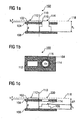
- Fig. 1a 1 shows a device 100 having a first optical component 102 on a first printed circuit board surface 104 and a second optical component 106 on a second printed circuit board surface 108, according to one exemplary embodiment of the present invention.
- the first printed circuit board surface 104 and the second printed circuit board surface 108 are arranged substantially parallel to one another behind one another or one above the other so that the first printed circuit board surface 104 and the second printed circuit board surface 108 point in a same normal direction 110.
- Both the first optical component 102 and the second optical component 106 can each be optically coupled to an optical interface located behind or above the first 104 and second printed circuit board surface 108 in the normal direction 110.
- the optical interface is formed, for example, by the entrance surface of a waveguide or by the entrance surfaces of several waveguides, including, for example, as a waveguide for incoming information, ie as a receiving fiber, and as a waveguide for outward information, ie as a transmitting fiber acts.
- the optical coupling means for example, that both a surface of the first optical component 102 and a surface of the second optical component 106 can reach from the optical interface and vice versa.
- the first optical component 102 has an optically active end or surface 112 and the second optical component 106 has an optically active end or surface 114.
- the optically active surfaces 112, 114 are light entry and / or light exit surfaces.
- the optically active surface is, for example, a glass window from which a laser beam of an edge-emitting laser can emerge.
- Photodiode is an optically active surface formed by PN-doped semiconductor material or a PN junction.
- the first printed circuit board surface 104 and / or the second printed circuit board surface 108 is at least partially optically transparent to both the first optical component 102 and the second optical component 106 with the optical interface lying in the normal direction 110 behind the first 104 and second printed circuit board surface 108 to pair optically.
- this also means that optical components mounted on the lower printed circuit board surface 108 can receive light from an optical interface above the first printed circuit board surface 104 or can transmit light through the first printed circuit board surface 104 to an optical interface located behind it.
- the printed circuit board surfaces 104, 108 may have openings for respective underlying optical components.
- optical components of lower printed circuit board surfaces may protrude completely or partially into the overlying printed circuit board surfaces, as shown by way of example in FIG Fig. 1a is shown for the second optical component 106, which projects through an opening 116 in the first circuit board surface 104 beyond the same.
- first optical components 102 having a first optically active surface 112 at a first height h 1 from the first printed circuit board surface 104 and second optical components 106 with a second optically active surface 114 at a second height h 2 of the second circuit board surface 108, wherein the first height h 1 is smaller than the second height h 2 , can be arranged so that the first optically active component surface 112 and the second optically active component surface 114 lie substantially in a common plane 118.
- the first optical device 102 could be, for example, a photodiode deposited on the first printed circuit board surface 104 using the chip on-board technique
- the second optical device 106 on the second printed circuit board surface 108 could be one constructed by the TO-Can technique Be a laser.
- the opening 116 in the first printed circuit board surface 104 for example, an edge-emitting laser diode of the laser 106 with a much higher height than the photodiode 102 can be installed.
- the laser 106 is soldered, for example, on the second circuit board surface 108.
- the position of the optical components 102 and 106 or of the optically active component surfaces 112 and 114 can be changed relative to one another so that both optically active component surfaces 112, 114 lie on the desired common reference plane 118 to position, for example, a receptacle for an optical connector.
- the first circuit board surface 104 which represents a frontmost or uppermost board surface
- the photodiode 102 is constructed on this circuit board surface 104, the laser 106 in TO-Can technology can be positioned, for example, by a plastic part at a correct height on the second circuit board surface 108.
- the device or assembly can be housed or encapsulated with plastic, for example.
- FIG. 1a A top view of in Fig. 1a shown in a side view device 100 according to an embodiment of the present invention is in Fig. 1b shown.
- Fig. 1b shows the first and upper printed circuit board surface 104, to which the first optical component 102 is applied with the first optically active component surface 112.
- the first circuit board surface 104 has the opening 116 for the second optical component 106 mounted on the lower circuit board surface 108 (not shown).
- the second component 106 projects through the opening 116 through the first printed circuit board surface 104, as a result of which the optically active component surface 114 of the second component 106 becomes optically accessible from an optical interface above the drawing plane.
- the apparatus 100 can be coupled to the first circuit board surface 104 and the reference plane 118, in which the two optically active device surfaces 112, 114, for example, an optical fiber line.
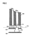
- This may be, for example, a blunt coupling, as shown schematically in FIG Fig. 2 is shown.
- the fiber line accommodates a plurality of juxtaposed internal waveguides or fibers, as also exemplified in Fig. 2 is shown.
- one optical fiber may be provided for one optical component and another for the other optical component. Contrary to the example of Fig. 2 but it would also be possible that a fiber is coupled to both optical components.
- Fig. 2 schematically shows the basis of Fig. 1a, b described device to which an optical fiber line 200 is coupled. It is in the in Fig. 2
- the optical fiber line 200 in the reference plane 118 in which the two optically active component surfaces 112 and 114 are located, is butt-coupled to the two components 102 and 106.
- fiber optic face may be faced on one side and optical components 106 and 102 on the other side across a gap.
- the gap can be also missing, in which case face and optical components lie directly on top of each other.
- an end face of the fiber 200 and in particular, the input / output faces of individual internal fibers 200a and 200b in the optical fiber line 200 on the one hand and the optically active device surfaces 112, 114 on the other hand are directly opposite to be optically coupled.
- the first component 102 may be a photodiode as optical receiver and the second optical component 106 may be an optical transmitter in the form of an edge-emitting laser.
- An optical receiver generally serves to receive light power from the optical fiber 200 and to convert the received light power into electrical signals.
- the optical transmitter serves to convert electrical signals into light power, which can be coupled into the fiber 200 via an optically active component surface.
- the fiber 200a serves as a transmitting fiber and the fiber 200b as a receiving fiber.
- only one fiber could be provided inside the fiber line coupled to both optical components for both transmission and reception.
- optics in the form of e.g. Lens or lens arrays are mounted to improve an optical coupling efficiency between device 100 and optical fiber 200.
- the optically active component surfaces 112, 114 can also lie in different planes, as shown by way of example in FIG Fig. 1c is shown.
- the second optically active device surface 114 of the second optical component 106 below and behind the first circuit board surface 104 it has, in order to ensure optical transparency, a transparent point 220 in order to make the second optically active component surface 114 for an optical interface above the first printed circuit board surface 104 optically accessible.
- the optically transparent point or recess 220 may be a simple hole opening or else an optic embedded in the circuit board surface 104 or applied to the circuit board surface 104 in the form of a transparent plane or, for example, a lens.
- the transparent area 220 is, for example, a lens with a first focal plane in the reference plane 118 and a second focal plane in which the second optically active component area 114 is located, then it is also possible to use the lens in FIG Fig. 1c shown example, an optical transceiver for coupling to an optical fiber can be realized.
- the optically active component surfaces 112, 114 thus have a defined height difference ⁇ h with respect to the normal direction 110.
- the first printed circuit board surface 104 and the second printed circuit board surface 108 to be arranged at a predefined distance d to each other.
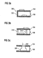
- Fig. 3a shows a side view of a U-shaped printed circuit board 300 having a first printed circuit board surface 104 and a second printed circuit board surface 108.
- the two printed circuit board surfaces 104, 108 are held by a third printed circuit board surface 302 of the printed circuit board 300 at a predefined distance d to each other.
- the third circuit board surface 302 is not vertical to the two circuit board surfaces 104 and 108 must run, but also different than in Fig. 3a represented, can arranged.
- the third printed circuit board surface 302 could have an arcuate shape, which can be created, for example, by bending the printed circuit board 300.
- the embodiment shown is a suitably bent flexible printed circuit board 300, which has two substantially parallel printed circuit board sections with printed circuit board surfaces 104, 108.
- the bending may, for example, have been achieved by means of rigid-flex technology, and the printed circuit board thus bent may be held, for example, at the side opposite the bending edge by a plug which is used for the electrical connection to the opto-electronic components and any other components on the PCB serves.
- the first printed circuit board surface 104 and the second printed circuit board surface 108 are therefore formed by mutually opposite outer surfaces of the curved printed circuit board 300.
- the printed circuit board 300 can be equipped on both sides, i. Components may be mounted on top and / or bottom of circuit board surfaces 104, 108.
- Fig. 3b shows a first circuit board with a first circuit board surface 104 and a second circuit board with a second circuit board surface 108, wherein the two circuit boards are separate circuit boards.
- suitable spacers 310 may be provided between the circuit board surfaces 104, 108, as well as in Fig. 3b is indicated.
- Fig. 3c shows two printed circuit board surfaces 104, 108 of separate printed circuit boards, which are held by a mounted on the lower or rear circuit board surface 108 component 320 at the predefined distance d substantially parallel to each other.
- the first printed circuit board or the first printed circuit board surface 104 may be plugged or glued onto a surface 322 of the component 320, for example.
- a soldering of the component surface 322 with the circuit board surface 104 is equally conceivable.
- the component surface 322 is an optically active component surface, the region of the printed circuit board surface 104 lying above the optically active surface 322 will be made transparent.
- the possibilities already described above transparent glass surface, lens, etc.
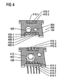
- Fig. 4 shows a perspective view of two separate circuit boards 400 and 402.
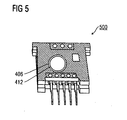
- the first printed circuit board 400 has on a first printed circuit board surface 104 a photodiode 404 applied in chip-on-board technology. Furthermore, a circular opening 406 is made in the first circuit board 400. Furthermore, the first circuit board 400 has five receptacles 408-1 to 408-5 for spacer pins. On an opposite side, the first circuit board 400 further three receptacles 410-1 to 410-3 for more spacer pins.
- the second printed circuit board 402 has on a second printed circuit board surface 108 a laser 412 in TO-Can technology. Further, the second circuit board 402 five spacer pins 414-1 to 414-5, which can engage with their ends in the receptacles 408-1 to 408-5 of the first circuit board 400. Second spacer pins 416-1 to 416-3 can engage with their ends in the receptacles 410-1 to 410-3 of the first printed circuit board 400 provided for this purpose.
- the optically active surface of the laser 412 passes through the designated circular opening 406, whereby the optically active surface of the laser 412 and the optically active surface of the photodiode 404 are at least approximately in one plane.
- the spacer pins 414-1 to 414-5, 416-1 to 416-3 can be soldered to the receptacles 408-1 to 408-5, 410-1 to 410-3 provided for this purpose, for example. so that's in Fig. 5 shown opto-electronic transmission / reception module 500 with realized in different construction technology laser 412 and photodiode 404 results.
- Fig. 6a and 6b show a further embodiment of an apparatus for optical coupling to a fiber line, wherein Fig. 6a shows the coupled state and Fig. 6b only a plan view of the PCB order shows.
- the printed circuit boards 104 and 108 are arranged one behind the other in a housing 600 having a receptacle 602 for a plug connection with one end of the fiber line 200.
- a plug 604 is provided, which mates with the receptacle 602 of the housing 600, to fit snugly into the receptacle 602.
- the receptacle may also be provided at the fiber end.
- a suitable device may be provided which is an accidental one Prevent extraction of the fiber line 200 from the receptacle, such as a latch.
- the fiber line 200 In the inserted state of the fiber line 200, for example, it is at a predetermined distance from the front sides of the optical components, which may also be zero.
- an optical device 606 such as a lens or other beam shaping device.
- the printed circuit boards 104 and 108 are spaced apart from each other in the housing 600 such that the exit surface of the optical device 606 and one surface of the laser 106 lie in a plane 610 opposite the end face of the fiber line 200 in the case where it is inserted is.
- Fig. 6a and 6b It can be seen that other electrical components 612 can also be arranged on the rear side of the printed circuit board 108, and that an electrical plug which can have conductor pieces held by a plastic part 614 can at least partially contribute to the fact that the printed circuit boards 104 and 108 show their mutual position keep their mutual distance. The latter will be in Fig. 6b exemplarily achieved by the component 106.
- the electrical connector with the plastic spacer 614 may include electrical conductors 616, which may be embodied as pins for insertion into corresponding sockets on the printed circuit boards 104 and 108 or as sockets for receiving corresponding pins on the printed circuit boards 104 and 108.
- Spacers 618 can be seen, which can also serve as electrical interconnections between components on the under defencelicen printed circuit boards 104 and 108.
- the present invention comprises a method for arranging a first printed circuit board surface with a first optical component and a second A printed circuit board surface having a second optical component, such that the first and second circuit board surfaces are arranged substantially parallel to one another, such that the first circuit board surface and the second circuit board surface point in a same normal direction, and so that both the first optical component and the second optical component can be coupled in a lying in the normal direction behind the first and second circuit board surface optical interface.
- the exemplary embodiments have been described in the foregoing by way of example only with reference to two printed circuit board surfaces arranged one above the other or one behind the other.
- An arrangement of more than two superimposed one another or one behind the other substantially parallel to each other PCB surfaces is of course also conceivable, if it requires a corresponding application. This can be the case, for example, if more than two optical components, each with a different component height, are to be installed in an optoelectric module.
- Embodiments of the present invention enable a cost-effective construction technique, for example for optical transceivers, with which it is possible to obstruct optical components of different component height, but which require a defined adjustment of optically active component surfaces in the normal direction, as for example in opto-electrical hybrid constructions as a combination of TO -Can technology and chip-on-board technology may be the case.
- optically active device surfaces of optical components can be mounted in the same height in a module in order to be able to easily connect, for example, an optical plug to the module.
- This is according to embodiments by a defined distance d of printed circuit boards or printed circuit board surfaces on which the optical components of different Component height are mounted reached.
- Embodiments of the present invention make it possible, despite a difference in height, to use surface-active chip-on-board components (eg photodiodes) as well as edge-active TO-can components (eg lasers) in an opto-electrical module and at the same time all optical components at the same height or to arrange in a defined height difference .DELTA.h with respect to the normal direction to each other.
- surface-active chip-on-board components eg photodiodes
- edge-active TO-can components eg lasers
Landscapes
- Physics & Mathematics (AREA)
- General Physics & Mathematics (AREA)
- Optics & Photonics (AREA)
- Engineering & Computer Science (AREA)
- Microelectronics & Electronic Packaging (AREA)
- Optical Couplings Of Light Guides (AREA)
Claims (12)
- Dispositif avec
un premier bloc optoélectronique (102) sur une première face de plaque conductrice (104), le premier bloc optoélectronique (102) présentant une première face optiquement active (112) à une première hauteur (h1) à partir de la première face de plaque conductrice (104), et la première face de plaque conductrice (104) présentant une ouverture (116);
un deuxième bloc optoélectronique (106) sur une deuxième face de plaque conductrice (108), le deuxième bloc optoélectronique (106) présentant une deuxième face optiquement active (114) à une deuxième hauteur (h2) à partir de la deuxième face de plaque conductrice (108), la première hauteur étant différente de la deuxième hauteur; et
la première face de plaque conductrice (104) et la deuxième face de plaque conductrice (108) étant disposées l'une derrière l'autre, parallèles entre elles, de sorte que
la première face de plaque conductrice (104) et la deuxième face de plaque conductrice (108) soient orientées dans une même direction normale (110), et
que le premier bloc optoélectronique (102) sur la première face de plaque conductrice (104) soit disposé déplacé latéralement par rapport au deuxième bloc optoélectronique (106), et
la première face de plaque conductrice (104) et la deuxième face de plaque conductrice (108) étant distantes l'une de l'autre de sorte que
le deuxième bloc optoélectronique (106) fasse saillie, à travers l'ouverture (116) dans la première face de plaque conductrice (104), au-delà de cette dernière, et
une première face optiquement active (112) du premier bloc optoélectronique (102) et une deuxième face optiquement active (114) du deuxième bloc optoélectronique (106) se situent dans un plan (118), de sorte que tant le premier bloc optoélectronique (102) que le deuxième bloc optoélectronique (106) puissent être couplés à une interface optique située, dans la direction normale (110), derrière la première et la deuxième face de plaque conductrice, opposée à la première et la deuxième face optiquement active. - Dispositif selon la revendication 1, dans lequel la première face de plaque conductrice (104) et la deuxième face de plaque conductrice (108) sont formées par des surfaces extérieures opposées l'une à l'autre d'une plaque conductrice courbée (300).
- Dispositif selon la revendication 1, dans lequel se trouve, dans le plan (118) ou dans un plan parallèle à ce dernier, une face frontale d'un premier câble à fibre optique (200).
- Dispositif selon l'une des revendications précédentes, dans lequel le premier bloc optoélectronique (102) est placé sur la première face de plaque conductrice (104) à l'aide d'une technique à puce-sur-plaquette.
- Dispositif selon l'une des revendications précédentes, dans lequel le deuxième bloc optoélectronique (106) est placé sur la deuxième face de plaque conductrice (108) à l'aide d'une technique TO-Can.
- Dispositif selon l'une des revendications précédentes, dans lequel le premier bloc optoélectronique (102) est un récepteur optoélectronique.
- Dispositif selon la revendication 6, dans lequel le récepteur optoélectronique présente une photodiode selon la technique à puce-sur-plaquette.
- Dispositif selon l'une des revendications précédentes, dans lequel le deuxième bloc optoélectronique (106) est un émetteur optoélectronique.
- Dispositif selon la revendication 8, dans lequel l'émetteur optoélectronique présente un laser selon la technique TO-Can.
- Système avec
un dispositif selon l'une des revendications 1 à 9; et
un boîtier présentant un dispositif de réception d'une connexion enfichable avec une extrémité d'un câble à fibre (200), la première face de plaque conductrice (104) et la deuxième face de plaque conductrice (108) du dispositif étant placées sur le boîtier de sorte que le câble à fibre soit couplé tant au premier qu'au deuxième bloc optoélectronique. - Ensemble avec un système selon la revendication 10 et un câble à fibre.
- Procédé à l'étape suivante:disposer une première face de plaque conductrice (104) avec un premier bloc optoélectronique (102) présentant une première face optiquement active (112) à une première hauteur (h1) à partir de la première face de plaque conductrice (104), et une ouverture (116) et une deuxième face de plaque conductrice (108) avec un deuxième bloc optoélectronique (106) présentant une deuxième face optiquement active (114) à une deuxième hauteur (h2) à partir de la première face de plaque conductrice (108) qui est différente de la deuxième hauteur, de sorte que la première et la deuxième face de plaque conductrice soient disposées l'une derrière l'autre, parallèles entre elles, de sorte que la première face de plaque conductrice (104) et la deuxième face de plaque conductrice (108) soient orientées dans une même direction normale (110), et que le premier bloc optoélectronique (102) sur la première face de plaque conductrice (104) soit disposé déplacé latéralement par rapport au deuxième bloc optoélectronique (106),et de sorte que la première face de plaque conductrice (104) et la deuxième face de plaque conductrice (108) soient distantes l'une de l'autre de sorte que le deuxième bloc optoélectronique (106) fasse saillie, à travers l'ouverture (116) dans la première face de plaque conductrice (104), au-delà de cette dernière, et une première face optiquement active (112) du premier bloc optoélectronique (102) et une deuxième face optiquement active (114) du deuxième bloc optoélectronique (106) se situent dans un plan (118), de sorte que tant le premier bloc optoélectronique (102) que le deuxième bloc optoélectronique (106) puissent être couplés à une interface optique située, dans la direction normale (110), derrière la première et la deuxième face de plaque conductrice, opposée à la première et la deuxième face optiquement active.
Applications Claiming Priority (2)
| Application Number | Priority Date | Filing Date | Title |
|---|---|---|---|
| DE102007017016A DE102007017016B4 (de) | 2007-04-11 | 2007-04-11 | Optoelektronische Vorrichtung und Verfahren zu deren Aufbau |
| PCT/EP2008/002853 WO2008125278A2 (fr) | 2007-04-11 | 2008-04-10 | Dispositif et procédé d'assemblage de blocs optoélectroniques |
Publications (2)
| Publication Number | Publication Date |
|---|---|
| EP2119329A2 EP2119329A2 (fr) | 2009-11-18 |
| EP2119329B1 true EP2119329B1 (fr) | 2012-02-22 |
Family
ID=39712093
Family Applications (1)
| Application Number | Title | Priority Date | Filing Date |
|---|---|---|---|
| EP08735161A Not-in-force EP2119329B1 (fr) | 2007-04-11 | 2008-04-10 | Dispositif et procédé d'assemblage de blocs optoélectroniques |
Country Status (4)
| Country | Link |
|---|---|
| EP (1) | EP2119329B1 (fr) |
| AT (1) | ATE546981T1 (fr) |
| DE (1) | DE102007017016B4 (fr) |
| WO (1) | WO2008125278A2 (fr) |
Citations (2)
| Publication number | Priority date | Publication date | Assignee | Title |
|---|---|---|---|---|
| US20010000316A1 (en) * | 1999-01-12 | 2001-04-19 | Motoyoshi Kawai | Optical system unit for optical transceiver |
| US20030016920A1 (en) * | 2001-07-23 | 2003-01-23 | Sharp Kabushiki Kaisha | Jack module for optical transmission and plug-and-jack type optical transmission apparatus |
Family Cites Families (12)
| Publication number | Priority date | Publication date | Assignee | Title |
|---|---|---|---|---|
| JPH06334298A (ja) * | 1993-05-27 | 1994-12-02 | Fujitsu Ltd | 表面実装部品の搭載構造 |
| JPH10244791A (ja) * | 1997-03-07 | 1998-09-14 | Fujitsu Ltd | カード型電子装置 |
| US5857054A (en) * | 1997-04-22 | 1999-01-05 | Phoenix International Corporation | Apparatus and method for removably positioning optical fiber to circuit board component in enclosure |
| DE19834090A1 (de) * | 1998-07-29 | 2000-02-03 | Heidenhain Gmbh Dr Johannes | Optoelektronische Sende- und Empfangseinheit |
| US6272271B1 (en) * | 1999-04-29 | 2001-08-07 | General Electric Company | Alignment of optical interfaces for data communication |
| JP4405062B2 (ja) * | 2000-06-16 | 2010-01-27 | 株式会社ルネサステクノロジ | 固体撮像装置 |
| US6416238B1 (en) * | 2000-08-07 | 2002-07-09 | Stratos Lightwave, Inc. | Modular high density multiple optical transmitter/receiver array |
| JP3800135B2 (ja) * | 2002-06-18 | 2006-07-26 | セイコーエプソン株式会社 | 光通信モジュール、光通信モジュールの製造方法および電子機器 |
| US7106973B2 (en) * | 2002-08-13 | 2006-09-12 | Lightpointe Communications, Inc. | Apparatus and method for use in free-space optical communication comprising optically aligned components integrated on circuit boards |
| KR100481578B1 (ko) * | 2002-09-18 | 2005-04-08 | 포테나 옵틱스 코포레이션 | 단일 광섬유를 이용한 양방향 광송수신 모듈 및 그에사용되는 광도파로 거치대 |
| JPWO2006030578A1 (ja) * | 2004-09-14 | 2008-07-31 | 日本電気株式会社 | 集積光部品とその製造方法、及び光通信装置 |
| FR2890456B1 (fr) * | 2005-09-02 | 2009-06-12 | Commissariat Energie Atomique | Dispositif de couplage hermetique |
-
2007
- 2007-04-11 DE DE102007017016A patent/DE102007017016B4/de not_active Expired - Fee Related
-
2008
- 2008-04-10 AT AT08735161T patent/ATE546981T1/de active
- 2008-04-10 EP EP08735161A patent/EP2119329B1/fr not_active Not-in-force
- 2008-04-10 WO PCT/EP2008/002853 patent/WO2008125278A2/fr not_active Ceased
Patent Citations (2)
| Publication number | Priority date | Publication date | Assignee | Title |
|---|---|---|---|---|
| US20010000316A1 (en) * | 1999-01-12 | 2001-04-19 | Motoyoshi Kawai | Optical system unit for optical transceiver |
| US20030016920A1 (en) * | 2001-07-23 | 2003-01-23 | Sharp Kabushiki Kaisha | Jack module for optical transmission and plug-and-jack type optical transmission apparatus |
Also Published As
| Publication number | Publication date |
|---|---|
| WO2008125278A2 (fr) | 2008-10-23 |
| ATE546981T1 (de) | 2012-03-15 |
| WO2008125278A3 (fr) | 2009-05-28 |
| EP2119329A2 (fr) | 2009-11-18 |
| DE102007017016B4 (de) | 2012-02-02 |
| DE102007017016A1 (de) | 2008-10-30 |
Similar Documents
| Publication | Publication Date | Title |
|---|---|---|
| DE10065034B4 (de) | Faseroptikanschluß und Verfahren zum Benutzen desselben | |
| DE69708328T2 (de) | Steckerteil zum direkten ankoppeln optoelektronischer elemente | |
| DE102012200254B4 (de) | Optische Verbindungssysteme mit Stecker, welcher eine optische Biegung hat, und Benutzungsverfahren | |
| DE10105943B4 (de) | Faseroptisches Linsensystem zum Koppeln von Fasern mit oberflächenbefestigten Bauelementen | |
| DE69923894T2 (de) | Optische Baugruppe zum faseroptischen Senden und Empfangen von Daten | |
| DE69907351T2 (de) | Photodiodenmodul | |
| DE68918133T2 (de) | Untereinheiten für hybrid-integrierte optoelektronische Schaltkreise. | |
| EP1249088B1 (fr) | Module de transmission de donnees electro-optique | |
| DE112008003784B4 (de) | Flexible, optische Zwischenverbindung | |
| DE102012207345B4 (de) | Ein aktives optisches Kabel (AOC) mit einem geformten Kunststoff-Leadframe, der einen optischen Stecker überflüssig macht, ein AOC, das den AOC-Stecker integriert, und ein Verfahren zum Verwenden des AOC | |
| DE102010029417A1 (de) | Mittelebenen-montiertes optisches Kommunikationssystem und Verfahren zum Bereitstellen einer Hochdichte-Mittelebenen-Montage von parallelen optischen Kommunikationsmodulen | |
| DE102013214921B4 (de) | Optische Kommunikationssysteme sowie Verfahren zum Hoch-Dichte Montieren von parallelen optischen Kommunikationsmodulen | |
| DE102014103396B4 (de) | Optische Datenkommunikationsmodule mit EMI-Käfig | |
| DE10306044A1 (de) | Wellenleiterbasiertes optisches Koppeln eines Faseroptikkabels und eines optoelektronischen Bauelements | |
| DE10034865A1 (de) | Optoelektronisches oberflächenmontierbares Modul | |
| DE102011006591A1 (de) | Optoelektronisches Transceivermodulsystem | |
| DE102013216589A1 (de) | Verfahren und Systeme zum Blindstecken von multioptischen Faserkonnektormodulen | |
| DE4106721C2 (fr) | ||
| WO2004027482A1 (fr) | Dispositif d'assemblage pour relier de façon liberable au moins un guide d'ondes optiques avec au moins un element optoelectronique et procede pour monter un dispositif d'assemblage de ce type | |
| DE102011004548B4 (de) | Optisches Kommunikationssystem und Verfahren zum Positionieren von parallelen optischen Transceivermodulen in einem optischen Kommunikationssystem | |
| EP2119329B1 (fr) | Dispositif et procédé d'assemblage de blocs optoélectroniques | |
| EP0442312A2 (fr) | Emetteur et/ou récepteur optique intégré | |
| EP1477833B1 (fr) | Dispositif optoélectronique émetteur et/ou récepteur | |
| DE10210359A1 (de) | Optische Kopplung | |
| EP1447696B1 (fr) | Composant optoéléctronique modulaire |
Legal Events
| Date | Code | Title | Description |
|---|---|---|---|
| PUAI | Public reference made under article 153(3) epc to a published international application that has entered the european phase |
Free format text: ORIGINAL CODE: 0009012 |
|
| 17P | Request for examination filed |
Effective date: 20091005 |
|
| AK | Designated contracting states |
Kind code of ref document: A2 Designated state(s): AT BE BG CH CY CZ DE DK EE ES FI FR GB GR HR HU IE IS IT LI LT LU LV MC MT NL NO PL PT RO SE SI SK TR |
|
| 17Q | First examination report despatched |
Effective date: 20100205 |
|
| GRAP | Despatch of communication of intention to grant a patent |
Free format text: ORIGINAL CODE: EPIDOSNIGR1 |
|
| DAX | Request for extension of the european patent (deleted) | ||
| GRAS | Grant fee paid |
Free format text: ORIGINAL CODE: EPIDOSNIGR3 |
|
| GRAA | (expected) grant |
Free format text: ORIGINAL CODE: 0009210 |
|
| RBV | Designated contracting states (corrected) |
Designated state(s): AT BE BG CH CY CZ DK EE ES FI FR GB GR HR HU IE IS IT LI LT LU LV MC MT NL NO PL PT RO SE SI SK TR |
|
| AK | Designated contracting states |
Kind code of ref document: B1 Designated state(s): AT BE BG CH CY CZ DK EE ES FI FR GB GR HR HU IE IS IT LI LT LU LV MC MT NL NO PL PT RO SE SI SK TR |
|
| REG | Reference to a national code |
Ref country code: GB Ref legal event code: FG4D Free format text: NOT ENGLISH |
|
| REG | Reference to a national code |
Ref country code: CH Ref legal event code: EP |
|
| REG | Reference to a national code |
Ref country code: AT Ref legal event code: REF Ref document number: 546981 Country of ref document: AT Kind code of ref document: T Effective date: 20120315 |
|
| REG | Reference to a national code |
Ref country code: IE Ref legal event code: FG4D Free format text: LANGUAGE OF EP DOCUMENT: GERMAN |
|
| REG | Reference to a national code |
Ref country code: DE Ref legal event code: R108 Effective date: 20120208 |
|
| REG | Reference to a national code |
Ref country code: NL Ref legal event code: VDEP Effective date: 20120222 |
|
| LTIE | Lt: invalidation of european patent or patent extension |
Effective date: 20120222 |
|
| PG25 | Lapsed in a contracting state [announced via postgrant information from national office to epo] |
Ref country code: NO Free format text: LAPSE BECAUSE OF FAILURE TO SUBMIT A TRANSLATION OF THE DESCRIPTION OR TO PAY THE FEE WITHIN THE PRESCRIBED TIME-LIMIT Effective date: 20120522 Ref country code: IS Free format text: LAPSE BECAUSE OF FAILURE TO SUBMIT A TRANSLATION OF THE DESCRIPTION OR TO PAY THE FEE WITHIN THE PRESCRIBED TIME-LIMIT Effective date: 20120622 Ref country code: HR Free format text: LAPSE BECAUSE OF FAILURE TO SUBMIT A TRANSLATION OF THE DESCRIPTION OR TO PAY THE FEE WITHIN THE PRESCRIBED TIME-LIMIT Effective date: 20120222 Ref country code: LT Free format text: LAPSE BECAUSE OF FAILURE TO SUBMIT A TRANSLATION OF THE DESCRIPTION OR TO PAY THE FEE WITHIN THE PRESCRIBED TIME-LIMIT Effective date: 20120222 Ref country code: NL Free format text: LAPSE BECAUSE OF FAILURE TO SUBMIT A TRANSLATION OF THE DESCRIPTION OR TO PAY THE FEE WITHIN THE PRESCRIBED TIME-LIMIT Effective date: 20120222 |
|
| PG25 | Lapsed in a contracting state [announced via postgrant information from national office to epo] |
Ref country code: LV Free format text: LAPSE BECAUSE OF FAILURE TO SUBMIT A TRANSLATION OF THE DESCRIPTION OR TO PAY THE FEE WITHIN THE PRESCRIBED TIME-LIMIT Effective date: 20120222 Ref country code: PT Free format text: LAPSE BECAUSE OF FAILURE TO SUBMIT A TRANSLATION OF THE DESCRIPTION OR TO PAY THE FEE WITHIN THE PRESCRIBED TIME-LIMIT Effective date: 20120622 Ref country code: GR Free format text: LAPSE BECAUSE OF FAILURE TO SUBMIT A TRANSLATION OF THE DESCRIPTION OR TO PAY THE FEE WITHIN THE PRESCRIBED TIME-LIMIT Effective date: 20120523 Ref country code: FI Free format text: LAPSE BECAUSE OF FAILURE TO SUBMIT A TRANSLATION OF THE DESCRIPTION OR TO PAY THE FEE WITHIN THE PRESCRIBED TIME-LIMIT Effective date: 20120222 |
|
| REG | Reference to a national code |
Ref country code: IE Ref legal event code: FD4D |
|
| PG25 | Lapsed in a contracting state [announced via postgrant information from national office to epo] |
Ref country code: CY Free format text: LAPSE BECAUSE OF FAILURE TO SUBMIT A TRANSLATION OF THE DESCRIPTION OR TO PAY THE FEE WITHIN THE PRESCRIBED TIME-LIMIT Effective date: 20120222 |
|
| BERE | Be: lapsed |
Owner name: FRAUNHOFER-GESELLSCHAFT ZUR FORDERUNG DER ANGEWAN Effective date: 20120430 |
|
| PG25 | Lapsed in a contracting state [announced via postgrant information from national office to epo] |
Ref country code: SE Free format text: LAPSE BECAUSE OF FAILURE TO SUBMIT A TRANSLATION OF THE DESCRIPTION OR TO PAY THE FEE WITHIN THE PRESCRIBED TIME-LIMIT Effective date: 20120222 Ref country code: SI Free format text: LAPSE BECAUSE OF FAILURE TO SUBMIT A TRANSLATION OF THE DESCRIPTION OR TO PAY THE FEE WITHIN THE PRESCRIBED TIME-LIMIT Effective date: 20120222 Ref country code: RO Free format text: LAPSE BECAUSE OF FAILURE TO SUBMIT A TRANSLATION OF THE DESCRIPTION OR TO PAY THE FEE WITHIN THE PRESCRIBED TIME-LIMIT Effective date: 20120222 Ref country code: CZ Free format text: LAPSE BECAUSE OF FAILURE TO SUBMIT A TRANSLATION OF THE DESCRIPTION OR TO PAY THE FEE WITHIN THE PRESCRIBED TIME-LIMIT Effective date: 20120222 Ref country code: PL Free format text: LAPSE BECAUSE OF FAILURE TO SUBMIT A TRANSLATION OF THE DESCRIPTION OR TO PAY THE FEE WITHIN THE PRESCRIBED TIME-LIMIT Effective date: 20120222 Ref country code: IE Free format text: LAPSE BECAUSE OF FAILURE TO SUBMIT A TRANSLATION OF THE DESCRIPTION OR TO PAY THE FEE WITHIN THE PRESCRIBED TIME-LIMIT Effective date: 20120222 Ref country code: DK Free format text: LAPSE BECAUSE OF FAILURE TO SUBMIT A TRANSLATION OF THE DESCRIPTION OR TO PAY THE FEE WITHIN THE PRESCRIBED TIME-LIMIT Effective date: 20120222 Ref country code: EE Free format text: LAPSE BECAUSE OF FAILURE TO SUBMIT A TRANSLATION OF THE DESCRIPTION OR TO PAY THE FEE WITHIN THE PRESCRIBED TIME-LIMIT Effective date: 20120222 |
|
| PG25 | Lapsed in a contracting state [announced via postgrant information from national office to epo] |
Ref country code: SK Free format text: LAPSE BECAUSE OF FAILURE TO SUBMIT A TRANSLATION OF THE DESCRIPTION OR TO PAY THE FEE WITHIN THE PRESCRIBED TIME-LIMIT Effective date: 20120222 Ref country code: MC Free format text: LAPSE BECAUSE OF NON-PAYMENT OF DUE FEES Effective date: 20120430 Ref country code: IT Free format text: LAPSE BECAUSE OF FAILURE TO SUBMIT A TRANSLATION OF THE DESCRIPTION OR TO PAY THE FEE WITHIN THE PRESCRIBED TIME-LIMIT Effective date: 20120222 |
|
| REG | Reference to a national code |
Ref country code: CH Ref legal event code: PL |
|
| PLBE | No opposition filed within time limit |
Free format text: ORIGINAL CODE: 0009261 |
|
| STAA | Information on the status of an ep patent application or granted ep patent |
Free format text: STATUS: NO OPPOSITION FILED WITHIN TIME LIMIT |
|
| 26N | No opposition filed |
Effective date: 20121123 |
|
| PG25 | Lapsed in a contracting state [announced via postgrant information from national office to epo] |
Ref country code: CH Free format text: LAPSE BECAUSE OF NON-PAYMENT OF DUE FEES Effective date: 20120430 Ref country code: LI Free format text: LAPSE BECAUSE OF NON-PAYMENT OF DUE FEES Effective date: 20120430 Ref country code: BE Free format text: LAPSE BECAUSE OF NON-PAYMENT OF DUE FEES Effective date: 20120430 |
|
| PG25 | Lapsed in a contracting state [announced via postgrant information from national office to epo] |
Ref country code: ES Free format text: LAPSE BECAUSE OF FAILURE TO SUBMIT A TRANSLATION OF THE DESCRIPTION OR TO PAY THE FEE WITHIN THE PRESCRIBED TIME-LIMIT Effective date: 20120602 |
|
| PG25 | Lapsed in a contracting state [announced via postgrant information from national office to epo] |
Ref country code: MT Free format text: LAPSE BECAUSE OF FAILURE TO SUBMIT A TRANSLATION OF THE DESCRIPTION OR TO PAY THE FEE WITHIN THE PRESCRIBED TIME-LIMIT Effective date: 20120222 Ref country code: BG Free format text: LAPSE BECAUSE OF FAILURE TO SUBMIT A TRANSLATION OF THE DESCRIPTION OR TO PAY THE FEE WITHIN THE PRESCRIBED TIME-LIMIT Effective date: 20120522 |
|
| PG25 | Lapsed in a contracting state [announced via postgrant information from national office to epo] |
Ref country code: TR Free format text: LAPSE BECAUSE OF FAILURE TO SUBMIT A TRANSLATION OF THE DESCRIPTION OR TO PAY THE FEE WITHIN THE PRESCRIBED TIME-LIMIT Effective date: 20120222 |
|
| PG25 | Lapsed in a contracting state [announced via postgrant information from national office to epo] |
Ref country code: LU Free format text: LAPSE BECAUSE OF NON-PAYMENT OF DUE FEES Effective date: 20120410 |
|
| REG | Reference to a national code |
Ref country code: AT Ref legal event code: MM01 Ref document number: 546981 Country of ref document: AT Kind code of ref document: T Effective date: 20130410 |
|
| PG25 | Lapsed in a contracting state [announced via postgrant information from national office to epo] |
Ref country code: HU Free format text: LAPSE BECAUSE OF FAILURE TO SUBMIT A TRANSLATION OF THE DESCRIPTION OR TO PAY THE FEE WITHIN THE PRESCRIBED TIME-LIMIT Effective date: 20080410 |
|
| PG25 | Lapsed in a contracting state [announced via postgrant information from national office to epo] |
Ref country code: AT Free format text: LAPSE BECAUSE OF NON-PAYMENT OF DUE FEES Effective date: 20130410 |
|
| REG | Reference to a national code |
Ref country code: FR Ref legal event code: PLFP Year of fee payment: 9 |
|
| PGFP | Annual fee paid to national office [announced via postgrant information from national office to epo] |
Ref country code: GB Payment date: 20160422 Year of fee payment: 9 |
|
| PGFP | Annual fee paid to national office [announced via postgrant information from national office to epo] |
Ref country code: FR Payment date: 20160422 Year of fee payment: 9 |
|
| GBPC | Gb: european patent ceased through non-payment of renewal fee |
Effective date: 20170410 |
|
| REG | Reference to a national code |
Ref country code: FR Ref legal event code: ST Effective date: 20171229 |
|
| PG25 | Lapsed in a contracting state [announced via postgrant information from national office to epo] |
Ref country code: FR Free format text: LAPSE BECAUSE OF NON-PAYMENT OF DUE FEES Effective date: 20170502 |
|
| PG25 | Lapsed in a contracting state [announced via postgrant information from national office to epo] |
Ref country code: GB Free format text: LAPSE BECAUSE OF NON-PAYMENT OF DUE FEES Effective date: 20170410 |