EP2120303A2 - Oberflächenemittierender Laser, oberflächenemittierendes Laserarray, optische Abtastvorrichtung und Bilderstellungsvorrichtung - Google Patents
Oberflächenemittierender Laser, oberflächenemittierendes Laserarray, optische Abtastvorrichtung und Bilderstellungsvorrichtung Download PDFInfo
- Publication number
- EP2120303A2 EP2120303A2 EP09251308A EP09251308A EP2120303A2 EP 2120303 A2 EP2120303 A2 EP 2120303A2 EP 09251308 A EP09251308 A EP 09251308A EP 09251308 A EP09251308 A EP 09251308A EP 2120303 A2 EP2120303 A2 EP 2120303A2
- Authority
- EP
- European Patent Office
- Prior art keywords
- oxidation
- emitting laser
- axis direction
- light
- layer
- Prior art date
- Legal status (The legal status is an assumption and is not a legal conclusion. Google has not performed a legal analysis and makes no representation as to the accuracy of the status listed.)
- Granted
Links
- 230000003287 optical effect Effects 0.000 title claims description 37
- 230000003647 oxidation Effects 0.000 claims abstract description 62
- 238000007254 oxidation reaction Methods 0.000 claims abstract description 62
- 239000004065 semiconductor Substances 0.000 claims abstract description 26
- 239000000758 substrate Substances 0.000 claims abstract description 23
- 239000013078 crystal Substances 0.000 claims abstract description 18
- 229910052782 aluminium Inorganic materials 0.000 claims abstract description 5
- XAGFODPZIPBFFR-UHFFFAOYSA-N aluminium Chemical compound [Al] XAGFODPZIPBFFR-UHFFFAOYSA-N 0.000 claims abstract description 5
- 238000005530 etching Methods 0.000 claims description 3
- 239000010410 layer Substances 0.000 description 92
- 238000000034 method Methods 0.000 description 20
- 230000010287 polarization Effects 0.000 description 16
- 125000006850 spacer group Chemical group 0.000 description 11
- 238000005136 cathodoluminescence Methods 0.000 description 9
- 239000000203 mixture Substances 0.000 description 8
- 230000000052 comparative effect Effects 0.000 description 7
- 239000000463 material Substances 0.000 description 6
- 230000001629 suppression Effects 0.000 description 6
- 230000008878 coupling Effects 0.000 description 5
- 238000010168 coupling process Methods 0.000 description 5
- 238000005859 coupling reaction Methods 0.000 description 5
- 238000012546 transfer Methods 0.000 description 5
- 238000005229 chemical vapour deposition Methods 0.000 description 4
- 238000010586 diagram Methods 0.000 description 4
- 239000007789 gas Substances 0.000 description 4
- 238000005259 measurement Methods 0.000 description 4
- 238000004140 cleaning Methods 0.000 description 3
- 238000004891 communication Methods 0.000 description 3
- 238000004519 manufacturing process Methods 0.000 description 3
- 238000001451 molecular beam epitaxy Methods 0.000 description 3
- 230000010355 oscillation Effects 0.000 description 3
- HJUGFYREWKUQJT-UHFFFAOYSA-N tetrabromomethane Chemical compound BrC(Br)(Br)Br HJUGFYREWKUQJT-UHFFFAOYSA-N 0.000 description 3
- 229910001218 Gallium arsenide Inorganic materials 0.000 description 2
- VYPSYNLAJGMNEJ-UHFFFAOYSA-N Silicium dioxide Chemical compound O=[Si]=O VYPSYNLAJGMNEJ-UHFFFAOYSA-N 0.000 description 2
- 230000004888 barrier function Effects 0.000 description 2
- 230000015572 biosynthetic process Effects 0.000 description 2
- AXAZMDOAUQTMOW-UHFFFAOYSA-N dimethylzinc Chemical compound C[Zn]C AXAZMDOAUQTMOW-UHFFFAOYSA-N 0.000 description 2
- 239000002019 doping agent Substances 0.000 description 2
- 229910052737 gold Inorganic materials 0.000 description 2
- 229920002120 photoresistant polymer Polymers 0.000 description 2
- 239000011241 protective layer Substances 0.000 description 2
- 238000004098 selected area electron diffraction Methods 0.000 description 2
- 238000012360 testing method Methods 0.000 description 2
- JLTRXTDYQLMHGR-UHFFFAOYSA-N trimethylaluminium Chemical compound C[Al](C)C JLTRXTDYQLMHGR-UHFFFAOYSA-N 0.000 description 2
- XCZXGTMEAKBVPV-UHFFFAOYSA-N trimethylgallium Chemical compound C[Ga](C)C XCZXGTMEAKBVPV-UHFFFAOYSA-N 0.000 description 2
- IBEFSUTVZWZJEL-UHFFFAOYSA-N trimethylindium Chemical compound C[In](C)C IBEFSUTVZWZJEL-UHFFFAOYSA-N 0.000 description 2
- 238000011144 upstream manufacturing Methods 0.000 description 2
- XYFCBTPGUUZFHI-UHFFFAOYSA-N Phosphine Chemical compound P XYFCBTPGUUZFHI-UHFFFAOYSA-N 0.000 description 1
- 239000004642 Polyimide Substances 0.000 description 1
- BUGBHKTXTAQXES-UHFFFAOYSA-N Selenium Chemical compound [Se] BUGBHKTXTAQXES-UHFFFAOYSA-N 0.000 description 1
- 230000002411 adverse Effects 0.000 description 1
- 238000000137 annealing Methods 0.000 description 1
- RBFQJDQYXXHULB-UHFFFAOYSA-N arsane Chemical compound [AsH3] RBFQJDQYXXHULB-UHFFFAOYSA-N 0.000 description 1
- 238000005452 bending Methods 0.000 description 1
- 230000005540 biological transmission Effects 0.000 description 1
- 239000012159 carrier gas Substances 0.000 description 1
- 230000015556 catabolic process Effects 0.000 description 1
- 229910052681 coesite Inorganic materials 0.000 description 1
- 229910052906 cristobalite Inorganic materials 0.000 description 1
- 238000002109 crystal growth method Methods 0.000 description 1
- 238000006731 degradation reaction Methods 0.000 description 1
- 238000013461 design Methods 0.000 description 1
- 239000006185 dispersion Substances 0.000 description 1
- 238000009826 distribution Methods 0.000 description 1
- 238000001312 dry etching Methods 0.000 description 1
- 230000005684 electric field Effects 0.000 description 1
- 239000007772 electrode material Substances 0.000 description 1
- 238000002474 experimental method Methods 0.000 description 1
- 238000010438 heat treatment Methods 0.000 description 1
- 238000002347 injection Methods 0.000 description 1
- 239000007924 injection Substances 0.000 description 1
- 238000011835 investigation Methods 0.000 description 1
- 229910052751 metal Inorganic materials 0.000 description 1
- 239000002184 metal Substances 0.000 description 1
- 229910052759 nickel Inorganic materials 0.000 description 1
- 238000005424 photoluminescence Methods 0.000 description 1
- 229910052697 platinum Inorganic materials 0.000 description 1
- 229920001721 polyimide Polymers 0.000 description 1
- 239000000377 silicon dioxide Substances 0.000 description 1
- 229910052682 stishovite Inorganic materials 0.000 description 1
- 229910052719 titanium Inorganic materials 0.000 description 1
- 229910052905 tridymite Inorganic materials 0.000 description 1
- XLYOFNOQVPJJNP-UHFFFAOYSA-N water Chemical compound O XLYOFNOQVPJJNP-UHFFFAOYSA-N 0.000 description 1
Images





Classifications
-
- H—ELECTRICITY
- H01—ELECTRIC ELEMENTS
- H01S—DEVICES USING THE PROCESS OF LIGHT AMPLIFICATION BY STIMULATED EMISSION OF RADIATION [LASER] TO AMPLIFY OR GENERATE LIGHT; DEVICES USING STIMULATED EMISSION OF ELECTROMAGNETIC RADIATION IN WAVE RANGES OTHER THAN OPTICAL
- H01S5/00—Semiconductor lasers
- H01S5/10—Construction or shape of the optical resonator, e.g. extended or external cavity, coupled cavities, bent-guide, varying width, thickness or composition of the active region
- H01S5/18—Surface-emitting [SE] lasers, e.g. having both horizontal and vertical cavities
- H01S5/183—Surface-emitting [SE] lasers, e.g. having both horizontal and vertical cavities having only vertical cavities, e.g. vertical cavity surface-emitting lasers [VCSEL]
- H01S5/18355—Surface-emitting [SE] lasers, e.g. having both horizontal and vertical cavities having only vertical cavities, e.g. vertical cavity surface-emitting lasers [VCSEL] having a defined polarisation
-
- H—ELECTRICITY
- H01—ELECTRIC ELEMENTS
- H01S—DEVICES USING THE PROCESS OF LIGHT AMPLIFICATION BY STIMULATED EMISSION OF RADIATION [LASER] TO AMPLIFY OR GENERATE LIGHT; DEVICES USING STIMULATED EMISSION OF ELECTROMAGNETIC RADIATION IN WAVE RANGES OTHER THAN OPTICAL
- H01S5/00—Semiconductor lasers
- H01S5/10—Construction or shape of the optical resonator, e.g. extended or external cavity, coupled cavities, bent-guide, varying width, thickness or composition of the active region
- H01S5/18—Surface-emitting [SE] lasers, e.g. having both horizontal and vertical cavities
- H01S5/183—Surface-emitting [SE] lasers, e.g. having both horizontal and vertical cavities having only vertical cavities, e.g. vertical cavity surface-emitting lasers [VCSEL]
- H01S5/18308—Surface-emitting [SE] lasers, e.g. having both horizontal and vertical cavities having only vertical cavities, e.g. vertical cavity surface-emitting lasers [VCSEL] having a special structure for lateral current or light confinement
- H01S5/18311—Surface-emitting [SE] lasers, e.g. having both horizontal and vertical cavities having only vertical cavities, e.g. vertical cavity surface-emitting lasers [VCSEL] having a special structure for lateral current or light confinement using selective oxidation
-
- H—ELECTRICITY
- H01—ELECTRIC ELEMENTS
- H01S—DEVICES USING THE PROCESS OF LIGHT AMPLIFICATION BY STIMULATED EMISSION OF RADIATION [LASER] TO AMPLIFY OR GENERATE LIGHT; DEVICES USING STIMULATED EMISSION OF ELECTROMAGNETIC RADIATION IN WAVE RANGES OTHER THAN OPTICAL
- H01S5/00—Semiconductor lasers
- H01S5/30—Structure or shape of the active region; Materials used for the active region
- H01S5/32—Structure or shape of the active region; Materials used for the active region comprising PN junctions, e.g. hetero- or double- heterostructures
- H01S5/3202—Structure or shape of the active region; Materials used for the active region comprising PN junctions, e.g. hetero- or double- heterostructures grown on specifically orientated substrates, or using orientation dependent growth
-
- H—ELECTRICITY
- H01—ELECTRIC ELEMENTS
- H01S—DEVICES USING THE PROCESS OF LIGHT AMPLIFICATION BY STIMULATED EMISSION OF RADIATION [LASER] TO AMPLIFY OR GENERATE LIGHT; DEVICES USING STIMULATED EMISSION OF ELECTROMAGNETIC RADIATION IN WAVE RANGES OTHER THAN OPTICAL
- H01S5/00—Semiconductor lasers
- H01S5/40—Arrangement of two or more semiconductor lasers, not provided for in groups H01S5/02 - H01S5/30
- H01S5/42—Arrays of surface emitting lasers
- H01S5/423—Arrays of surface emitting lasers having a vertical cavity
-
- G—PHYSICS
- G03—PHOTOGRAPHY; CINEMATOGRAPHY; ANALOGOUS TECHNIQUES USING WAVES OTHER THAN OPTICAL WAVES; ELECTROGRAPHY; HOLOGRAPHY
- G03G—ELECTROGRAPHY; ELECTROPHOTOGRAPHY; MAGNETOGRAPHY
- G03G15/00—Apparatus for electrographic processes using a charge pattern
- G03G15/04—Apparatus for electrographic processes using a charge pattern for exposing, i.e. imagewise exposure by optically projecting the original image on a photoconductive recording material
- G03G15/04036—Details of illuminating systems, e.g. lamps, reflectors
- G03G15/04045—Details of illuminating systems, e.g. lamps, reflectors for exposing image information provided otherwise than by directly projecting the original image onto the photoconductive recording material, e.g. digital copiers
- G03G15/04072—Details of illuminating systems, e.g. lamps, reflectors for exposing image information provided otherwise than by directly projecting the original image onto the photoconductive recording material, e.g. digital copiers by laser
-
- G—PHYSICS
- G03—PHOTOGRAPHY; CINEMATOGRAPHY; ANALOGOUS TECHNIQUES USING WAVES OTHER THAN OPTICAL WAVES; ELECTROGRAPHY; HOLOGRAPHY
- G03G—ELECTROGRAPHY; ELECTROPHOTOGRAPHY; MAGNETOGRAPHY
- G03G15/00—Apparatus for electrographic processes using a charge pattern
- G03G15/04—Apparatus for electrographic processes using a charge pattern for exposing, i.e. imagewise exposure by optically projecting the original image on a photoconductive recording material
- G03G15/043—Apparatus for electrographic processes using a charge pattern for exposing, i.e. imagewise exposure by optically projecting the original image on a photoconductive recording material with means for controlling illumination or exposure
- G03G15/0435—Apparatus for electrographic processes using a charge pattern for exposing, i.e. imagewise exposure by optically projecting the original image on a photoconductive recording material with means for controlling illumination or exposure by introducing an optical element in the optical path, e.g. a filter
-
- G—PHYSICS
- G03—PHOTOGRAPHY; CINEMATOGRAPHY; ANALOGOUS TECHNIQUES USING WAVES OTHER THAN OPTICAL WAVES; ELECTROGRAPHY; HOLOGRAPHY
- G03G—ELECTROGRAPHY; ELECTROPHOTOGRAPHY; MAGNETOGRAPHY
- G03G2215/00—Apparatus for electrophotographic processes
- G03G2215/04—Arrangements for exposing and producing an image
- G03G2215/0402—Exposure devices
- G03G2215/0404—Laser
Definitions
- a certain aspect of the present invention relates to a surface-emitting laser, a surface-emitting laser array, an optical scanning device including the surface-emitting laser or the surface-emitting laser array, and an image forming apparatus including the optical scanning device.
- Image forming apparatuses including a laser as a light source are widely used for electrophotographic recording.
- a typical image forming apparatus for electrophotographic recording includes an optical scanning device that scans the surface of a photosensitive drum with a light beam emitted from a light source and deflected by a deflector to form a latent image on the surface of the photosensitive drum.
- Such an optical scanning device includes an optical system including a scanning lens. If the polarization state of light entering the optical system is unstable, the quality of an image output from the image forming apparatus may be degraded.
- anisotropic stress is applied to the active layer (see, for example, patent documents 2 and 3).
- a selective oxidation layer having a rectangular or oval shape is used (see, for example, patent documents 4 through 6).
- a selective oxidation layer with uneven thickness is used (see, for example, patent document 7).
- the first method lacks stability.
- the first method for example, the polarization state of light becomes unstable when the temperature of the laser becomes high or the laser is operated for a long period of time.
- the second method the directions in which wires can be pulled out are limited and isotropic dry etching cannot be used for mesa formation. This in turn increases the costs of the laser.
- the third method adversely affects the shape (cross-sectional shape) of a light beam.
- MOCVD metal organic chemical vapor deposition
- aspects of the present invention provide a surface-emitting laser, a surface-emitting laser array, an optical scanning device including the surface-emitting laser or the surface-emitting laser array, and an image forming apparatus including the optical scanning device that solve or reduce one or more problems caused by the limitations and disadvantages of the related art.
- a surface-emitting laser includes a substrate and multiple semiconductor layers stacked on the substrate, and is configured to emit light in a direction perpendicular to the substrate.
- a normal of a principal plane of the substrate is inclined with respect to one of crystal orientations ⁇ 1 0 0> toward one of crystal orientations ⁇ 1 1 1>.
- the semiconductor layers include a resonator structure including an active layer; and a semiconductor multilayer mirror stacked on the resonator structure and including a confined structure where a current passage area is surrounded by an oxidized area including at least an oxide generated by oxidation of a part of a selective oxidation layer containing aluminum.
- a strain field caused by the oxidation is present at least in a part of the vicinity of the oxidized area surrounding the current passage area.
- the amount of strain in a first axis direction parallel to a surface of the substrate and orthogonal to both the one of crystal orientations ⁇ 1 0 0> and the one of crystal orientations ⁇ 1 1 1> is different from the amount of strain in a second axis direction orthogonal to both the normal and the first axis direction.
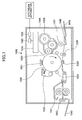
- FIG. 1 is a schematic diagram illustrating a configuration of a laser printer 1000 according to an embodiment of the present invention.
- the laser printer 1000 includes an optical scanning device 1010, a photosensitive drum 1030, a charger 1031, a developing roller 1032, a transfer charger 1033, a discharge unit 1034, a cleaning unit 1035, a toner cartridge 1036, a paper-feed roller 1037, a paper-feed tray 1038, a resist-roller pair 1039, a fusing roller 1041, a paper-eject roller 1042, a paper-catch tray 1043, a communication control unit 1050, and a printer control unit 1060 for controlling other components. These components are placed in the corresponding positions in a printer case 1044.
- the communication control unit 1050 controls two-way communications with an upstream apparatus (e.g., a personal computer) via, for example, a network.
- an upstream apparatus e.g., a personal computer
- the photosensitive drum 1030 is shaped like a cylinder and its surface is covered by a photosensitive layer that is to be scanned by a light beam.
- the photosensitive drum 1030 is configured to rotate in the direction of the arrow shown in FIG. 1 .
- the charger 1031, the developing roller 1032, the transfer charger 1033, the discharge unit 1034, and the cleaning unit 1034 are positioned close to the surface of the photosensitive drum 1030 and are arranged along the rotational direction of the photosensitive drum 1030 in the order mentioned above.
- the charger 1031 uniformly charges the surface of the photosensitive drum 1030.
- the optical scanning device 1010 irradiates the surface of the photosensitive drum 1030 charged by the charger 1031 with a light beam that is modulated according to image information from an upstream apparatus. As a result, a latent image corresponding to the image information is formed on the surface of the photosensitive drum 1030. The formed latent image moves toward the developing roller 1032 as the photosensitive drum 1030 rotates.
- the configuration of the optical scanning device 1010 is described later.
- the toner cartridge 1036 contains toner and supplies the toner to the developing roller 1032.
- the developing roller 1032 causes the toner supplied from the toner cartridge 1036 to adhere to the latent image formed on the photosensitive drum 1030 and thereby develops the latent image.
- the developed latent image (hereafter called a toner image) moves toward the transfer charger 1033 as the photosensitive drum 1030 rotates.
- the paper-feed tray 1038 holds recording paper sheets 1040.
- the paper-feed roller 1037 is positioned close to the paper-feed tray 1038 and feeds the recording paper sheets 1040 one by one from the paper-feed tray 1038 to the resist-roller pair 1039.
- the resist-roller pair 1039 temporarily holds the recording paper sheet 1040 fed from the paper-feed roller 1037 and feeds the paper sheet 1040 into a gap between the photosensitive drum 1030 and the transfer charger 1033 in accordance with the rotation of the photosensitive drum 1030.
- a voltage with a polarity opposite to that of the toner is applied to the transfer charger 1033 to electrically attract the toner on the photosensitive drum 1030 to the recording paper sheet 1040.
- the voltage causes the toner image on the photosensitive drum 1030 to be transferred onto the recording paper sheet 1040.
- the recording paper sheet 1040 with the transferred image is conveyed to the fusing roller 1041.
- the fusing roller 1041 applies heat and pressure to the recording paper sheet 1040 and thereby fuses the toner image onto the recording paper sheet 1040. Then, the recording paper sheet 1040 is ejected by the paper-eject roller 1042 and stacked on the paper-catch tray 1043.
- the discharge unit 1034 discharges the surface of the photosensitive drum 1030.
- the cleaning unit 1035 removes toner (residual toner) remaining on the surface of the photosensitive drum 1030. After the residual toner is removed, the surface of the photosensitive drum 1030 returns to the position facing the charger 1031.
- optical scanning device 1010 An exemplary configuration of the optical scanning device 1010 is described below.
- the optical scanning device 1010 includes a deflector-side scanning lens 11a, an image-surface-side scanning lens 11b, a polygon mirror 13, a light source 14, a coupling lens 15, an aperture plate 16, an anamorphic lens 17, a reflecting mirror 18, and a scan control unit (not shown). These components are placed in corresponding positions in a housing 30.
- a direction corresponding to the main-scanning direction is called a "main-direction" and a direction corresponding to the sub-scanning direction is called a "sub-direction”.
- the coupling lens 15 substantially collimates a light beam emitted from the light source 14.
- the light source 14 and the coupling lens 15 are fixed to a holder made of aluminum and are thereby combined as a unit.
- the aperture plate 16 has an aperture for limiting the diameter of the light beam passing through the coupling lens 15.
- the anamorphic lens 17 causes the,light beam passing through the aperture of the aperture plate 16 to be reflected by the reflecting mirror 18 and focused in the sub-direction near a deflecting surface of the polygon mirror 13.
- the optical system disposed in an optical path between the light source 14 and the polygon mirror 13 is also called a pre-deflector optical system.
- the pre-deflector optical system includes the coupling lens 15, the aperture plate 16, the anamorphic lens 17, and the reflecting mirror 18.
- the polygon mirror 13 for example, is a six-sided mirror with an inradius of 18 mm where each of the six mirrors functions as a deflecting surface.
- the polygon mirror 13 deflects the light beam from the reflecting mirror 18 while rotating at a constant speed about an axis parallel to the sub-direction.
- the deflector-side scanning lens 11a is disposed in a path of the light beam deflected by the polygon mirror 13.
- the image-surface-side scanning lens 11b is disposed in a path of the light beam passing through the deflector-side scanning lens 11a.
- the light beam passing through the image-surface-side scanning lens 11b forms a light spot on the surface of the photosensitive drum 1030.
- the formed light spot moves in the longitudinal direction of the photosensitive drum 1030 as the polygon mirror 13 rotates. In other words, the photosensitive drum 1030 is scanned by the light spot.
- the direction of movement of the light spot is the main-scanning direction, and the direction of rotation of the photosensitive drum 1030 is the sub-scanning direction.
- the optical system disposed in an optical path between the polygon mirror 13 and the photosensitive drum 1030 is also called a scanning optical system.
- the scanning optical system includes the deflector-side scanning lens 11a and the image-surface-side scanning lens 11b.
- one or more bending mirrors may be provided in an optical path between the deflector-side scanning lens 11a and the image-surface-side scanning lens 11b and/or an optical path between the image-surface-side scanning lens 11b and the photosensitive drum 1030.
- the light source 14 includes a surface-emitting laser 100 as exemplified in FIG. 3 .
- the laser oscillation direction is called a Z-axis direction
- two orthogonal directions in a plane perpendicular to the Z-axis direction are called an X-axis direction and a Y-axis direction.
- the surface-emitting laser 100 has a design oscillation wavelength in a 780-nm band and includes a substrate 101, a lower semiconductor DBR 103, a lower spacer layer 104, an active layer 105, an upper spacer layer 106, an upper semiconductor DBR (semiconductor multilayer mirror) 107, and a contact layer 109.
- the lower semiconductor DBR 103 is stacked above the +Z side of the substrate 101 via a buffer layer (not shown) and includes 40.5 pairs of a low-refractive-index layer 103a essentially composed of n-AIAs and a high-refractive-index layer 103b essentially composed of n-Al 0.3 Ga 0.7 As. Between each pair of the refractive-index layers, a composition gradient layer (not shown) having gradually changing composition and a thickness of 20 nm is provided to reduce electric resistance.
- the combined optical thickness of each of the refractive-index layers and one half of the adjoining composition gradient layer is ⁇ /4 where ⁇ indicates the oscillation wavelength.
- the optical thickness of a layer is ⁇ /4
- the actual thickness of the layer is ⁇ /4N where N indicates the refractive index of the medium of the layer.
- the lower spacer layer 104 is stacked on the +Z side of the lower semiconductor DBR 103 and is essentially composed of undoped (Al 0.1 Ga 0.9 ) 0.5 In 0.5 P.
- the active layer 105 is stacked on the +Z side of the lower spacer layer 104 and as exemplified in FIG. 5 , includes three quantum well layers 105a and four barrier layers 105b.
- Each of the quantum well layers 105a is essentially composed of GaInPAs that induces compressive strain of 0.7% and has a band-gap wavelength of about 780 nm.
- Each of the barrier layers 105b is essentially composed of Ga 0.68 In 0.32 P that induces tensile strain of 0.6%.
- the band dispersion of heavy holes and light holes increases. This in turn increases the gain, reduces the threshold, and increases the efficiency (increases the power). This also improves the carrier confinement capability and reduces the threshold, and thereby makes it possible to reduce the reflectance of the upper semiconductor DBR 107, which results in further increase in the power.
- the upper spacer layer 106 is stacked on the +Z side of the active layer 105 and is essentially composed of undoped (Al 0.1 Ga 0.9 ) 0.5 In 0.5 P.
- the lower spacer layer 104, the active layer 105, and the upper spacer layer 106 form a resonator structure having an optical thickness of one wavelength.
- the active layer 105 is positioned in the middle of the resonator structure which corresponds to the peak of electric field standing wave distribution to achieve a high stimulated emission probability.
- the upper semiconductor DBR 107 is stacked on the +Z side of the upper spacer layer 106 and includes 23 pairs of a low-refractive-index layer and a high-refractive-index layer. Between each pair of the refractive-index layers, a composition gradient layer (not shown) having gradually changing composition is provided to reduce electric resistance.
- a selective oxidation layer 108 essentially composed of p-AlAs and having a uniform thickness of 30 nm is inserted in one of the low-refractive-index layers of the upper semiconductor DBR 107.
- the selective oxidation layer 108 is inserted into a third low-refractive-index layer from the upper spacer layer 106 which is at an optical distance of 5 ⁇ /4 from the upper spacer layer 106.
- the combined optical thickness of the low-refractive-index layer including the selective oxidation layer 108 and one half of the adjoining composition gradient layer is 3 ⁇ /4.
- each refractive-index layer of the upper semiconductor DBR 107 other than the low-refractive-index layer including the selective oxidation layer 108 and one half of the adjoining composition gradient layer is ⁇ /4.
- intermediate layers 107m essentially composed of p-Al 0.81 Ga 0.19 As and having a thickness of 38 nm are provided on the -Z and +Z sides of the selective oxidation layer 108.
- the low-refractive layer including the selective oxidation layer 108 further includes layers 107c (hereafter called low-refractive layers 107c) composed essentially of p-Al 0.7 Ga 0.3 As and positioned adjacent to the intermediate layers 107m.
- 107a indicates low-refractive-index layers other than the low-refractive-index layer including the selective oxidation layer 108.
- the low-refractive-index layers 107a are essentially composed of p-Al 0.9 Ga 0.1 As.
- 107b indicates high-refractive-index layers.
- the high-refractive-index layers 107b are essentially composed of pAl 0.3 Ga 0.7 As.
- the contact layer 109 is stacked on the +Z side of the upper semiconductor DBR 107 and is essentially composed of p-GaAs.
- laminated structure a structure made by stacking multiple semiconductor layers on the substrate 101 as described above is called a "laminated structure”.
- the surface-emitting laser 100 produced as described above emitted linearly polarized light and the polarization direction of the light was stable in the X-axis direction as desired.
- the shape (far-field pattern: FFP) of the light beam emitted from the surface-emitting laser 100 was substantially circular.
- FIG. 7 is a cross-sectional view of the surface-emitting laser 100 taken along line A-A of FIG. 3 .
- dy1 indicates the distance between the +Y end of the oxidized layer 108a and the +Y end of the current passage area 108b
- dy2 indicates the distance between the -Y end of the oxidized layer 108a and the -Y end of the current passage area 108b
- dx1 indicates the distance between the +X end of the oxidized layer 108a and the +X end of the current passage area 108b
- dx2 indicates the distance between the -X end of the oxidized layer 108a and the -X end of the current passage area 108b.
- the distances were measured using an IR microscope and the measurement results showed that dy2>dy1 and dx2 ⁇ dx1>dyl.
- dy1 corresponds to the length of oxidation (oxidation length or distance) proceeded in the -Y direction
- dy2 corresponds to the length of oxidation proceeded in the +Y direction
- dx1 corresponds to the length of oxidation proceeded in the -X direction
- dx2 corresponds to the length of oxidation proceeded in the +X direction. Since the oxidation time is constant, the oxidation length increases as the oxidation rate increases. Therefore, the above measurement results indicate that the oxidation rate in the -Y direction is slower than the oxidation rates in the +Y, +X, and -X directions.
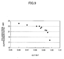
- FIG. 9 shows a relationship between the oxidation rate ratio and the polarization suppression ratio measured in an experiment where only oxidation conditions were changed.
- the polarization suppression ratio is the ratio of the intensity of light in the desired polarization direction to the intensity of light in a direction orthogonal to the desired polarization direction. For example, a polarization suppression ratio of about 20 dB is normally required for a copier.
- the oxidation rate ratio was gradually increased from 0.95.
- the polarization suppression ratio started to decrease when the oxidation rate ratio reached about 0.98, and became smaller than 20 dB when the oxidation rate ratio reached 0.995.
- the polarization suppression ratio of the surface-emitting laser 100 of this embodiment was greater than or equal to 20 dB.
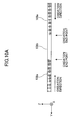
- FIG. 10A is a cross-sectional view of the oxide-confined structure taken along line A-A of FIG. 7 .
- a cross section of the oxidized layer 108a was observed by a transmission electron microscope (TEM). According to the observation result, the cross section of the oxidized layer 108a gently slopes downward in the direction of the oxidation process.
- Sy1 indicates the thickness of the oxidized layer 108a on the +Y side of the current passage area 108b
- Sy2 indicates the thickness of the oxidized layer 108a on the -Y side of the current passage area 108b.
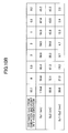
- the thicknesses Sy1 and Sy2 were measured at various positions along the Y-axis. As shown in FIG. 10B , Sy1 was greater than Sy2 at the same distance from the corresponding oxidation end points.
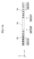
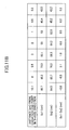
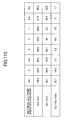
- FIG. 11A is a cross-sectional view of the oxide-confined structure taken along line B-B of FIG. 7 .
- Sx1 indicates the thickness of the oxidized layer 108a on the -X side of the current passage area 108b and Sx2 indicates the thickness of the oxidized layer 108a on the +X side of the current passage area 108b.
- the thicknesses Sx1 and Sx2 were measured at various positions along the X-axis.
- Sx1 and Sx2 were substantially the same at the same distance from the corresponding oxidation end points.
- Sx1 and Sx2 were smaller than Sy1 at the same distance from the corresponding oxidation end points.
- a strain field by the selective oxidation described above can be detected, for example, from a selected-area electron diffraction image obtained by a TEM.
- the strain field caused by the selective oxidation was larger near the oxidation end points and the influence of the strain field on the active layer 105 was observed near the oxidation end points. This means that a local strain has been applied to the active layer 105 by the selective oxidation.
- the inventors of the present invention measured the degree of the local strain (amount of strain) applied to the active layer 105 using a cathodoluminescence (CL) technique.
- CL cathodoluminescence
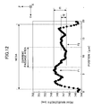
- FIG. 12 is a graph showing measured peak wavelengths of cathodoluminescence in the active layer 105 of the surface-emitting laser 100 at positions along the Y-axis direction.
- variations hereafter called "shift amounts" of the peak wavelengths at positions (F1 and F2) corresponding to the vicinity of the oxidation end points with respect to the peak wavelengths in an area corresponding to the current passage area 108b are positive.
- a shift amount f1 at the position F1 on the +Y side is greater than a shift amount f2 at the position F2 on the -Y side.
- the tensile stress at the position F1 is greater than that at the position F2. It is considered that the difference in tensile stress is caused by the difference between Sy1 and Sy2 (Sy1>Sy2).
- a shift amount of about 1 nm in cathodoluminescence corresponds to an amount of strain of about 0.02% (see, for example, M. Watanabe, H. Matsuura, and N. Shimada; "Investigation of tensile-strained InGaAIP multiquantum-well active regions by photoluminescence measurements”; J. Appl. Phys. 76(12), 15 December, 1994 ).
- the shift amount f1 at the position F1 is about 1 nm greater than the shift amount f2 at the position F2 (see FIG. 12 ). This indicates that a local strain with an anisotropy of about 0.02% has been applied to the active layer 105 of the surface-emitting laser 100.
- FIG. 13 is a graph showing measured peak wavelengths of cathodoluminescence in a degraded surface-emitting laser according to comparative example 1.
- a decrease of the peak wavelength at around 10 ⁇ m is considered to be caused by the decrease in the emission intensity due to degradation and is therefore ignored.
- the shift amounts at positions F3 and F4 corresponding to the vicinity of the oxidation end points were substantially the same and the anisotropy of the local strain applied to the active layer was about 0.002%.
- the polarization state of light of the surface-emitting laser of comparative example 1 was unstable.
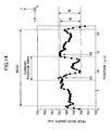
- FIG. 14 is a graph showing measured peak wavelengths of cathodoluminescence in a surface-emitting laser of comparative example 2 having an oxidized layer thicker than that of the surface-emitting laser 100.
- both of the shift amounts at positions F5 and F6 corresponding to the vicinity of the oxidation end points were about 3 nm.
- a shift amount of 3 nm corresponds to an amount of strain of about 0.06%.
- a life test was performed on the surface-emitting laser of comparative example 2 at 60 °C with the output power fixed at 1.4 mW, and the lifetime of the laser was several hundred hours. Compared with a lifetime of several thousand hours of a typical surface-emitting laser, the lifetime of the surface-emitting laser of comparative example 2 is apparently short. With a lifetime of several hundred hours, the surface-emitting laser cannot meet the
Landscapes
- Physics & Mathematics (AREA)
- General Physics & Mathematics (AREA)
- Optics & Photonics (AREA)
- Condensed Matter Physics & Semiconductors (AREA)
- Electromagnetism (AREA)
- Semiconductor Lasers (AREA)
Applications Claiming Priority (2)
| Application Number | Priority Date | Filing Date | Title |
|---|---|---|---|
| JP2008125709 | 2008-05-13 | ||
| JP2009081678A JP5408477B2 (ja) | 2008-05-13 | 2009-03-30 | 面発光レーザ素子、面発光レーザアレイ、光走査装置及び画像形成装置 |
Publications (3)
| Publication Number | Publication Date |
|---|---|
| EP2120303A2 true EP2120303A2 (de) | 2009-11-18 |
| EP2120303A3 EP2120303A3 (de) | 2010-09-29 |
| EP2120303B1 EP2120303B1 (de) | 2014-10-15 |
Family
ID=41011806
Family Applications (1)
| Application Number | Title | Priority Date | Filing Date |
|---|---|---|---|
| EP09251308.4A Not-in-force EP2120303B1 (de) | 2008-05-13 | 2009-05-13 | Oberflächenemittierender Laser, oberflächenemittierendes Laserarray, optische Abtastvorrichtung und Bilderstellungsvorrichtung |
Country Status (6)
| Country | Link |
|---|---|
| US (1) | US8111725B2 (de) |
| EP (1) | EP2120303B1 (de) |
| JP (1) | JP5408477B2 (de) |
| KR (1) | KR101088917B1 (de) |
| CN (2) | CN102324695A (de) |
| TW (1) | TWI405378B (de) |
Families Citing this family (42)
| Publication number | Priority date | Publication date | Assignee | Title |
|---|---|---|---|---|
| JP5515767B2 (ja) | 2009-05-28 | 2014-06-11 | 株式会社リコー | 面発光レーザ素子の製造方法、面発光レーザ素子、面発光レーザアレイ、光走査装置及び画像形成装置 |
| JP5636686B2 (ja) | 2009-06-04 | 2014-12-10 | 株式会社リコー | 面発光レーザアレイ、光走査装置、画像形成装置、及び面発光レーザアレイの製造方法 |
| JP5510899B2 (ja) | 2009-09-18 | 2014-06-04 | 株式会社リコー | 面発光レーザ素子、面発光レーザアレイ、光走査装置、及び画像形成装置 |
| WO2011059833A2 (en) * | 2009-10-29 | 2011-05-19 | California Institute Of Technology | Dual-mode raster point scanning/light sheet illumination microscope |
| JP2011124541A (ja) * | 2009-11-12 | 2011-06-23 | Ricoh Co Ltd | 光デバイス、光走査装置及び画像形成装置、並びに光デバイスの製造方法 |
| JP5532321B2 (ja) * | 2009-11-17 | 2014-06-25 | 株式会社リコー | 面発光レーザ素子、面発光レーザアレイ、光走査装置及び画像形成装置 |
| JP5527714B2 (ja) * | 2009-11-18 | 2014-06-25 | 株式会社リコー | 面発光レーザ素子、面発光レーザアレイ、光走査装置及び画像形成装置 |
| JP5522595B2 (ja) * | 2009-11-27 | 2014-06-18 | 株式会社リコー | 面発光レーザ素子、面発光レーザアレイ、光走査装置及び画像形成装置 |
| JP2011151357A (ja) | 2009-12-21 | 2011-08-04 | Ricoh Co Ltd | 光デバイス、光走査装置及び画像形成装置 |
| JP2011159943A (ja) | 2010-01-08 | 2011-08-18 | Ricoh Co Ltd | 面発光レーザ素子、面発光レーザアレイ、光走査装置及び画像形成装置 |
| JP2011166108A (ja) * | 2010-01-15 | 2011-08-25 | Ricoh Co Ltd | 面発光レーザ素子、面発光レーザアレイ、光走査装置及び画像形成装置 |
| JP5834414B2 (ja) * | 2010-03-18 | 2015-12-24 | 株式会社リコー | 面発光レーザモジュール、光走査装置及び画像形成装置 |
| JP5585940B2 (ja) | 2010-04-22 | 2014-09-10 | 株式会社リコー | 面発光レーザ素子、面発光レーザアレイ、光走査装置、画像形成装置及び面発光レーザ素子の製造方法 |
| JP5601014B2 (ja) | 2010-04-23 | 2014-10-08 | 株式会社リコー | 光デバイス、光走査装置及び画像形成装置 |
| JP2011249763A (ja) | 2010-04-28 | 2011-12-08 | Ricoh Co Ltd | 光源ユニット、光走査装置及び画像形成装置 |
| JP5754624B2 (ja) | 2010-05-25 | 2015-07-29 | 株式会社リコー | 面発光レーザ素子、面発光レーザアレイ、光走査装置、画像形成装置及び面発光レーザ素子の製造方法 |
| JP5721055B2 (ja) | 2010-06-11 | 2015-05-20 | 株式会社リコー | 面発光レーザ素子、面発光レーザアレイ、光走査装置、画像形成装置及び面発光レーザ素子の製造方法 |
| CN102447220A (zh) * | 2010-09-30 | 2012-05-09 | 新科实业有限公司 | 面发光型半导体激光器及其制造方法 |
| JP5725804B2 (ja) * | 2010-11-05 | 2015-05-27 | キヤノン株式会社 | 面発光レーザ及び面発光レーザアレイ、面発光レーザの製造方法及び面発光レーザアレイの製造方法、面発光レーザアレイを備えた光学機器 |
| US9267886B2 (en) | 2010-11-26 | 2016-02-23 | Ricoh Company, Ltd. | Optical sensor and image forming apparatus |
| JP2012209534A (ja) | 2011-03-17 | 2012-10-25 | Ricoh Co Ltd | 面発光レーザ素子、原子発振器及び面発光レーザ素子の検査方法 |
| JP5929259B2 (ja) | 2011-05-17 | 2016-06-01 | 株式会社リコー | 面発光レーザ素子、光走査装置及び画像形成装置 |
| JP5999303B2 (ja) * | 2011-06-24 | 2016-09-28 | 株式会社リコー | 面発光レーザアレイ及び画像形成装置 |
| JP2013051398A (ja) | 2011-08-01 | 2013-03-14 | Ricoh Co Ltd | 面発光レーザ素子、光走査装置及び画像形成装置 |
| JP6021307B2 (ja) * | 2011-09-06 | 2016-11-09 | キヤノン株式会社 | 半導体レーザの劣化兆候検出装置及び半導体レーザの劣化兆候検出方法 |
| JP6303255B2 (ja) | 2011-12-02 | 2018-04-04 | 株式会社リコー | 面発光レーザ素子及び原子発振器 |
| JP2013131509A (ja) | 2011-12-20 | 2013-07-04 | Ricoh Co Ltd | 光学ユニットの製造方法、光学ユニット、光走査装置及び画像形成装置 |
| JP5999304B2 (ja) | 2012-02-17 | 2016-09-28 | 株式会社リコー | 光学センサ及び画像形成装置 |
| JP5999305B2 (ja) | 2012-02-20 | 2016-09-28 | 株式会社リコー | 光学センサ及び画像形成装置 |
| JP5939461B2 (ja) | 2012-03-01 | 2016-06-22 | 株式会社リコー | 光学センサ及び画像形成装置 |
| JP6107089B2 (ja) | 2012-11-30 | 2017-04-05 | 株式会社リコー | 面発光レーザ素子及び原子発振器 |
| JP6299955B2 (ja) * | 2013-12-20 | 2018-03-28 | セイコーエプソン株式会社 | 面発光レーザーおよび原子発振器 |
| JP2015119140A (ja) * | 2013-12-20 | 2015-06-25 | セイコーエプソン株式会社 | 面発光レーザーおよび原子発振器 |
| US9966730B2 (en) | 2014-08-11 | 2018-05-08 | Ricoh Company, Ltd. | Surface-emitting laser apparatus and manufacturing method thereof |
| JP2016174136A (ja) | 2015-03-16 | 2016-09-29 | 株式会社リコー | 面発光レーザアレイ、レーザ装置、点火装置、及び内燃機関 |
| WO2017094778A1 (ja) | 2015-12-02 | 2017-06-08 | 株式会社リコー | レーザ装置、点火装置及び内燃機関 |
| JP6662013B2 (ja) | 2015-12-11 | 2020-03-11 | 株式会社リコー | 面発光レーザ、面発光レーザアレイ、レーザ装置、点火装置、内燃機関、光走査装置、画像形成装置、光伝送モジュール、及び光伝送システム |
| US10516251B2 (en) * | 2016-06-28 | 2019-12-24 | Vi Systems Gmbh | Reliable high-speed oxide-confined vertical-cavity surface-emitting laser |
| US11283240B2 (en) * | 2018-01-09 | 2022-03-22 | Oepic Semiconductors, Inc. | Pillar confined backside emitting VCSEL |
| US11233377B2 (en) * | 2018-01-26 | 2022-01-25 | Oepic Semiconductors Inc. | Planarization of backside emitting VCSEL and method of manufacturing the same for array application |
| JP7434849B2 (ja) | 2019-11-29 | 2024-02-21 | 株式会社リコー | 面発光レーザ、面発光レーザ装置、光源装置及び検出装置 |
| CN110957635B (zh) * | 2020-02-25 | 2020-09-01 | 常州纵慧芯光半导体科技有限公司 | 一种实现偏振控制的vcsel器件及其制备方法 |
Citations (7)
| Publication number | Priority date | Publication date | Assignee | Title |
|---|---|---|---|---|
| JPH0410095B2 (de) | 1982-05-14 | 1992-02-24 | ||
| JP2891133B2 (ja) | 1994-10-24 | 1999-05-17 | 日本電気株式会社 | 面発光レーザ及び面発光レーザアレイ及び光情報処理装置 |
| JP3551718B2 (ja) | 1997-08-18 | 2004-08-11 | 富士ゼロックス株式会社 | 面発光型半導体レーザ |
| JP3606059B2 (ja) | 1998-03-11 | 2005-01-05 | セイコーエプソン株式会社 | 面発光型半導体レーザ及びその製造方法 |
| JP2006013366A (ja) | 2004-06-29 | 2006-01-12 | Fuji Xerox Co Ltd | 面発光型半導体レーザ装置およびその製造方法 |
| JP3799667B2 (ja) | 1996-07-10 | 2006-07-19 | 富士ゼロックス株式会社 | 面発光型半導体レーザ装置およびその製造方法 |
| JP3800852B2 (ja) | 1999-03-10 | 2006-07-26 | 富士ゼロックス株式会社 | 面発光型半導体レーザ及びその製造方法 |
Family Cites Families (42)
| Publication number | Priority date | Publication date | Assignee | Title |
|---|---|---|---|---|
| US6233264B1 (en) * | 1996-08-27 | 2001-05-15 | Ricoh Company, Ltd. | Optical semiconductor device having an active layer containing N |
| JP3449516B2 (ja) * | 1996-08-30 | 2003-09-22 | 株式会社リコー | 半導体多層膜反射鏡および半導体多層膜反射防止膜および面発光型半導体レーザおよび受光素子 |
| JP3467153B2 (ja) * | 1996-08-30 | 2003-11-17 | 株式会社リコー | 半導体素子 |
| JP3788831B2 (ja) * | 1996-08-30 | 2006-06-21 | 株式会社リコー | 半導体素子およびその製造方法 |
| US6072196A (en) * | 1996-09-05 | 2000-06-06 | Ricoh Company, Ltd. | semiconductor light emitting devices |
| US6563851B1 (en) * | 1998-04-13 | 2003-05-13 | Ricoh Company, Ltd. | Laser diode having an active layer containing N and operable in a 0.6 μm wavelength band |
| US6207973B1 (en) * | 1998-08-19 | 2001-03-27 | Ricoh Company, Ltd. | Light emitting devices with layered III-V semiconductor structures |
| US6542528B1 (en) * | 1999-02-15 | 2003-04-01 | Ricoh Company, Ltd. | Light-emitting semiconductor device producing red wavelength optical radiation |
| US6614821B1 (en) * | 1999-08-04 | 2003-09-02 | Ricoh Company, Ltd. | Laser diode and semiconductor light-emitting device producing visible-wavelength radiation |
| JP4010095B2 (ja) * | 1999-10-01 | 2007-11-21 | 富士ゼロックス株式会社 | 面発光型半導体レーザ及びレーザアレイ |
| US6975663B2 (en) * | 2001-02-26 | 2005-12-13 | Ricoh Company, Ltd. | Surface-emission laser diode operable in the wavelength band of 1.1-7μm and optical telecommunication system using such a laser diode |
| US6674777B1 (en) * | 2000-08-31 | 2004-01-06 | Honeywell International Inc. | Protective side wall passivation for VCSEL chips |
| US6674785B2 (en) * | 2000-09-21 | 2004-01-06 | Ricoh Company, Ltd. | Vertical-cavity, surface-emission type laser diode and fabrication process thereof |
| US6570905B1 (en) * | 2000-11-02 | 2003-05-27 | U-L-M Photonics Gmbh | Vertical cavity surface emitting laser with reduced parasitic capacitance |
| US6803604B2 (en) * | 2001-03-13 | 2004-10-12 | Ricoh Company, Ltd. | Semiconductor optical modulator, an optical amplifier and an integrated semiconductor light-emitting device |
| US6765232B2 (en) * | 2001-03-27 | 2004-07-20 | Ricoh Company, Ltd. | Semiconductor light-emitting device, surface-emission laser diode, and production apparatus thereof, production method, optical module and optical telecommunication system |
| JP4537658B2 (ja) * | 2002-02-22 | 2010-09-01 | 株式会社リコー | 面発光レーザ素子、該面発光レーザ素子を用いた面発光レーザアレイ、電子写真システム、面発光レーザモジュール、光通信システム、光インターコネクションシステム、および面発光レーザ素子の製造方法 |
| JP4334845B2 (ja) | 2002-10-15 | 2009-09-30 | 株式会社リコー | 面発光レーザ及び面発光レーザアレイ及び光送信モジュール及び光送受信モジュール及び光通信システム及びレーザプリンター及び光ピックアップシステム |
| US6927412B2 (en) * | 2002-11-21 | 2005-08-09 | Ricoh Company, Ltd. | Semiconductor light emitter |
| US7374976B2 (en) * | 2002-11-22 | 2008-05-20 | Semiconductor Energy Laboratory Co., Ltd. | Method for fabricating thin film transistor |
| JP4184769B2 (ja) * | 2002-11-26 | 2008-11-19 | 株式会社東芝 | 面発光型半導体レーザ及びその製造方法 |
| US7227196B2 (en) * | 2003-05-20 | 2007-06-05 | Burgener Ii Robert H | Group II-VI semiconductor devices |
| US7141489B2 (en) * | 2003-05-20 | 2006-11-28 | Burgener Ii Robert H | Fabrication of p-type group II-VI semiconductors |
| JP4138629B2 (ja) * | 2003-11-06 | 2008-08-27 | 株式会社東芝 | 面発光型半導体素子及びその製造方法 |
| JP2005142479A (ja) | 2003-11-10 | 2005-06-02 | Sony Corp | 半導体発光素子 |
| US7542499B2 (en) * | 2003-11-27 | 2009-06-02 | Ricoh Company, Ltd. | Surface-emission laser diode and surface-emission laser array, optical interconnection system, optical communication system, electrophotographic system, and optical disk system |
| JP5057354B2 (ja) | 2004-04-30 | 2012-10-24 | 株式会社リコー | 面発光レーザの製造方法 |
| EP1780849B1 (de) * | 2004-06-11 | 2013-01-30 | Ricoh Company, Ltd. | Oberflächenemissions-laserdiode und herstellungsverfahren dafür |
| JP4919639B2 (ja) * | 2004-10-13 | 2012-04-18 | 株式会社リコー | 面発光レーザ素子および面発光レーザアレイおよび面発光レーザ素子の製造方法および面発光レーザモジュールおよび電子写真システムおよび光通信システムおよび光インターコネクションシステム |
| JP4568125B2 (ja) * | 2005-01-17 | 2010-10-27 | 株式会社東芝 | 面発光型半導体素子 |
| JP4485972B2 (ja) * | 2005-02-15 | 2010-06-23 | 株式会社リコー | 半導体酸化装置及び半導体素子の製造方法 |
| JP5194432B2 (ja) * | 2005-11-30 | 2013-05-08 | 株式会社リコー | 面発光レーザ素子 |
| US7693204B2 (en) * | 2006-02-03 | 2010-04-06 | Ricoh Company, Ltd. | Surface-emitting laser device and surface-emitting laser array including same |
| WO2007089042A1 (en) | 2006-02-03 | 2007-08-09 | Ricoh Company, Ltd. | Surface-emitting laser device and surface-emitting laser array including same |
| JP5005937B2 (ja) * | 2006-03-24 | 2012-08-22 | 古河電気工業株式会社 | 面発光レーザ素子 |
| JP5224159B2 (ja) | 2006-04-28 | 2013-07-03 | 株式会社リコー | 面発光レーザアレイ、光走査装置及び画像形成装置 |
| TW200743911A (en) * | 2006-05-22 | 2007-12-01 | Chunghwa Telecom Co Ltd | Method of manufacturing vertical-cavity surface-emitting laser mode selection by using self-aligned technique |
| US7800805B2 (en) * | 2006-07-24 | 2010-09-21 | Ricoh Company, Limited | Optical Scanning apparatus and image forming apparatus |
| JP5309485B2 (ja) * | 2006-08-30 | 2013-10-09 | 株式会社リコー | 面発光レーザ、面発光レーザアレイ、光走査装置及び画像形成装置 |
| JP2008060322A (ja) * | 2006-08-31 | 2008-03-13 | Ricoh Co Ltd | 面発光レーザ素子、面発光レーザアレイ、光走査装置、画像形成装置及び光通信システム |
| JP2008064801A (ja) * | 2006-09-04 | 2008-03-21 | Ricoh Co Ltd | 光走査装置及び画像形成装置 |
| US20090278233A1 (en) * | 2007-07-26 | 2009-11-12 | Pinnington Thomas Henry | Bonded intermediate substrate and method of making same |
-
2009
- 2009-03-30 JP JP2009081678A patent/JP5408477B2/ja active Active
- 2009-05-12 KR KR1020090041358A patent/KR101088917B1/ko not_active Expired - Fee Related
- 2009-05-12 US US12/464,408 patent/US8111725B2/en active Active
- 2009-05-13 TW TW098115879A patent/TWI405378B/zh active
- 2009-05-13 EP EP09251308.4A patent/EP2120303B1/de not_active Not-in-force
- 2009-05-13 CN CN2011102733003A patent/CN102324695A/zh active Pending
- 2009-05-13 CN CN2009101393878A patent/CN101582563B/zh active Active
Patent Citations (7)
| Publication number | Priority date | Publication date | Assignee | Title |
|---|---|---|---|---|
| JPH0410095B2 (de) | 1982-05-14 | 1992-02-24 | ||
| JP2891133B2 (ja) | 1994-10-24 | 1999-05-17 | 日本電気株式会社 | 面発光レーザ及び面発光レーザアレイ及び光情報処理装置 |
| JP3799667B2 (ja) | 1996-07-10 | 2006-07-19 | 富士ゼロックス株式会社 | 面発光型半導体レーザ装置およびその製造方法 |
| JP3551718B2 (ja) | 1997-08-18 | 2004-08-11 | 富士ゼロックス株式会社 | 面発光型半導体レーザ |
| JP3606059B2 (ja) | 1998-03-11 | 2005-01-05 | セイコーエプソン株式会社 | 面発光型半導体レーザ及びその製造方法 |
| JP3800852B2 (ja) | 1999-03-10 | 2006-07-26 | 富士ゼロックス株式会社 | 面発光型半導体レーザ及びその製造方法 |
| JP2006013366A (ja) | 2004-06-29 | 2006-01-12 | Fuji Xerox Co Ltd | 面発光型半導体レーザ装置およびその製造方法 |
Non-Patent Citations (2)
| Title |
|---|
| M. WATANABE; H. MATSUURA; N. SHIMADA: "Investigation of tensile-strained InGaAIP multiquantum-well active regions by photoluminescence measurements", J. APPL. PHYS., vol. 76, no. 12, 15 December 1994 (1994-12-15) |
| T. OHTOSH ET AL.: "Dependence of optical gain on crystal orientation in surface-emitting lasers with strained quantum wells", APPL. PHYS. LETT., vol. 65, no. 15, 10 October 1994 (1994-10-10) |
Also Published As
| Publication number | Publication date |
|---|---|
| EP2120303A3 (de) | 2010-09-29 |
| KR20090118862A (ko) | 2009-11-18 |
| JP5408477B2 (ja) | 2014-02-05 |
| EP2120303B1 (de) | 2014-10-15 |
| TWI405378B (zh) | 2013-08-11 |
| CN102324695A (zh) | 2012-01-18 |
| US20090285252A1 (en) | 2009-11-19 |
| CN101582563B (zh) | 2011-11-16 |
| TW201008065A (en) | 2010-02-16 |
| JP2009302513A (ja) | 2009-12-24 |
| US8111725B2 (en) | 2012-02-07 |
| KR101088917B1 (ko) | 2011-12-01 |
| CN101582563A (zh) | 2009-11-18 |
Similar Documents
| Publication | Publication Date | Title |
|---|---|---|
| EP2120303B1 (de) | Oberflächenemittierender Laser, oberflächenemittierendes Laserarray, optische Abtastvorrichtung und Bilderstellungsvorrichtung | |
| KR101357925B1 (ko) | 면 발광 레이저, 면 발광 레이저 어레이, 광 주사 장치, 및 화상 형성 장치 | |
| JP5316783B2 (ja) | 面発光レーザ素子、面発光レーザアレイ、光走査装置及び画像形成装置 | |
| US8208511B2 (en) | Surface emitting laser, surface emitting laser array, optical scanning device, image forming apparatus, optical transmission module and optical transmission system | |
| KR101292390B1 (ko) | 수직 공진기형 면발광 레이저 소자, 수직 공진기형 면발광 레이저 어레이, 광 주사 장치 및 화상 형성 장치 | |
| JP5316784B2 (ja) | 面発光レーザ素子、面発光レーザアレイ、光走査装置及び画像形成装置 | |
| JP5261754B2 (ja) | 面発光レーザ素子、面発光レーザアレイ、光走査装置及び画像形成装置 | |
| JP2011135030A (ja) | 面発光レーザ素子、面発光レーザアレイ、光走査装置及び画像形成装置 | |
| US8275014B2 (en) | Surface-emitting laser element, surface-emitting laser array, optical scanning device, and image forming apparatus | |
| JP6015982B2 (ja) | 面発光レーザ、光走査装置及び画像形成装置 | |
| JP5505614B2 (ja) | 面発光レーザ素子、面発光レーザアレイ、光走査装置及び画像形成装置 | |
| JP2016106433A (ja) | 面発光レーザ素子、面発光レーザアレイ、光走査装置及び画像形成装置 | |
| JP2015053496A (ja) | 面発光レーザ素子、面発光レーザアレイ、光走査装置及び画像形成装置 | |
| JP2014168082A (ja) | 面発光レーザ素子、面発光レーザアレイ、光走査装置及び画像形成装置 |
Legal Events
| Date | Code | Title | Description |
|---|---|---|---|
| PUAI | Public reference made under article 153(3) epc to a published international application that has entered the european phase |
Free format text: ORIGINAL CODE: 0009012 |
|
| 17P | Request for examination filed |
Effective date: 20090529 |
|
| AK | Designated contracting states |
Kind code of ref document: A2 Designated state(s): AT BE BG CH CY CZ DE DK EE ES FI FR GB GR HR HU IE IS IT LI LT LU LV MC MK MT NL NO PL PT RO SE SI SK TR |
|
| PUAL | Search report despatched |
Free format text: ORIGINAL CODE: 0009013 |
|
| RIC1 | Information provided on ipc code assigned before grant |
Ipc: G03G 15/00 20060101ALI20100728BHEP Ipc: H01S 5/18 20060101AFI20090907BHEP Ipc: H01S 5/42 20060101ALI20100728BHEP |
|
| AK | Designated contracting states |
Kind code of ref document: A3 Designated state(s): AT BE BG CH CY CZ DE DK EE ES FI FR GB GR HR HU IE IS IT LI LT LU LV MC MK MT NL NO PL PT RO SE SI SK TR |
|
| AX | Request for extension of the european patent |
Extension state: AL BA RS |
|
| 17Q | First examination report despatched |
Effective date: 20111028 |
|
| RIC1 | Information provided on ipc code assigned before grant |
Ipc: G03G 15/04 20060101ALI20140403BHEP Ipc: H01S 5/18 20060101AFI20140403BHEP Ipc: H01S 5/42 20060101ALI20140403BHEP Ipc: G03G 15/00 20060101ALI20140403BHEP Ipc: H01S 5/183 20060101ALI20140403BHEP Ipc: H01S 5/32 20060101ALI20140403BHEP |
|
| GRAP | Despatch of communication of intention to grant a patent |
Free format text: ORIGINAL CODE: EPIDOSNIGR1 |
|
| INTG | Intention to grant announced |
Effective date: 20140521 |
|
| RIN1 | Information on inventor provided before grant (corrected) |
Inventor name: ISHII, TOSHIHIRO Inventor name: JIKUTANI, NAOTO Inventor name: SUGAWARA, SATORU Inventor name: MAKITA, KENGO Inventor name: SATO, SHUNICHI Inventor name: HARASAKA, KAZUHIRO |
|
| RIN1 | Information on inventor provided before grant (corrected) |
Inventor name: SUGAWARA, SATORU Inventor name: HARASAKA, KAZUHIRO Inventor name: MAKITA, KENGO Inventor name: SATO, SHUNICHI Inventor name: JIKUTANI, NAOTO Inventor name: ISHII, TOSHIHIRO |
|
| GRAS | Grant fee paid |
Free format text: ORIGINAL CODE: EPIDOSNIGR3 |
|
| GRAA | (expected) grant |
Free format text: ORIGINAL CODE: 0009210 |
|
| AK | Designated contracting states |
Kind code of ref document: B1 Designated state(s): AT BE BG CH CY CZ DE DK EE ES FI FR GB GR HR HU IE IS IT LI LT LU LV MC MK MT NL NO PL PT RO SE SI SK TR |
|
| REG | Reference to a national code |
Ref country code: GB Ref legal event code: FG4D Ref country code: CH Ref legal event code: EP |
|
| REG | Reference to a national code |
Ref country code: IE Ref legal event code: FG4D |
|
| REG | Reference to a national code |
Ref country code: AT Ref legal event code: REF Ref document number: 692024 Country of ref document: AT Kind code of ref document: T Effective date: 20141115 |
|
| REG | Reference to a national code |
Ref country code: DE Ref legal event code: R096 Ref document number: 602009027177 Country of ref document: DE Effective date: 20141127 |
|
| REG | Reference to a national code |
Ref country code: NL Ref legal event code: VDEP Effective date: 20141015 |
|
| REG | Reference to a national code |
Ref country code: AT Ref legal event code: MK05 Ref document number: 692024 Country of ref document: AT Kind code of ref document: T Effective date: 20141015 |
|
| REG | Reference to a national code |
Ref country code: LT Ref legal event code: MG4D |
|
| PG25 | Lapsed in a contracting state [announced via postgrant information from national office to epo] |
Ref country code: NL Free format text: LAPSE BECAUSE OF FAILURE TO SUBMIT A TRANSLATION OF THE DESCRIPTION OR TO PAY THE FEE WITHIN THE PRESCRIBED TIME-LIMIT Effective date: 20141015 |
|
| PG25 | Lapsed in a contracting state [announced via postgrant information from national office to epo] |
Ref country code: FI Free format text: LAPSE BECAUSE OF FAILURE TO SUBMIT A TRANSLATION OF THE DESCRIPTION OR TO PAY THE FEE WITHIN THE PRESCRIBED TIME-LIMIT Effective date: 20141015 Ref country code: LT Free format text: LAPSE BECAUSE OF FAILURE TO SUBMIT A TRANSLATION OF THE DESCRIPTION OR TO PAY THE FEE WITHIN THE PRESCRIBED TIME-LIMIT Effective date: 20141015 Ref country code: IS Free format text: LAPSE BECAUSE OF FAILURE TO SUBMIT A TRANSLATION OF THE DESCRIPTION OR TO PAY THE FEE WITHIN THE PRESCRIBED TIME-LIMIT Effective date: 20150215 Ref country code: NO Free format text: LAPSE BECAUSE OF FAILURE TO SUBMIT A TRANSLATION OF THE DESCRIPTION OR TO PAY THE FEE WITHIN THE PRESCRIBED TIME-LIMIT Effective date: 20150115 Ref country code: PT Free format text: LAPSE BECAUSE OF FAILURE TO SUBMIT A TRANSLATION OF THE DESCRIPTION OR TO PAY THE FEE WITHIN THE PRESCRIBED TIME-LIMIT Effective date: 20150216 Ref country code: ES Free format text: LAPSE BECAUSE OF FAILURE TO SUBMIT A TRANSLATION OF THE DESCRIPTION OR TO PAY THE FEE WITHIN THE PRESCRIBED TIME-LIMIT Effective date: 20141015 |
|
| PG25 | Lapsed in a contracting state [announced via postgrant information from national office to epo] |
Ref country code: SE Free format text: LAPSE BECAUSE OF FAILURE TO SUBMIT A TRANSLATION OF THE DESCRIPTION OR TO PAY THE FEE WITHIN THE PRESCRIBED TIME-LIMIT Effective date: 20141015 Ref country code: PL Free format text: LAPSE BECAUSE OF FAILURE TO SUBMIT A TRANSLATION OF THE DESCRIPTION OR TO PAY THE FEE WITHIN THE PRESCRIBED TIME-LIMIT Effective date: 20141015 Ref country code: AT Free format text: LAPSE BECAUSE OF FAILURE TO SUBMIT A TRANSLATION OF THE DESCRIPTION OR TO PAY THE FEE WITHIN THE PRESCRIBED TIME-LIMIT Effective date: 20141015 Ref country code: LV Free format text: LAPSE BECAUSE OF FAILURE TO SUBMIT A TRANSLATION OF THE DESCRIPTION OR TO PAY THE FEE WITHIN THE PRESCRIBED TIME-LIMIT Effective date: 20141015 Ref country code: GR Free format text: LAPSE BECAUSE OF FAILURE TO SUBMIT A TRANSLATION OF THE DESCRIPTION OR TO PAY THE FEE WITHIN THE PRESCRIBED TIME-LIMIT Effective date: 20150116 Ref country code: CY Free format text: LAPSE BECAUSE OF FAILURE TO SUBMIT A TRANSLATION OF THE DESCRIPTION OR TO PAY THE FEE WITHIN THE PRESCRIBED TIME-LIMIT Effective date: 20141015 Ref country code: HR Free format text: LAPSE BECAUSE OF FAILURE TO SUBMIT A TRANSLATION OF THE DESCRIPTION OR TO PAY THE FEE WITHIN THE PRESCRIBED TIME-LIMIT Effective date: 20141015 |
|
| REG | Reference to a national code |
Ref country code: DE Ref legal event code: R097 Ref document number: 602009027177 Country of ref document: DE |
|
| PG25 | Lapsed in a contracting state [announced via postgrant information from national office to epo] |
Ref country code: DK Free format text: LAPSE BECAUSE OF FAILURE TO SUBMIT A TRANSLATION OF THE DESCRIPTION OR TO PAY THE FEE WITHIN THE PRESCRIBED TIME-LIMIT Effective date: 20141015 Ref country code: CZ Free format text: LAPSE BECAUSE OF FAILURE TO SUBMIT A TRANSLATION OF THE DESCRIPTION OR TO PAY THE FEE WITHIN THE PRESCRIBED TIME-LIMIT Effective date: 20141015 Ref country code: EE Free format text: LAPSE BECAUSE OF FAILURE TO SUBMIT A TRANSLATION OF THE DESCRIPTION OR TO PAY THE FEE WITHIN THE PRESCRIBED TIME-LIMIT Effective date: 20141015 Ref country code: RO Free format text: LAPSE BECAUSE OF FAILURE TO SUBMIT A TRANSLATION OF THE DESCRIPTION OR TO PAY THE FEE WITHIN THE PRESCRIBED TIME-LIMIT Effective date: 20141015 Ref country code: SK Free format text: LAPSE BECAUSE OF FAILURE TO SUBMIT A TRANSLATION OF THE DESCRIPTION OR TO PAY THE FEE WITHIN THE PRESCRIBED TIME-LIMIT Effective date: 20141015 |
|
| PLBE | No opposition filed within time limit |
Free format text: ORIGINAL CODE: 0009261 |
|
| STAA | Information on the status of an ep patent application or granted ep patent |
Free format text: STATUS: NO OPPOSITION FILED WITHIN TIME LIMIT |
|
| PG25 | Lapsed in a contracting state [announced via postgrant information from national office to epo] |
Ref country code: IT Free format text: LAPSE BECAUSE OF FAILURE TO SUBMIT A TRANSLATION OF THE DESCRIPTION OR TO PAY THE FEE WITHIN THE PRESCRIBED TIME-LIMIT Effective date: 20141015 |
|
| 26N | No opposition filed |
Effective date: 20150716 |
|
| REG | Reference to a national code |
Ref country code: CH Ref legal event code: PL |
|
| PG25 | Lapsed in a contracting state [announced via postgrant information from national office to epo] |
Ref country code: CH Free format text: LAPSE BECAUSE OF NON-PAYMENT OF DUE FEES Effective date: 20150531 Ref country code: LI Free format text: LAPSE BECAUSE OF NON-PAYMENT OF DUE FEES Effective date: 20150531 Ref country code: MC Free format text: LAPSE BECAUSE OF FAILURE TO SUBMIT A TRANSLATION OF THE DESCRIPTION OR TO PAY THE FEE WITHIN THE PRESCRIBED TIME-LIMIT Effective date: 20141015 Ref country code: LU Free format text: LAPSE BECAUSE OF FAILURE TO SUBMIT A TRANSLATION OF THE DESCRIPTION OR TO PAY THE FEE WITHIN THE PRESCRIBED TIME-LIMIT Effective date: 20150513 |
|
| REG | Reference to a national code |
Ref country code: IE Ref legal event code: MM4A |
|
| PG25 | Lapsed in a contracting state [announced via postgrant information from national office to epo] |
Ref country code: SI Free format text: LAPSE BECAUSE OF FAILURE TO SUBMIT A TRANSLATION OF THE DESCRIPTION OR TO PAY THE FEE WITHIN THE PRESCRIBED TIME-LIMIT Effective date: 20141015 |
|
| PG25 | Lapsed in a contracting state [announced via postgrant information from national office to epo] |
Ref country code: IE Free format text: LAPSE BECAUSE OF NON-PAYMENT OF DUE FEES Effective date: 20150513 |
|
| REG | Reference to a national code |
Ref country code: FR Ref legal event code: PLFP Year of fee payment: 8 |
|
| PG25 | Lapsed in a contracting state [announced via postgrant information from national office to epo] |
Ref country code: MT Free format text: LAPSE BECAUSE OF FAILURE TO SUBMIT A TRANSLATION OF THE DESCRIPTION OR TO PAY THE FEE WITHIN THE PRESCRIBED TIME-LIMIT Effective date: 20141015 |
|
| REG | Reference to a national code |
Ref country code: FR Ref legal event code: PLFP Year of fee payment: 9 |
|
| PG25 | Lapsed in a contracting state [announced via postgrant information from national office to epo] |
Ref country code: BG Free format text: LAPSE BECAUSE OF FAILURE TO SUBMIT A TRANSLATION OF THE DESCRIPTION OR TO PAY THE FEE WITHIN THE PRESCRIBED TIME-LIMIT Effective date: 20141015 Ref country code: HU Free format text: LAPSE BECAUSE OF FAILURE TO SUBMIT A TRANSLATION OF THE DESCRIPTION OR TO PAY THE FEE WITHIN THE PRESCRIBED TIME-LIMIT; INVALID AB INITIO Effective date: 20090513 |
|
| PG25 | Lapsed in a contracting state [announced via postgrant information from national office to epo] |
Ref country code: TR Free format text: LAPSE BECAUSE OF FAILURE TO SUBMIT A TRANSLATION OF THE DESCRIPTION OR TO PAY THE FEE WITHIN THE PRESCRIBED TIME-LIMIT Effective date: 20141015 |
|
| PG25 | Lapsed in a contracting state [announced via postgrant information from national office to epo] |
Ref country code: BE Free format text: LAPSE BECAUSE OF FAILURE TO SUBMIT A TRANSLATION OF THE DESCRIPTION OR TO PAY THE FEE WITHIN THE PRESCRIBED TIME-LIMIT Effective date: 20141015 |
|
| REG | Reference to a national code |
Ref country code: FR Ref legal event code: PLFP Year of fee payment: 10 |
|
| PG25 | Lapsed in a contracting state [announced via postgrant information from national office to epo] |
Ref country code: MK Free format text: LAPSE BECAUSE OF FAILURE TO SUBMIT A TRANSLATION OF THE DESCRIPTION OR TO PAY THE FEE WITHIN THE PRESCRIBED TIME-LIMIT Effective date: 20141015 |
|
| PGFP | Annual fee paid to national office [announced via postgrant information from national office to epo] |
Ref country code: FR Payment date: 20210525 Year of fee payment: 13 Ref country code: DE Payment date: 20210520 Year of fee payment: 13 |
|
| PGFP | Annual fee paid to national office [announced via postgrant information from national office to epo] |
Ref country code: GB Payment date: 20210520 Year of fee payment: 13 |
|
| REG | Reference to a national code |
Ref country code: DE Ref legal event code: R119 Ref document number: 602009027177 Country of ref document: DE |
|
| GBPC | Gb: european patent ceased through non-payment of renewal fee |
Effective date: 20220513 |
|
| PG25 | Lapsed in a contracting state [announced via postgrant information from national office to epo] |
Ref country code: FR Free format text: LAPSE BECAUSE OF NON-PAYMENT OF DUE FEES Effective date: 20220531 |
|
| PG25 | Lapsed in a contracting state [announced via postgrant information from national office to epo] |
Ref country code: GB Free format text: LAPSE BECAUSE OF NON-PAYMENT OF DUE FEES Effective date: 20220513 Ref country code: DE Free format text: LAPSE BECAUSE OF NON-PAYMENT OF DUE FEES Effective date: 20221201 |