EP2120342A1 - Digitaler Phasenregelkreis - Google Patents
Digitaler Phasenregelkreis Download PDFInfo
- Publication number
- EP2120342A1 EP2120342A1 EP09160318A EP09160318A EP2120342A1 EP 2120342 A1 EP2120342 A1 EP 2120342A1 EP 09160318 A EP09160318 A EP 09160318A EP 09160318 A EP09160318 A EP 09160318A EP 2120342 A1 EP2120342 A1 EP 2120342A1
- Authority
- EP
- European Patent Office
- Prior art keywords
- phase
- signal
- input signal
- vco
- locked loop
- Prior art date
- Legal status (The legal status is an assumption and is not a legal conclusion. Google has not performed a legal analysis and makes no representation as to the accuracy of the status listed.)
- Withdrawn
Links
- 238000000605 extraction Methods 0.000 claims abstract description 3
- 230000006870 function Effects 0.000 claims description 28
- 238000004364 calculation method Methods 0.000 claims description 22
- 238000005070 sampling Methods 0.000 claims description 13
- 238000012545 processing Methods 0.000 claims description 8
- 238000013519 translation Methods 0.000 claims description 8
- 238000000034 method Methods 0.000 claims description 6
- 238000001914 filtration Methods 0.000 claims 2
- 238000004590 computer program Methods 0.000 claims 1
- 230000010349 pulsation Effects 0.000 description 26
- 238000012546 transfer Methods 0.000 description 13
- 238000013461 design Methods 0.000 description 5
- 238000010586 diagram Methods 0.000 description 3
- 238000011161 development Methods 0.000 description 2
- 230000018109 developmental process Effects 0.000 description 2
- 230000000694 effects Effects 0.000 description 2
- 230000014509 gene expression Effects 0.000 description 2
- 239000000969 carrier Substances 0.000 description 1
- 238000001514 detection method Methods 0.000 description 1
- 230000009021 linear effect Effects 0.000 description 1
- 238000012986 modification Methods 0.000 description 1
- 230000004048 modification Effects 0.000 description 1
- 230000009022 nonlinear effect Effects 0.000 description 1
- 230000010355 oscillation Effects 0.000 description 1
- 238000011084 recovery Methods 0.000 description 1
- 230000035945 sensitivity Effects 0.000 description 1
- 230000003595 spectral effect Effects 0.000 description 1
- 238000001228 spectrum Methods 0.000 description 1
- 230000001052 transient effect Effects 0.000 description 1
- 238000012795 verification Methods 0.000 description 1
Images


Classifications
-
- H—ELECTRICITY
- H03—ELECTRONIC CIRCUITRY
- H03L—AUTOMATIC CONTROL, STARTING, SYNCHRONISATION OR STABILISATION OF GENERATORS OF ELECTRONIC OSCILLATIONS OR PULSES
- H03L7/00—Automatic control of frequency or phase; Synchronisation
- H03L7/06—Automatic control of frequency or phase; Synchronisation using a reference signal applied to a frequency- or phase-locked loop
- H03L7/08—Details of the phase-locked loop
- H03L7/085—Details of the phase-locked loop concerning mainly the frequency- or phase-detection arrangement including the filtering or amplification of its output signal
- H03L7/087—Details of the phase-locked loop concerning mainly the frequency- or phase-detection arrangement including the filtering or amplification of its output signal using at least two phase detectors or a frequency and phase detector in the loop
-
- H—ELECTRICITY
- H03—ELECTRONIC CIRCUITRY
- H03L—AUTOMATIC CONTROL, STARTING, SYNCHRONISATION OR STABILISATION OF GENERATORS OF ELECTRONIC OSCILLATIONS OR PULSES
- H03L2207/00—Indexing scheme relating to automatic control of frequency or phase and to synchronisation
- H03L2207/50—All digital phase-locked loop
Definitions
- the present invention relates to a digital phase-locked loop.
- a phase-locked loop is an electronic control system configured for receiving an input signal s i (t), typically a sinusoidal signal with pulsation ⁇ i (t) and with instantaneous phase ⁇ i0 (t), and generate a sinusoidal reference signal s VCO (t) with pulsation ⁇ VCO (t), the instantaneous phase ⁇ VCO_0 (t) of which respects a given relation with the instantaneous phase ⁇ i0 (t) of the input signal s i (t).
- PLL phase-locked loop
- a phase-locked loop designated as a whole by 1, comprises:
- the phase detector 2, the loop filter 3, and the voltage-controlled oscillator 4 are set so as to form a feedback loop, which acts so that the instantaneous phase ⁇ VCO_0 (t) and, consequently, the pulsation ⁇ VCO (t) of the reference signal s VCO (t) approximate, respectively, the instantaneous phase ⁇ i0 (t) and the pulsation ⁇ i (t) of the input signal s i (t).
- the phase ⁇ i (t) of the input signal s i (t) itself is hence given by the sum of the term ⁇ i ⁇ t and the instantaneous phase ⁇ i0 (t).
- Eq. (2) highlights that the pulsation ⁇ VCO (t) of the reference signal s VCO (t), the phase of which is designated as ⁇ VCO (t), comprises a fixed-pulsation component ⁇ VCO (rest pulsation), characteristic of the voltage-controlled oscillator 4, and a variable-pulsation component ⁇ VCO (t), depending upon the control signal V o (t) set at input to the voltage-controlled oscillator 4.
- the variable-pulsation component A ⁇ VCO (t) is proportional to the control signal V o (t) through a coefficient of proportionality K VCO , which is also characteristic of the voltage-controlled oscillator 4.
- voltage-controlled oscillators of the type commonly available on the market generate a harmonic reference signal s VCO (t) having a pulsation equal to the rest pulsation ⁇ VCO .
- the instantaneous phase ⁇ VCO_0 (t) of the reference signal s VCO (t) follows the instantaneous phase ⁇ i0 (t) of the input signal s i (t), i.e., it follows the time evolution thereof, possibly but for a residual phase error.
- the aforementioned phase-locked condition presupposes that the pulsation ⁇ VCO (t) of the reference signal s VCO (t) is equal to the pulsation ⁇ i (t) of the input signal s i (t); otherwise, there would be generation of a phase error linearly increasing in time.
- the capacity of the phase-locked loop 1 to follow the pulsation ⁇ i (t) of the input signal s i (t) finds an effective graphic representation in the so-called butterfly characteristic of the phase-locked loop 1, an illustrative example of which is represented in Figure 2 .
- Figure 2 shows the presence of:
- phase-locked loop 1 for following variations of the instantaneous phase ⁇ i0 (t) and of the pulsation ⁇ i (t) (phase steps, phase ramps, phase parabolas, etc.) of the input signal s i (t), and hence the spectral amplitudes of the aforementioned capture band C and hold band M, substantially depend upon the transfer function of the loop filter 3, as well as upon the coefficient of proportionality K VCO of the voltage-controlled oscillator 4.
- the transfer function of the loop filter 3 also concurs, once again together with the coefficient of proportionality K VCO of the voltage-controlled oscillator 4, to the determination of the transfer function and of the stability of the phase-locked loop 1 as a whole, which can be studied with the techniques regarding feedback systems, said techniques being known and consequently not being described herein.
- phase-locked loops are commonly used in the fields of telecommunications, radio-frequency receivers, computers, and electronic devices in general.
- use thereof is known as stable frequency generators, means for recovery of carriers of RF modulated signals, or else in networks for the distribution of the clock in logic circuits, for example in microprocessors.
- the modulating signal X(t) can be recovered by extracting the control signal V o (t), which becomes the output signal of the phase-locked loop.
- This output signal is proportional to the variations in frequency of the input signal s i (t), and hence to the modulating signal X(t).
- phase-locked loops present certain critical aspects.
- the overall performance of phase-locked loops departs from what is defined in the design stage on account of the non-idealities inherent in the implementations, which are typically analog, of the subcomponents.
- the implementation of the phase detector represents a critical aspect for the purposes of determination of the overall performance of the phase-locked loop.
- phase detection i.e., the determination of the difference between the phase ⁇ i (t) of the input signal s i (t) and the phase ⁇ VCO (t) of the reference signal s VCO (t)
- the phase detection is generally made in an approximate way by using a multiplier 5 followed by a lowpass filter 6.
- the multiplication of the input signal s i (t) by the reference signal s VCO (t) generates a product signal, comprising a d.c.
- the lowpass filter 6 is designed so as to filter the aforesaid sinusoidal component and allow the d.c. component to pass. In the aforementioned phase-locked conditions, the d.c.
- the component is proportional to the sine of the difference between the instantaneous phase ⁇ i0 (t) of the input signal s i (t) and the instantaneous phase ⁇ VCO_0 (t) of the reference signal s VCO (t), i.e., to the sine of the difference between the phase ⁇ i (t) of the input signal s i (t) and the phase ⁇ VCO (t) of the reference signal s VCO (t), since the pulsation ⁇ i (t) of the input signal s i (t) and the pulsation ⁇ VCO (t) of the reference signal s VCO (t) coincide.
- the d.c. component can be considered a good approximation of the difference between the phases of the input signal s i (t) and of the reference signal s VCO (t).
- phase detector 2 As the phase difference increases between the input signal s i (t) and the reference signal s VCO (t), the output of the phase detector 2 approximates progressively less the phase difference itself, generating non-linear effects that limit the overall performance of the phase-locked loop 1.
- the non-linearity is particularly harmful in the case where the phase-locked loop 1 is used with function of demodulator of frequency-modulated signals. In fact, the non-linearity prevents a correct extraction of the modulating signal X(t).
- phase detector 2 of the type described is affected by the problems inherent in analog applications in general, such as the dependence upon the constructional tolerances of the components (multiplier 5 and lowpass filter 6) with respect to the corresponding design values, the sensitivity in regard to variations in temperature and the need to render the VCO immune to variations in its supply voltage (e.g.,. common-mode signals).
- the aim of the present invention is to provide a digital phase-locked loop that solves at least in part the drawbacks of the known art.
- a digital phase-locked loop and a digital-processing system are provided, as defined in Claims 1 and 9, respectively.
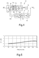
- Figure 4 shows a digital phase-locked loop 10 designed to receive an input signal s i (t), and comprising:
- the digital phase-locked loop 10 receives at input samples of the input signal s i (t), sampled with a sampling frequency F c ; consequently, the digital phase-locked loop 10 operates in the discrete-time domain.
- F c sampling frequency
- the digital phase-locked loop 10 does not have a single reference signal s vco (t) on the feedback branch, but rather two quadrature tones, i.e., two sinusoidal signals having, but for a fixed phase offset of 90 degrees, the same phase, equal to the aforementioned reference phase ⁇ VCO (t), equal to ⁇ VC ⁇ O t + K VCO ⁇ V o t ⁇ dt .
- ⁇ i and ⁇ VCO represent the Laplace transforms of the phase ⁇ i (t) of the input signal s i (t) and of the reference phase ⁇ VCO (t)
- ⁇ G is the group delay introduced by the FIR filters 22a and 22b of the phase detector 20.
- the delay ⁇ G is equal to N/(2F c ).
- the phase detector 20 described has a quasi-ideal behaviour since it supplies the difference between the phase ⁇ i (t) of the input signal s i (t) and the reference phase ⁇ VCO (t), introducing only a delay due to the presence of the FIR filters 22a and 22b.
- H( ⁇ ) is the transfer function of the digital phase-locked loop 10 with respect to the modulating signal X(t).
- the output signal V o (t) corresponds to the modulating signal X(t) but for variations of amplitude and of phase that depend upon the transfer function H( ⁇ ).
- the transfer function H( ⁇ ) is such that, in the presence of a non-sinusoidal input signal s i (t), it undergoes a contained linear distortion such that the digital phase-locked loop 10 described is particularly effective when used as demodulator of frequency-modulated signals.
- the performance of the digital phase-locked loop 10 can be appreciated also from an analysis of the plot of the signal-to-noise ratio SNR OUT of the output signal V o (t) with respect to the signal-to-noise ratio SNR IN of the input signal s i (t), and in particular from an analysis of the signal-to-noise ratio SNR OUT where there occurs the threshold phenomenon, characteristic of phase-locked loops.
- said threshold phenomenon consists in the presence of a value of signal-to-noise ratio SNR OUT equal to the signal-to-noise ratio SNR IN of the input signal s i (t) less 1 dB, a value beyond which the values of the signal-to-noise ratio SNR OUT of the output signal V o (t) become greater than the corresponding values of the signal-to-noise ratio SNR IN of the input signal s i (t).
- the present digital phase-locked loop 10 has threshold values at values of the signal-to-noise ratio SNR OUT of the output signal V o (t) of approximately 4 dB, i.e., threshold values at least 2 dB lower than the threshold values characteristic of the main demodulators for frequency-modulated signals available on the market, such as for example frequency discriminators.
- the presence of a unitary filter 3a guarantees the stability of the digital phase-locked loop 10 with a sufficient stability margin, which can be calculated, once the sampling frequency F c of the input signal s i (t) is known, by means of the equation K VCO ⁇ ( ⁇ lN ) *F C , obtained by applying the known stability criteria for feedback systems, as described in greater detail in what follows.
- the digital phase-locked loop 10 can be implemented, by using a corresponding software module, either by a microprocessor, such as for example a DSP (Digital Signal Processor), or by an FPGA (Field Programmable Gate Array).
- a microprocessor such as for example a DSP (Digital Signal Processor), or by an FPGA (Field Programmable Gate Array).
- an advantageous embodiment of the digital phase-locked loop 10 envisages that both the sine and cosine functions of the QVCO 40 and the arctangent function of the calculation block 23 are calculated by means of approximations linked to polynomial developments (developments in Taylor series) of the respective arguments.
- the calculation block 23 verifies the sign of the quadrature component s iq (t) (step 52): if the amplitude Q of the quadrature component s iq (t) is positive, the calculation block 23 sets y equal to n/2 (step 54); if it is negative, the calculation block 23 sets y equal to - ⁇ /2 (step 56); if it is zero, the calculation block 23 sets y equal to 0 (step 58).
- the calculation block 23 computes the argument z , equal to the ratio between the amplitude Q of the quadrature component s iq (t) and the amplitude I of the in-phase component s ii (t) (step 60), and verifies the sign thereof (step 62).
- the calculation block 23 sets the argument z equal to its absolute value abs(z) (step 64) since for the subsequent steps only the modulus of the argument z is relevant.
- the calculation block 23 calculates a support variable V, after prior verification of the modulus of the argument z (step 66).
- the support variable V is calculated in the following way:
- the calculation block 23 determines to which quadrant the angle to be calculated belongs (block 74):
- the calculation described enables calculation of the arctangent function through 360° without resorting to the use of lookup tables, with the advantage of saving data memory and being able to calculate the arctangent function for exact values of the argument and not for values interpolated starting from values present in the lookup table.
- the present digital phase-locked loop 10 is suited to multiple uses, and in particular can be advantageously integrated in a receiver of frequency-modulated signals in the VHF/UHF (Very High Frequency/Ultra High Frequency) band.
- VHF/UHF Very High Frequency/Ultra High Frequency
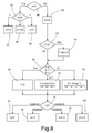
- Figure 9 shows a digital-processing system 30, i.e., the part of receiver that is typically set downstream of a corresponding analog receiving unit (receiving antenna, filters, etc.), not illustrated in Figure 9 .
- a digital-processing system 30 i.e., the part of receiver that is typically set downstream of a corresponding analog receiving unit (receiving antenna, filters, etc.), not illustrated in Figure 9 .
- the digital-processing system 30 comprises:
- the digital-processing system 30 and the digital phase-locked loop 10 comprised therein can be designed in the way that is described hereinafter, which regards a non-limiting illustrative situation, in which the input signal s i (t) has a frequency F 0 , hereinafter for reasons of convenience defined as "carrier frequency”, and is frequency-modulated with a modulating signal X(t) having a modulating frequency F m comprised in the audio band 300-3300 Hz, i.e., having a maximum frequency F max of 3300 Hz; the maximum frequency deviation ⁇ F of the modulated signal is 6500 Hz.
- an intermediate frequency F IF of the analog receiving unit is assumed as being 437.5 kHz
- a translation frequency F ol of the harmonic translation signal is assumed as being 112.5 kHz.
- the carrier frequency F 0 is 25 kHz, given the aforementioned values of the intermediate frequency F IF of the receiving unit (437.5 kHz) and of the translation frequency F ol of the harmonic translation signal (112.5 kHz), in addition to the selection, not described in detail in so far as it is based upon known signal-processing techniques, of the replica of the signal s fe (t) processed by the analog receiving unit that is closest to the baseband.
- the signal V o (t) at output from the digital phase-locked loop 10 has a residual modulation index ⁇ R equal to the amplitude of the error signal ⁇ (t) produced by the phase detector 20.
- the aforementioned value of residual modulation index ⁇ R must be lower than ⁇ , to guarantee hold of the phase locking.
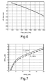
- the residual modulation index ⁇ R determines the mask that must be implemented by the FIR filters 22a and 22b, an illustrative example of which is given in Figure 10 .
- the FIR filters 22a and 22b must have a passband (cutoff frequency) equal to at least ( ⁇ R +1)F max , with ⁇ R generally set at ⁇ , with the consequence that the carrier frequency F 0 of the input signal s i (t) must be higher than ( ⁇ R +1)F max .
- the carrier frequency F 0 of the input signal s i (t) must be less than, or at the most equal to, one fourth of the sampling frequency F c ; i.e., it must be F 0 ⁇ F C 4 so that the frequency 2F 0 , i.e., twice the carrier frequency F 0 of the input signal s i (t), is equal to or less than the Nyquist frequency, equal to F c /2, i.e., half the sampling frequency.
- the stop-band frequency of the FIR filters 22a and 22b can be set equal to 2F 0 -( ⁇ R +1)F max .
- the attenuation introduced by the FIR filters 22a and 22b can be chosen so that the number N of coefficients of the FIR filters 22a and 22b is minimum, at the same time observing the constraints imposed to satisfy the stability criteria, summarized in the following equation: F c 2 ⁇ N > F max In particular, Eq.
- (11) expresses mathematically the constraint that the frequency at which the open-loop transfer function of the digital phase-locked loop 10 introduces a phase offset of 90 degrees is higher than the maximum frequency F max of the modulating signal X(t), i.e., that the frequency of oscillation of the loop falls outside the audio band.
- Eq. (13) derives, instead, from application of the known stability criteria for feedback systems to the digital phase-locked loop 10 described.
- H loop K VCO j ⁇ ⁇ ⁇ e - j ⁇ ⁇ G the condition
- H loop ( ⁇ g ⁇ /2)
- the digital phase-locked loop 10 can be effectively used in the demodulation of input signals s i (t) that are frequency-modulated and affected by the Doppler effect, for example because they are emitted by a source moving at a speed v.
- the present digital phase-locked loop 10 proves to be only slightly influenced by the Doppler effect, which causes a frequency shift of the spectrum of the input signal s i (t) equal to the ratio between the speed v of the source and the wavelength X of the input signal s i (t), obtained as ratio between the speed of light in a vacuum and the carrier frequency F 0 .
- the field of application of the present digital phase-locked loop is not limited to the field of demodulation of frequency-modulated input signals, but rather can be extended to other applications, such as, for example, reconstruction of subcarriers in the presence of digitally modulated signals.
Landscapes
- Stabilization Of Oscillater, Synchronisation, Frequency Synthesizers (AREA)
- Digital Transmission Methods That Use Modulated Carrier Waves (AREA)
Applications Claiming Priority (1)
| Application Number | Priority Date | Filing Date | Title |
|---|---|---|---|
| ITTO20080368 ITTO20080368A1 (it) | 2008-05-15 | 2008-05-15 | Anello digitale ad aggancio di fase |
Publications (2)
| Publication Number | Publication Date |
|---|---|
| EP2120342A1 true EP2120342A1 (de) | 2009-11-18 |
| EP2120342A8 EP2120342A8 (de) | 2010-05-19 |
Family
ID=40303097
Family Applications (1)
| Application Number | Title | Priority Date | Filing Date |
|---|---|---|---|
| EP09160318A Withdrawn EP2120342A1 (de) | 2008-05-15 | 2009-05-14 | Digitaler Phasenregelkreis |
Country Status (2)
| Country | Link |
|---|---|
| EP (1) | EP2120342A1 (de) |
| IT (1) | ITTO20080368A1 (de) |
Cited By (1)
| Publication number | Priority date | Publication date | Assignee | Title |
|---|---|---|---|---|
| CN112671398A (zh) * | 2020-12-08 | 2021-04-16 | 东北大学 | 一种非正弦周期信号锁相方法及系统 |
Citations (3)
| Publication number | Priority date | Publication date | Assignee | Title |
|---|---|---|---|---|
| US5742207A (en) * | 1996-07-25 | 1998-04-21 | Rockwell International Corporation | Tracking loop having instantaneous frequency shift protection |
| WO2002091578A2 (en) * | 2001-05-09 | 2002-11-14 | Masoud Karimi Ghartemani | Phase-locked loop system |
| US20030219082A1 (en) * | 2002-02-28 | 2003-11-27 | Katsuyuki Tanaka | Demodulation apparatus and receiving apparatus |
-
2008
- 2008-05-15 IT ITTO20080368 patent/ITTO20080368A1/it unknown
-
2009
- 2009-05-14 EP EP09160318A patent/EP2120342A1/de not_active Withdrawn
Patent Citations (3)
| Publication number | Priority date | Publication date | Assignee | Title |
|---|---|---|---|---|
| US5742207A (en) * | 1996-07-25 | 1998-04-21 | Rockwell International Corporation | Tracking loop having instantaneous frequency shift protection |
| WO2002091578A2 (en) * | 2001-05-09 | 2002-11-14 | Masoud Karimi Ghartemani | Phase-locked loop system |
| US20030219082A1 (en) * | 2002-02-28 | 2003-11-27 | Katsuyuki Tanaka | Demodulation apparatus and receiving apparatus |
Cited By (1)
| Publication number | Priority date | Publication date | Assignee | Title |
|---|---|---|---|---|
| CN112671398A (zh) * | 2020-12-08 | 2021-04-16 | 东北大学 | 一种非正弦周期信号锁相方法及系统 |
Also Published As
| Publication number | Publication date |
|---|---|
| EP2120342A8 (de) | 2010-05-19 |
| ITTO20080368A1 (it) | 2009-11-16 |
Similar Documents
| Publication | Publication Date | Title |
|---|---|---|
| RU2115222C1 (ru) | Устройство для компенсации фазового сдвига в цепи обратной связи усилителя мощности (варианты) | |
| KR101140333B1 (ko) | 직교 검출기 및 그것을 이용한 직교 복조기 및 샘플링직교 복조기 | |
| JP3017041B2 (ja) | 自動周波数制御方法及びその装置 | |
| US20050096000A1 (en) | Zero if complex quadrature frequency discriminator & FM demodulator | |
| US20060057996A1 (en) | High frequency low noise phase-frequency detector and phase noise reduction method and apparatus | |
| US4862098A (en) | Continuous-wave-modulation detectors using prediction methods | |
| Geng et al. | Advanced topics on RF amplitude and phase detection for low-level RF systems | |
| WO2011086640A1 (ja) | 送信装置、無線通信装置及び送信方法 | |
| EP2120342A1 (de) | Digitaler Phasenregelkreis | |
| Naeem et al. | Doppler shift compensation techniques for LEO satellite on-board receivers | |
| US7511469B2 (en) | Phase measurement device using inphase and quadrature components for phase estimation | |
| JP2994836B2 (ja) | 復調器のafc回路 | |
| AU650170B2 (en) | Phase divider for complex signals | |
| WO2000064051A1 (en) | Carrier tracking method | |
| JP3717856B2 (ja) | 周波数測定装置 | |
| US6914945B2 (en) | Clock recovery circuit | |
| Xue et al. | A new method of an IF I/Q demodulator for narrowband signals | |
| JP2765601B2 (ja) | 復調回路 | |
| WO2005006694A1 (ja) | タイミング抽出装置及び方法並びにそのタイミング抽出装置を備えた復調装置 | |
| EP1217724A1 (de) | Quadratur-Demodulator | |
| JP2837914B2 (ja) | Afc装置 | |
| JPH06237277A (ja) | Psk搬送波信号再生装置 | |
| EP2797225B1 (de) | Verfahren und Vorrichtung zur Demodulation eines amplitudenmodulierten Signals | |
| JP3462277B2 (ja) | 搬送波再生回路 | |
| KR0132963B1 (ko) | 반송파 복구장치 |
Legal Events
| Date | Code | Title | Description |
|---|---|---|---|
| PUAI | Public reference made under article 153(3) epc to a published international application that has entered the european phase |
Free format text: ORIGINAL CODE: 0009012 |
|
| AK | Designated contracting states |
Kind code of ref document: A1 Designated state(s): AT BE BG CH CY CZ DE DK EE ES FI FR GB GR HR HU IE IS IT LI LT LU LV MC MK MT NL NO PL PT RO SE SI SK TR |
|
| 17P | Request for examination filed |
Effective date: 20091216 |
|
| GRAP | Despatch of communication of intention to grant a patent |
Free format text: ORIGINAL CODE: EPIDOSNIGR1 |
|
| STAA | Information on the status of an ep patent application or granted ep patent |
Free format text: STATUS: THE APPLICATION IS DEEMED TO BE WITHDRAWN |
|
| 18D | Application deemed to be withdrawn |
Effective date: 20110426 |